Identification of a strong contamination source for graphene in vacuum systems
Abstract
To minimize parasitic doping effects caused by uncontrolled material adsorption, graphene is often investigated under vacuum. Here we report an entirely unexpected phenomenon occurring in vacuum systems, namely strong n-doping of graphene due to chemical species generated by common ion high-vacuum gauges. The effect – reversible upon exposing graphene to air – is significant, as doping rates can largely exceed cm-2/hour, depending on pressure and the relative position of the gauge and the graphene device. It is important to be aware of the phenomenon, as its basic manifestation can be mistakenly interpreted as vacuum-induced desorption of p-dopants.
1 Introduction
The unique structural and electronic properties of graphene [1, 2] have great potential for the development of opto-electronic applications [3, 4, 5]. For instance, the superior mechanical strength and electrical conductivity of graphene are ideally suited for flexible electronic devices, such as foldable tablets. Also, the gapless graphene band structure and the high tunability of the Fermi level by gating can be exploited to realize innovative, switchable photonic devices with a wide spectral range (from THz to visible). The recent success in producing large area graphene – for instance by epitaxial growth on SiC substrate [6] or by chemical vapor deposition (CVD) [7, 8, 9, 10, 11, 12, 13] – brings all these applications significantly closer to reality.
Further technological progress will require significant improvements, both at the fundamental level and in very practical aspects of the production and characterization of graphene, to control the material, its uniformity over large areas, and its stability over time [4, 5]. Indeed, all these aspects are critical because the true two-dimensionality of graphene strongly amplifies interactions with the environment, be it the supporting substrate, or unintentionally present adsorbates. While it seems clear that an appropriate encapsulation strategy will have to be developed for future applications, most investigations of graphene are currently performed under high-vacuum conditions specifically to minimize this type of effects. In this case, desorption of adsorbates from the graphene device is the only process expected to occur. The frequent observation that graphene exposed to air is strongly p-doped, whereas after insertion in a vacuum system the doping level is significantly reduced, is often taken as evidence for exactly such vacuum-induced desorption of adsorbates.
In this paper we report an unexpected phenomenon that strongly influences the properties of graphene even under high vacuum conditions, causing pronounced time instabilities, and that is difficult to identify as it can be mistakenly attributed to desorption of adsorbates originally present on the material. Specifically, we find that even in high-vacuum systems, filaments of common ion pressure gauges produce and emit active chemical species that are adsorbed onto graphene, and that cause very large shifts in the gate voltage at which the graphene charge neutrality point occurs. We have observed the effect to be present – and to manifest itself very similarly – on graphene obtained by both CVD [7, 8, 9, 10, 11, 12, 13] and mechanical exfoliation [14], with changes in density of charge carriers much larger than cm-2/hour. This gauge-induced doping can overcome the original p-doping of the material as measured in air (even when the initial doping level is very large), eventually making the material n-doped. It can be completely reversed upon (re)exposure of graphene to air, with no apparent damage to the graphene or deterioration of its properties.
The phenomenon appears as long as the chemical species generated by the ion gauge can reach the sample before being pumped away (and therefore it sensitively depends on the position of the ion gauge in the vacuum system relative to the graphene sample). Since vacuum systems containing ion gauges are widely used by many research groups working on the characterization and production of graphene, it is important to be aware of the existence of this phenomenon, to avoid misinterpreting results of experiments performed under vacuum conditions. Recognizing this effect is equally important for the further technological development of graphene synthesis and device fabrication techniques, leading to large scale production of graphene materials with controllable and reproducible properties.
2 Sample preparation and measurement
Most of the graphene samples investigated here were grown by low-pressure CVD [7, 8, 9, 10] on a 25 m thick 99.999 % copper foil, following a two-step process derived from Ref. [8]. The Cu foil is first annealed at 1000 ∘C under a 5 sccm H2 flow at 50 mTorr for 20 minutes. Graphene is then grown in 5 sccm H2 and 7 sccm CH4 at 1035 ∘C, with an initial 4 minute growth step at 120 mTorr, and a second step increasing the growth pressure to 1 Torr over 15 seconds. Finally, the pressure is decreased back to 120 mTorr, and the samples cooled under process gas flow for 30 minutes. These parameters have been optimized to produce homogeneous graphene monolayers, with only few multilayer islands or contaminating nano-particles [15].
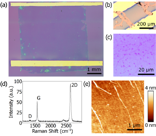
Using a PMMA-mediated technique derived from Liang et al. [16], the graphene layers were transferred onto doped silicon substrates covered by 300 nm oxide. Under high magnification optical microscopy (Fig. 1(c)), the samples appear uniform, with wrinkles and small multilayer islands distinguishable, respectively, as dark lines and spots distributed all over the sample surface. Characterization of the sample topography by atomic force microscopy (Fig. 1(e)) shows low 1 nm surface roughness, with small wrinkles and nanoparticles from the transfer process. The monolayer character of the samples is confirmed through Raman spectroscopy measurements, shown in Fig. 1(d). A high intensity ratio between the 2D (2700 cm-1) and G (1580 cm-1) bands is found, as well as a single Lorentzian profile of the 2D peak, with a width at half maximum of 34 cm-1 [17, 11]. The small intensity of the D band (1350 cm-1) demonstrates that the CVD graphene is not disordered at small length scales [18].
Two-terminal graphene devices were fabricated by the deposition of source and drain electrodes (10 nm Ti / 50 nm Au) through a shadow mask, allowing either the full samples with dimensions of about 55 mm2, or smaller 200200 m2 areas, to be measured rapidly, without the need of any lithographic processing (Figs. 1(a) and 1(b); the doped Si substrate was used as gate contact). The samples were characterized in a Lakeshore CPX probe station under vacuum, with a cold cathode ion gauge mounted directly on the chamber. The resistance was obtained by current-biasing (100 nA at 20 Hz) the graphene devices, and measuring the source-drain voltage with an SR830 lock-in amplifier. Over the large areas of our devices, the as-grown material reproducibly shows a field effect mobility of approximately 1000 cm2V-1s-1 at room temperature, increasing (also reproducibly) to approximately 1400 cm2V-1s-1 after current annealing in vacuum. For comparison, we also investigated an exfoliated graphene sample with a dimension of approximately 1010 m2 (with 1800 cm2V-1s-1, which was selected to have a mobility value close to that of CVD-grown graphene).
3 Results and discussion
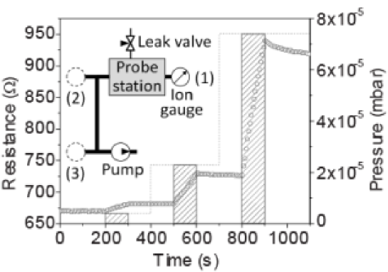
In order to distinguish between the effects of the ion gauge and of vacuum itself, the chamber was first pumped with the ion gauge kept switched off all the time, and the samples characterized at the base pressure of 1.310-6 mbar. The pressure was then stabilized at different levels up to 310-4 mbar, by using a leak valve between the chamber and the ambient environment to gradually increase the pressure in the system. For each pressure level, the ion gauge was turned on for one to a few hundred seconds to see its effect on the sample. As shown in Fig. 2, we observe an increase of the sample resistance with time whenever the ion gauge is switched on (shaded regions), and an approximately constant resistance when the gauge is switched off. Interestingly, the rate at which the device resistance varies upon switching on the ion gauge appears to increase with increasing pressure inside the chamber.
To understand the origin of the observed time dependence of the resistance, and to determine how the rate of change depends on pressure, we measured the conductivity of our devices as a function of gate voltage, after having kept the devices in vacuum with the gauge turned on for different periods of time (Fig. 3). With increasing duration of the exposure to the ion gauge, we observe a systematic shift of the conductivity curve towards more negative gate voltages. Except for the slight broadening of the width of the conductivity dip at the charge neutrality point, the shape of the curve virtually does not change. The charge carrier mobility is thus not affected by the ion gauge effect. One may be superficially led to conclude that the shift originates from vacuum-induced desorption of adsorbates attached to the graphene sheet. However, this is clearly not the case because (i) a fast shift is only observed when the gauge is turned on (when the gauge is turned off a shift is still visible, but it is normally orders of magnitude slower and smaller), and, (ii) as we discuss in detail below, the effect is slower for better vacuum in the system. All these observations can only be explained if the vacuum gauge generates chemical species that propagate through the vacuum system and that act as n-dopants once they are absorbed onto the graphene sheet.
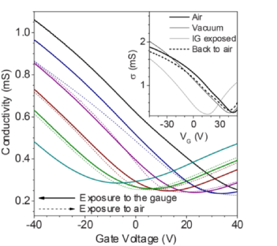
As shown by the dashed lines in Fig. 3, the effect is reversible after exposure to air, both in CVD graphene, previously annealed in vacuum to improve transport characteristics (causing p-dopant desorption, and thus a slight additional shift of the charge neutrality point), and in exfoliated, non-annealed graphene. In the latter, we measured the conductivity vs gate voltage characteristics in air, then in vacuum with the ion gauge off and with the ion gauge on, and finally after six days of recovery in air, as shown in the inset of Fig. 3. We see that the vast majority of the doping effect occurs as a result of the exposure to the gauge, and that it is completely reversed after exposure to air.
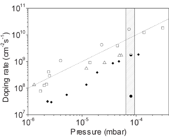
To quantify the effect of the vacuum gauge we have estimated the doping rate . The change in dopant concentration is obtained from the conductivity vs gate voltage curve (), using the known gate capacitance to convert the shift of the charge neutrality point into a shift in carrier density. As shown in Fig. 4 for several CVD-grown samples (open symbols), we find that the doping rates obtained in this way are roughly proportional to the pressure in the system, with a coefficient of proportionality of the order of 1014 cm2s-1mbar-1 (dashed line in Fig. 4). Devices made with standard exfoliated graphene (filled diamonds in Fig. 4) show qualitatively identical behavior, albeit with a slightly lower value of the coefficient . We thus conclude that the n-doping induced by the ion vacuum gauge is systematically present for all kinds of graphene devices (i.e., not only specific to our CVD grown samples).
The type of measurements just discussed can be used to provide a very direct, qualitative demonstration that the effect is indeed caused by the ion gauge. To this end, it is simply sufficient to compare the value of the parameter when repeating exactly the same experiment, but with the vacuum gauge mounted in different positions of the vacuum system as the only difference (the different positions are illustrated in the inset of Fig. 2). For a specific pressure in the vacuum system, the experimental values of thus obtained are the three data points in the shaded region of Fig. 4. The upper one (i.e. the highest ) corresponds to the case where the gauge is mounted directly on the probe station (position 1 in inset of Fig. 2). is an order of magnitude lower when the gauge is mounted in front of the chamber, on the pumping line (position 2 in inset of Fig. 2); it drops again over two orders of magnitude when the gauge is mounted close to the turbomolecular pump itself (position 3 in inset of Fig. 2). Thus, although the effect is seen irrespective of the position of the gauge in the system, its strength decreases when the gauge is mounted further away from the sample and closer to the inlet of the pump.
All our results are in line with observations reported earlier by Podzorov et al. [19] on a specific type of organic single-crystal transistors, in which the surface of the crystal where the transistor channel is formed is accessible to molecules present in the vacuum chamber. These authors also found a reversible and pressure-dependent n-doping generated from ion vacuum gauges, manifesting itself in a large shift of the device threshold voltage and – different from the case of graphene – in a strong carrier mobility suppression. Podzorov and coworkers attributed the effect to the creation of active species, possibly free radicals, on the hot gauge filament, which – when adsorbed on the organic crystal – simultaneously dope its surface (explaining the threshold voltage shift) and create localized electronic states in the gap of the organic semiconductor (accounting for the suppressed mobility).
Such an explanation fully accounts for our observation on graphene as well. Indeed, in vacuum systems, many different radicals are known to be generated by hot filaments depending on the gas species present [20, 21, 22, 23]. In our case, with the molecules reaching the hot filament of the ion gauge coming from the background pressure of our vacuum system, we certainly expect to have radicals of O, OH, H, and of different hydrocarbons (we cannot, however, determine if a specific radical plays a dominant role in the observed doping of graphene, and what the microscopic mechanism is). According to this explanation, the increase in doping rate with increasing pressure can then be the consequence of two different mechanisms. First, as the pressure is increased, the number of molecules reaching the hot filament of the ion gauge is larger, and so is the number of radicals that eventually reach the graphene layer. Such an explanation very simply accounts for the linear dependence between doping rate and pressure that is seen experimentally. Additionally, at higher pressure, the mean free path inside the vacuum system is shorter, which eventually makes the motion of the emitted radical diffusive (rather than ballistic). Diffusive motion should also result in an increase of the doping rate, because the emitted radicals have a larger probability to reach the graphene layer rather than to be adsorbed on the walls of the vacuum system. However, we expect that such a crossover in transport regime (from ballistic to diffusive) becomes relevant only at pressure of the order of 10-3 mbar or higher (out of the range that we have investigated in detail), since at lower pressure the molecular motion on the dimension of the vacuum systems used in our studies is virtually always ballistic. Finally, contrary to the case of organic semiconductors studied by Podzorov et al. [19], graphene has no band-gap, and the only visible effect of the chemical species generated from the ion gauge is to shift the charge neutrality point, without significant effects on the the carrier mobility (the mobility is likely limited by other sources of disorder in our CVD graphene layers).
In summary, it is obviously important to be fully aware of the effect of ion vacuum gauges on graphene, since the majority of research groups working on this material performs experiment or measurements in vacuum systems where these ion vacuum gauges are very commonly employed, and kept turned on all the time. The gauge-induced n-doping can be very misleading when it comes to sample characterization. Graphene samples are usually p-doped if no annealing is done prior to the measurement, and the shift of the charge neutrality point toward smaller gate voltages could be interpreted as p-dopant desorption in vacuum, whereas it is actually the result of more dopants of the opposite sign produced by the ion gauge filament, being adsorbed onto the sample surface. Clearly, having p-dopants desorbed or compensated by n-dopants would lead to a very different situations if, for instance, local sample homogeneity is a relevant issue in the experiments. Furthermore, the vacuum gauge induced doping effect occurs most intensely at high pressure, when the system is pumping prior to device measurement. Once base pressure is reached, the doping rate can become small enough to be unnoticeable over a short experimental time. It may therefore not be obvious that the ion gauge is the actual reason why n-doping is found in some samples.
4 Summary
Our observations clearly show that even in vacuum systems, where graphene is expected to be isolated from the effect of molecules present in the environment, adsorption of active chemicals generated by ion pressure gauges has a significant influence on the electronic properties of the material. Specifically, changes in carrier density occurring at a rate of up to 1013 cm-2/hour at 10-4 mbar are observed, allowing doping graphene up to a level of cm-2. The effect is difficult to identify (as it is easily mistakenly interpreted as vacuum-induced desorption of adsorbates) and appears very similarly in all kinds of graphene, both CVD-grown and exfoliated, annealed and non-annealed, as long as the chemical species generated by the vacuum gauges can reach the sample before being pumped out. As the doping effect takes place in any vacuum system in which an ion gauge is used, it is important to be aware of its existence when performing investigation or characterization of the electronic properties of graphene. Clearly, it will also be important to eliminate (or properly take into account) these effects when developing a process for the production and structuring of large-area graphene with reproducible properties, which is a key aspect in developing a robust graphene-based technology. Indeed, many key technological steps, such as annealing of graphene, contact depositions, or material etching are normally performed in vacuum systems, in which chemicals generated by vacuum ion gauges can affect the properties of graphene.
5 acknowledgements
The authors thank S. Muller and A. Ferreira for technical support, and J. Teyssier for his support on Raman spectroscopy. This work was funded by the Swiss National Science Foundation through the NCCR MaNEP and Division II grant 200020-138198.
6 References
References
- [1] Geim A K and Novoselov K S 2007 Nat. Mater. 6 183–191
- [2] Castro Neto A H, Guinea F, Peres N M R, Novoselov K S and Geim A K 2009 Rev. Mod. Phys. 81 109–162
- [3] Geim A K 2009 Science 324 1530–1534
- [4] Choi W, Lahiri I, Seelaboyina R and Kang Y S 2010 Crit. Rev. Solid State 35 52–71
- [5] Novoselov K S, Fal’ko V I, Colombo L, Gellert P R, Schwab M G and Kim K 2012 Nature 490 192–200
- [6] Berger C, Song Z, Li T, Li X, Ogbazghi A Y, Feng R, Dai Z, Marchenkov A N, Conrad E H, First P N and de Heer W A 2004 The Journal of Physical Chemistry B 108 19912–19916
- [7] Li X, Cai W, An J, Kim S, Nah J, Yang D, Piner R, Velamakanni A, Jung I, Tutuc E, Banerjee S K, Colombo L and Ruoff R S 2009 Science 324 1312–1314
- [8] Li X, Magnuson C W, Venugopal A, An J, Suk J W, Han B, Borysiak M, Cai W, Velamakanni A, Zhu Y, Fu L, Vogel E M, Voelkl E, Colombo L and Ruoff R S 2010 Nano Lett. 10 4328–4334
- [9] Levendorf M P, Ruiz-Vargas C S, Garg S and Park J 2009 Nano Lett. 9 4479–4483
- [10] Bae S, Kim H, Lee Y, Xu X, Park J S, Zheng Y, Balakrishnan J, Lei T, Ri Kim H, Song Y I, Kim Y J, Kim K S, Ozyilmaz B, Ahn J H, Hong B H and Iijima S 2010 Nat. Nanotechnol. 5 574–578
- [11] Reina A, Jia X, Ho J, Nezich D, Son H, Bulovic V, Dresselhaus M S and Kong J 2009 Nano Lett. 9 30–35
- [12] Reina A, Thiele S, Jia X, Bhaviripudi S, Dresselhaus M, Schaefer J and Kong J 2009 Nano Res. 2(6) 509–516
- [13] Kim K S, Zhao Y, Jang H, Lee S Y, Kim J M, Kim K S, Ahn J , Kim P, Choi J and Hong B H 2009 Nature 457 706–710
- [14] Novoselov K S, Geim A K, Morozov S V, Jiang D, Zhang Y, Dubonos S V, Grigorieva I V and Firsov A A 2004 Science 306 666–669
- [15] Small particles can be formed during graphene growth, as previously reported in Ref. [16]. Using scanning electron microscopy, we have additionally observed that growth conditions can modify the nanoparticle density, size (from 100 nm to 1 m), and shape (from rounded to tetragonal). We suggest that, because of their tetragonal shape, the observed nanoparticles are nanodiamonds, although the presence of Cu residues cannot be completely excluded.
- [16] Liang X, Sperling B A, Calizo I, Cheng G, Hacker C A, Zhang Q, Obeng Y, Yan K, Peng H, Li Q, Zhu X, Yuan H, Hight Walker A R, Liu Z, Peng L m and Richter C A 2011 ACS Nano 5 9144–9153; Here we used HCl 30 % with a few drops of H2O2 30 % as the Cu etchant.
- [17] Ferrari A C, Meyer J C, Scardaci V, Casiraghi C, Lazzeri M, Mauri F, Piscanec S, Jiang D, Novoselov K S, Roth S and Geim A K 2006 Phys. Rev. Lett. 97 187401
- [18] Ferrari A C 2007 Solid State Commun. 143 47–57
- [19] Podzorov V, Menard E, Pereversev S, Yakshinsky B, Madey T, Rogers J A and Gershenson M E 2005 Appl. Phys. Lett. 87 093505
- [20] Smith J A, Cameron E, Ashfold M N R, Mankelevich Y A and Suetin N V 2001 Diamond and Related Materials 10 358-363
- [21] Duan H L, Zaharias G A and Bent S F 2002 Current Opinion in Solid State and Materials Science 6 471-477
- [22] Umemoto H, Ohara K, Morita D, Morimoto T, Yamawaki M, Masuda A and Matsumura H 2003 Jpn. J. Appl. Phys. 42 5315
- [23] Umemoto H and Kusanagi H 2009 The Open Chem. Phys. Journal 2 32-36