Beam Test Studies of 3D Pixel Sensors Irradiated Non-Uniformly
for the ATLAS Forward Physics Detector
Abstract
Pixel detectors with cylindrical electrodes that penetrate the silicon substrate (so called 3D detectors) offer advantages over standard planar sensors in terms of radiation hardness, since the electrode distance is decoupled from the bulk thickness. In recent years significant progress has been made in the development of 3D sensors, which culminated in the sensor production for the ATLAS Insertable B-Layer (IBL) upgrade carried out at CNM (Barcelona, Spain) and FBK (Trento, Italy). Based on this success, the ATLAS Forward Physics (AFP) experiment has selected the 3D pixel sensor technology for the tracking detector. The AFP project presents a new challenge due to the need for a reduced dead area with respect to IBL, and the in-homogeneous nature of the radiation dose distribution in the sensor. Electrical characterization of the first AFP prototypes and beam test studies of 3D pixel devices irradiated non-uniformly are presented in this paper.
keywords:
ATLAS upgrade, pixel detectors, 3D pixels, radiation hardness, high energy physics1 Introduction
ATLAS [1] intends to install a Forward Physics detector (AFP) in order to identify diffracted protons at 210 m from the interaction point [2] in 2018. The current AFP design foresees a high resolution pixelated silicon tracking system combined with a timing detector for the removal of pile up protons. The AFP tracker unit will consist of an array of six pixel sensors placed at 2-3 mm from the Large Hadron Collider (LHC) proton beam. The proximity to the beam is essential for the AFP physics program as it directly increases the sensitivity of the experiment [2]. Thus, there are two critical requirements for the AFP pixel detector: first, the active area of the detector has to be as close as possible to the LHC beam, which means that the dead region of the sensor has to be minimized. Second, the device has to be able to cope with a very inhomogeneous radiation distribution. Preliminary estimations indicate that the side of the sensors close to the beam will have to sustain a fluence equivalent to 1 MeV neutrons222The non-ionising energy loss will be quoted as the equivalent damage of a fluence of 1 MeV neutrons: neq/cm2., while the opposite site is expected to receive several orders of magnitude less radiation [3].
Based on the successful performance of CNM [4] and FBK [5] 3D sensors productions [6] for the ATLAS Insertable B-Layer (IBL) [7], the 3D technology was chosen for the AFP tracking detector. However, the IBL sensors have a large inactive edge on the side which will be closest to the beam in the AFP configuration. To meet the AFP requirements, different dicing techniques have been investigated to reduce the dead area of the IBL 3D sensors.
As silicon sensors are irradiated the space charge in the detector bulk changes, eventually leading to an increase in the full depletion voltage. Since the radiation distribution of the AFP silicon sensors will be highly non-uniform, there can be a scenario where the breakdown voltage of the non-irradiated zone is lower than the depletion voltage of the irradiated one. This will degrade the device performance: a high bias voltage will increase the leakage current leading to noise (to a point where the device may not longer be operated), while an intermediate voltage will reduce the amount of charge collected in the irradiated area, degrading the hit reconstruction efficiency. Thus sensors with high initial breakdown voltage will be ideal for AFP.
This paper introduces the AFP pixel module in Section 2. Section 3 presents the results of electrical tests performed on slim-edge prototypes. The non-uniform irradiation of 3D sensors is described in Section 4. Finally, in Section 5, the performance of the irradiated devices in beam tests is presented.
2 The AFP Pixel Module
The pixel readout electronics of AFP will be the FE-I4 [8] chip, which was developed for IBL. Built in the 130 nm CMOS process, the FE-I4 offers an increased tolerance to radiation with respect to the current ATLAS pixel readout chip, the FE-I3 [9]. The IBL chip features an array of pixels with a pixel size of m2. The total size of the FE-I4 chip is mm2 and the active fraction is 89%. The sensors are DC coupled to the chip with negative charge collection. Each readout channel contains an independent amplification stage with adjustable shaping, followed by a discriminator with independently adjustable threshold. The chip operates with a MHz externally supplied clock. The time over threshold (ToT) with -bit resolution together with the firing time are stored for a latency interval until a trigger decision is taken.
The selected sensor for AFP is the IBL 3D sensor, since it provides high radiation tolerance at low bias voltage [10]. The IBL 3D sensor is 230 m thick with the n- and p-type columns etched from the opposite sides of the p-type substrate. The pixel configuration consists of two n-type readout electrodes connected at the wafer surface along the 250 m long pixel direction, surrounded by six p-type electrodes which are shared with the neighboring pixels. The CNM 3D sensor design features m long columns which are isolated on the n+ side with p-stop implants. The edge isolation is accomplished with a combination of a n+ 3D guard ring, which is grounded, and fences, which are at the bias voltage potential from the ohmic side.
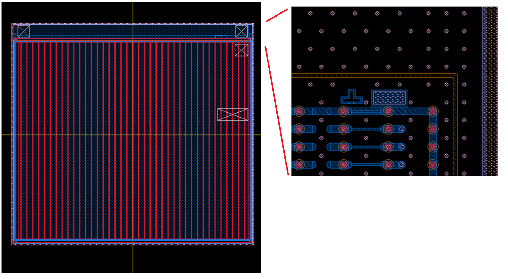
The IBL sensor design has a large (1mm) dead region in the side opposite to the wirebonds, see Fig 1. This dead region was added to accommodate the bias stab needed for the active edge technology which was finally not incorporated into the IBL (the side opposite to the wirebonds is not critical for the IBL, since the sensors overlap in the direction). However, for the AFP project, it is critical to substantially reduce the mentioned dead area, since it will be closest to the beam.
In order to adapt the 3D IBL sensors for AFP, different techniques have been investigated. Detectors were post-processed using the scribe-cleave-passivate (SCP) technology to reduce the dead area. Details of SCP method have been described in other publications [11]. The method relies on passivating the sidewall with low defect density. A low defect density is obtained in a two-step process. First, the surface of the sensor is scribed at the desired edge location in the direction that coincides with one of the silicon crystal planes. Then the peripheral region is mechanically cleaved off. The resulting sidewall follows the crystal plane. The passivation step uses dielectric material that depends on the bulk type of the silicon. For p-type wafers used in this study, a dielectric with negative interface charge on the border with silicon is needed. This is accomplished by depositing an atomic layer (ALD) of Al2O3. Standard diamond-saw cuts were also investigated [12], but are not presented here.
3 Electrical Tests of the First 3D Sensors Prototypes for AFP
The SCP technology has been used to reduce the inactive area of the IBL sensors for AFP. Since a limited number of sensors were available at the time, the technique was first tested on 3D sensors designed for the FE-I3 readout chip. The m-thick FE-I3 3D sensors feature an array of pixels. Each m2 pixel is defined by three m deep n-type readout columns, surrounded by eight p-type column electrodes. Though the pixel geometry is different, the results are expected to be relevant for the FE-I4 sensors, since the slim edge performance mostly depends on characteristics of the sensor periphery: sensor thickness, slim edge distance, and sidewall treatment.
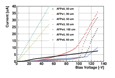
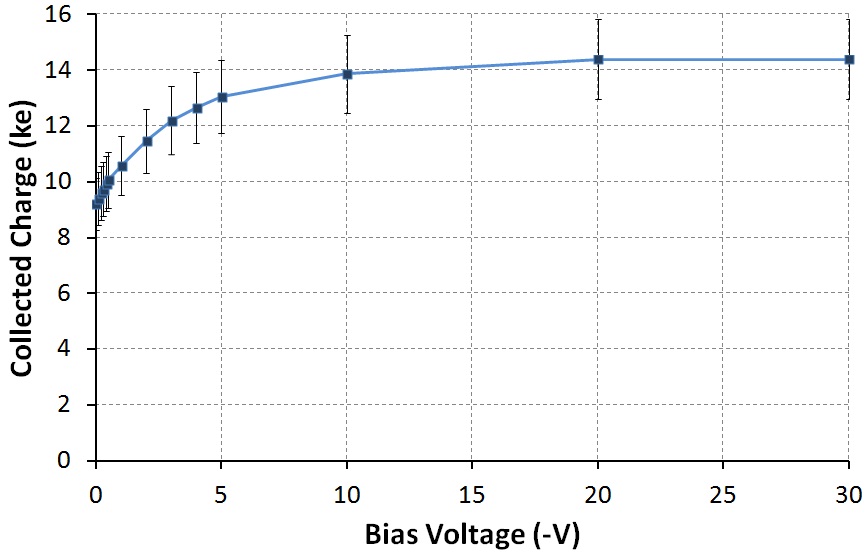
Seven CNM 3D FE-I3 devices which presented breakdown voltages above V were sent to NRL [13] to reduce the dead region by applying the SCP technology, from the original mm to m. The devices were returned to Barcelona to be bump-bonded to FE-I3 readout chips and characterized. Figure 2 shows the leakage currents as a function of the bias voltage measured at room temperature. Two assemblies show a resistive behavior. This may be caused by defects on the sidewall due to imperfect cleaving process. The charge collection was verified in devices without resistive behavior using a 90-Sr source and an external trigger provided by a scintillator. Figure 2 presents the most probable value (MPV) of the Landau fit to the charge distribution. Since the devices are 230 m thick, the expected charge at full depletion is about 15 k electrons, which is within the systematic uncertainties of the measurement above 10 V.
4 Non-uniform Irradiation of 3D Sensors
One critical aspect of the pixel devices for the AFP forward detector is the non-uniform nature of the radiation distribution across the sensor. AFP pixel devices must be able to operate with high efficiency when only a portion of the sensor is irradiated to neq/cm2. This means that the less irradiated areas of the sensor have to sustain high bias voltages keeping the leakage current at moderate values. Previous experiences with FE-I4 CNM 3D devices indicated that the leakage current has to be lower than 200 A (front-end chip not powered) in order to maintain low noise levels and ensure high hit reconstruction efficiency [10].
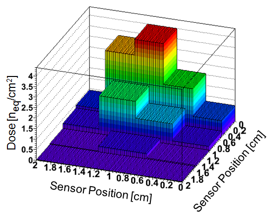
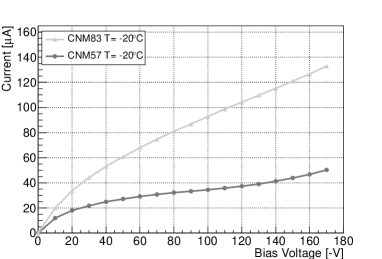
To study the effect of non-uniform irradiations, two FE-I4 IBL prototypes (CNM-57 and CNM-83, without slim edges) were irradiated with protons non-uniformly at the IRRAD1 facility at CERN-PS [14]. The irradiation levels are listed in Table 1. Figure 3 shows the irradiation dose distribution on CNM-57, a similar profile was obtained for CNM-83 but with a larger maximum dose.
The leakage currents measured as a function of the bias voltage for CNM-57 and CNM-83 are shown in Fig. 4. The measurements were taken at C with the front-end electronics not powered333The temperature was determined with a Pt-1000 temperature sensor on the module.. The device with early breakdown before irradiation shows a large leakage current at intermediate bias voltages (150 V), an indication that its performance may not be optimal due to the noise induced by the dark current.
| Sample | Max. Dose | Pre-Irradiation | Bias Voltage |
|---|---|---|---|
| ( neq/cm2) | Breakdown | during Beam | |
| Voltage (v) | Tests (V) | ||
| CNM-57 | 4.0 | 75 | 130 |
| CNM-83 | 9.4 | 10 | 130 |
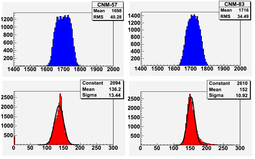
Before the performance of the devices is studied in beam tests, it is necessary to verify that the front-end electronics was not damaged as a result of the proton irradiation. The operational threshold was set to electrons based on previous experience with the IBL devices [7]. The threshold distributions of the two irradiated devices, shown in Fig. 5, present good uniformity, while the ENC (Equivalent Noise Charge) is below 200 electrons.
5 Beam Test Studies of Non-uniformly Irradiated 3D Sensors
Test beam studies of non-uniformly irradiated devices are essential to understand the AFP pixel detector module performance. Critical parameters, such as hit efficiency and position resolution, can only be determined at beam tests. Both CNM-83 and CNM-57, together with an un-irradiated reference device, have been characterized using 120 GeV pions at the CERN SPS H6 beam line in August 2012.
Beam particle trajectories were reconstructed using the high resolution EUDET telescope [16]. The telescope consists of six Mimosa tracking planes, the readout data acquisition system and the trigger hardware, and provides a m track pointing resolution. The devices under test, cooled to C, were placed between the telescope planes. Data presented here were recorded at perpendicular incident angle. The hit efficiency is determined from extrapolated tracks on the devices, after track quality cuts have been applied. A hit on the device under test is searched for in a pixel window around the track position.
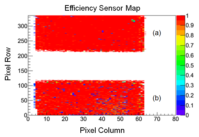
Since the active area of the FE-I4 devices is larger than the Mimosa sensors of the telescope, separate sets of data were taken to cover the irradiated and non-irradiated regions of the sensors. Fig. 6 shows the efficiency map for sensor CNM-57. The non-irradiated region has an average efficiency of , while the efficiency for the irradiated side is . If the dead and noise pixel cells (due to front-end issues) are removed, the efficiency increases to . In order to highlight the pixel structure, the corresponding efficiency as function of the track hit position folded into a two by two cell is also shown in Fig. 6. As the device is positioned perpendicular to the particle beam the effect of the pass-through electrodes is evident. The efficiency for sensor CNM-83 on the irradiated side was much lower, about , due to the large noise induced by the leakage current. This was expected from the electrical measurements done before the beam tests. In fact, it was difficult to operate the device during the beam test because the noise affected the data readout synchronization.
6 Conclusions
The AFP project presents a new challenge for pixel detectors: reduced dead areas are needed to maximize the physics potential of the experiment, and the sensors have to be able to sustain a highly non-uniform irradiation distribution. The scribe-cleave-passivate technology used to reduce the inactive edge of 3D sensors showed promising results with FE-I3 devices. The first FE-I4 prototypes have already been produced and will be tested shortly. The first beam test studies of non-uniformly irradiated 3D pixel sensors have been presented. For devices with low initial breakdown, the performance is poor due to the large leakage current caused by the bias voltage needed to deplete the irradiated area. Devices that show good electrical behavior before irradiation are able to sustain the voltage needed to achieve excellent efficiency ( at perpendicular incidence) throughout the sensor.
Acknowledgment
This work was partially funded by the MINECO, Spanish Government, under the grant FPA2010-22060-C02-01/02, and the European Commission under the FP7 Research Infrastructures project AIDA, grant agreement no. 262025. We would like to thank the Institute for Nanoscience (NSI) at the U.S. Naval Research Laboratory (NRL) and the NSI staff. The work done at NRL was sponsored by the Office of Naval Research (ONR). The work at SCIPP was supported by Department of Energy, grant DE-FG02-04ER41286.
References
- [1] The ATLAS Collaboration, “The ATLAS Experiment at the CERN Large Hadron Collider”, JINST 3 S08003 (2008).
- [2] The ATLAS Collaboration, “Letter of Intent for the Phase-I Upgrade of the ATLAS Experiment”, CERN-LHCC-2011-012, 2011.
- [3] L. Adamczyk et al., “AFP: A proposal to install proton detectors at 220 m around ATLAS to complement the ATLAS high luminosity physics program”, ATL-COM-LUM-2011-006, CERN (2011), AFP technical proposal.
- [4] Centro Nacional de Microelectronica (CNM), Barcelona (Spain), http://www.imb-cnm.csic.es/.
- [5] Fondazione Bruno Kessler (FBK), Trento (Italy), http://www.fbk.eu/.
- [6] C. Da Via et al., Nucl. Instrum. and Methods in Phys. Res. A 694 (2012) 321–330
- [7] The ATLAS IBL Collaboration, “Prototype ATLAS IBL Modules using the FE-I4A Front-End Readout Chip”, submitted to JINST, http://arxiv.org/abs/1209.1906.
- [8] M. Garcia-Sciveres et al., Nucl. Instrum. Methods Phys. Res. A 636, S155 (2011).
- [9] I. Peric, et al., Nucl. Instrum. Methods in Phys. Res. A 565, 178 (2006).
- [10] S. Grinstein, The ATLAS Collaboration, Nucl. Instrum. Methods in Phys. Res. A 699, 61 (2013).
- [11] M. Christophersen, V. Fadeyev, B.F. Phlips, H. F.-W. Sadrozinski, C. Parker, S. Eli, J.G. Wright, Nucl. Instrum. Meth. in Phys. Res. A 699 (2013) 14.
- [12] M. Povoli et al., “Slim edges in double-sided silicon 3D detectors”, July 2011, presented at iWoRID 2011, Zurich.
- [13] U.S. Naval Research Laboratory, Washington, USA.
- [14] M. Glaser, M. Huhtinen, F. Lemeilleur, C. Leroy, P. Roy, M. Tavlet, “Radiation Test Facilities in the New PS East Hall at CERN”, in Proc.5th Eur. Conf. Radiation and Its Effects Components and Systems, Fontevraud, France, 2000, pp. 136-141.
- [15] M. Glaser, F. Ravotti, M. Moll, “Dosimetry Assessments in the Irradiation Facilities at the CERN-PS Accelerator”, IEEE Trans. Nucl. Sci, vol. 53 (4), pp. 2016-2022, 2006.
- [16] E. Corrin, Nuclear Science Symposium Conference Record (NSS/MIC), 2009 IEEE, 816 (2009).