EUROPEAN ORGANIZATION FOR NUCLEAR RESEARCH (CERN)
![[Uncaptioned image]](/html/1302.5259/assets/x1.png) CERN-LHCb-DP-2012-005
21 February 2013
CERN-LHCb-DP-2012-005
21 February 2013
Radiation damage in the LHCb Vertex Locator
The LHCb VELO group111Authors are listed on the following pages.
The LHCb Vertex Locator (VELO) is a silicon strip detector designed to reconstruct charged particle trajectories and vertices produced at the LHCb interaction region. During the first two years of data collection, the VELO sensors have been exposed to a range of fluences up to a maximum value of approximately neutron equivalent (). At the operational sensor temperature of approximately , the average rate of sensor current increase is per , in excellent agreement with predictions. The silicon effective bandgap has been determined using current versus temperature scan data after irradiation, with an average value of obtained. The first observation of sensor type inversion at the LHC has been made, occurring at a fluence of around of . The only sensors in use at the LHC have also been studied. With an initial fluence of approximately , a decrease in the Effective Depletion Voltage (EDV) of around V is observed, attributed to oxygen induced removal of boron interstitial sites. Following this initial decrease, the EDV increases at a comparable rate to the type inverted type sensors, with rates of and measured for and type sensors, respectively. A reduction in the charge collection efficiency due to an unexpected effect involving the second metal layer readout lines is observed.
LHCb VELO group
A. Affolder1, K. Akiba2 M. Alexander3, S. Ali4, M. Artuso5, J. Benton6, M. van Beuzekom4, P.M. Bjørnstad7, G. Bogdanova8, S. Borghi3,7, T.J.V. Bowcock1, H. Brown1, J. Buytaert9, G. Casse1, P. Collins9, S. De Capua7, D. Dossett10, L. Eklund3, C. Farinelli4, J. Garofoli5, M. Gersabeck9, T. Gershon9,10, H. Gordon11, J. Harrison7, V. Heijne4, K. Hennessy1, D. Hutchcroft1, E. Jans4, M. John11, T. Ketel4, G. Lafferty7, T. Latham10, A. Leflat8,9, M. Liles1, D. Moran7, I. Mous4, A. Oblakowska-Mucha12, C. Parkes7, G.D. Patel1, S. Redford11, M.M. Reid10, K. Rinnert1, E. Rodrigues3,7, M. Schiller4, T. Szumlak12, C. Thomas11, J. Velthuis6, V. Volkov8, A.D. Webber7, M. Whitehead10, E. Zverev8.
1Oliver Lodge Laboratory, University of Liverpool, Liverpool, United Kingdom
2Universidade Federal do Rio de Janeiro (UFRJ), Rio de Janeiro,
Brasil
3School of Physics and Astronomy, University of Glasgow, Glasgow, United Kingdom
4Nikhef National Institute for Subatomic Physics, Amsterdam, Netherlands
5Syracuse University, Syracuse, NY, United States
6H.H. Wills Physics Laboratory, University of Bristol, Bristol, United Kingdom
7School of Physics and Astronomy, University of Manchester, Manchester, United Kingdom
8Institute of Nuclear Physics, Moscow State University (SINP MSU), Moscow, Russia
9European Organization for Nuclear Research (CERN), Geneva, Switzerland
10Department of Physics, University of Warwick, Coventry, United Kingdom
11Department of Physics, University of Oxford, Oxford, United Kingdom
12AGH University of Science and Technology, Krakow, Poland
1 Introduction
The VErtex LOcator (VELO) is a silicon strip detector positioned around the proton-proton interaction region at the LHCb [1] experiment. To obtain the precision vertexing required for heavy-flavour physics, the closest active silicon sensor region is located from the beam axis, while the silicon edge is located at a distance of mm. For the luminosity delivered by the LHC in and , the VELO was exposed to higher particle fluences than any other silicon detector at the LHC. Careful monitoring of radiation damage to the sensors is essential to ensure the quality of data for LHCb physics analyses and to provide information relevant to the eventual detector replacement and upgrade.
During proton injection and energy ramping the LHC beams are wider and less stable than the beams used for data taking. To prevent damage to the silicon sensors, the VELO consists of two halves retractable by in the horizontal plane. Each half contains half-disc shaped silicon-strip sensors. When the beams are in a stable orbit, the two VELO halves are closed such that the colliding beams are surrounded by the silicon sensors. Half of the sensors have strips orientated in an approximately radial direction (-type) and the other half perpendicular to this (R-type), as shown in figure 1. A detector module consists of an R-type and a -type sensor glued to a common support in a back-to-back configuration. Track coordinates are measured using the charge collected by the two sensors in a module. All but two of the VELO sensors are oxygenated sensors, consisting of an -type implant on a -type bulk with a backplane -type implant. Two oxygenated silicon sensors are installed at one end of the VELO, intended to be a test of one of the leading LHC silicon-upgrade candidates in an operational environment. A summary of the silicon sensor properties is given in table 1.
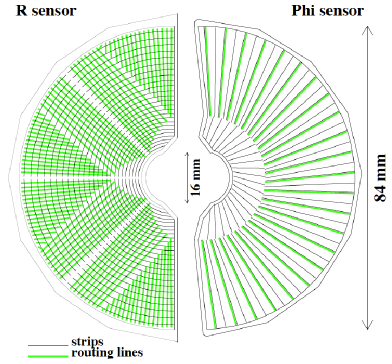
Each implant is read out via a capacitively coupled first metal layer running along its length. The R-type strips and inner -type strips do not extend to the outer region of the sensor. Therefore each strip is connected via a metal routing line to the edge of the sensor where the readout electronics are located. The routing lines are referred to as the second metal layer and are insulated from the bulk silicon and first metal layer by of . For R-type sensors, the routing lines are positioned perpendicular to the sensor strips, whilst for the -type they are positioned directly above and parallel to the strips.
| Parameter | Value |
|---|---|
| Silicon thickness | |
| Strip pitch | |
| Strip width | |
| Routing line width | |
| Inner silicon edge to beam axis | |
| Radial distance of active strips from beam axis | |
| Sensor position along beam-axis | |
| Oxygen enhancement |
This paper presents studies of radiation damage in the VELO sensors using data collected during and . Section 2 describes studies of sensor currents as a function of voltage and temperature. In section 3 the effects of radiation are monitored by measuring the charge collection efficiency and noise as a function of bias voltage. An unexpected decrease in clustering efficiency due to an effect involving the second metal layer is described in section 4. The results from the various studies are summarised in section 5.
2 Current evolution
The leakage current in a silicon sensor varies linearly with fluence for a wide range of silicon substrates [2]. This predictability provides a simple and accurate method of relating sensor currents to the amount of particle fluence accumulated by a sensor. This section presents an analysis of sensor currents in order to monitor radiation damage in the VELO.
2.1 Interpretation of sensor current measurements
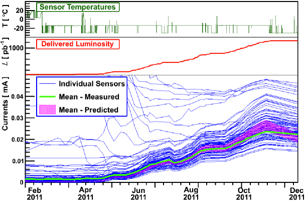
Each VELO sensor is biased through a high-voltage connection to the backplane, and a common ground connection to the bias line and innermost guard ring on the strip side. Therefore a single current is measured, corresponding to the current drawn by the entire sensor. The raw measured currents are shown as a function of time in figure 2, for sensors operated at the nominal bias voltage of and at a mean temperature of approximately . During the early running period, the majority of the sensors had small currents, with a few exceptions that had currents of up to . With sensor irradiation the bulk currents have increased. The spread of the measured currents is partly due to the difference in the sensor positions relative to the interaction point, but is dominated by variations in the sensor temperatures. The occasional dips in the currents are related to short annealing periods in which the cooling systems were switched off.
The measured currents contain contributions from two dominant sources, generically referred to as bulk and surface currents. The bulk currents vary exponentially with temperature and have a precisely predicted relationship with fluence. Surface currents arise due to irregularities introduced during sensor production such as process errors, scratches, guard rings and non-uniformities in the cut edges. Some of these contributions may have an exponential dependence on temperature [3], however the surface currents measured in VELO sensors are predominantly characterised by an Ohmic increase in current with bias voltage. In the majority of sensors the Ohmic surface current is seen to anneal with particle fluence. An analysis of VELO sensor currents as a function of bias voltage (IV scan) is described in detail in ref. [4].
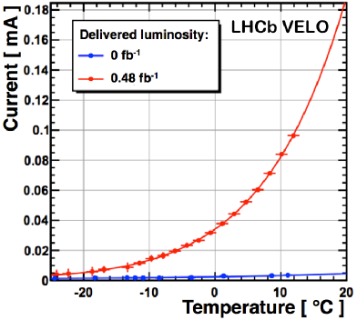
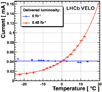
For the VELO sensors the pre-irradiation exponential contribution is very small and is assumed to consist of a mixture of bulk and surface currents. The relative contribution of bulk and surface current is identified by measuring the current as a function of temperature (IT scan), as shown in figure 3. This method is described in detail in ref. [5].
2.2 The effective band gap
In the temperature range of interest, the bulk current is expected to scale according to,
| (1) |
where is the temperature in Kelvin and is the Boltzmann constant (). The constant is related to the bandgap energy and an effective value of is assumed for the temperature range of interest [6]. Using this function the sensor currents can be normalised to a common temperature. In addition, the current variation as a function of temperature can be fitted to measure in the VELO sensors. A summary of the results obtained from several IT scans is presented in table 2. The statistical uncertainty quoted is the width of a Gaussian fitted to the distribution of the measured values from all sensors. The largest source of systematic uncertainty is related to the accuracy with which sensor temperatures are known, and the choice of the temperature fitting range [5].
| Delivered luminosity | Bias voltage | |
|---|---|---|
| [ V ] | [ eV ] | |
The weighted average of the measured values is , which is statistically compatible with the expected value of from the literature [6]. Recent studies [6] have shown that discrepancies can occur due to sensor self-heating, in which case is measured to be systematically high. In addition, dependencies of on the sensor bias voltage have been observed. However, the VELO sensors used for these measurements were cooled and sufficiently biased at V, such that these effects should not significantly influence the result. This is supported by the consistency of the cross-check measurement made at V.
2.3 Fluence determination
With a good understanding of the annealing conditions, changes in current can be related to the particle fluence incident on a sensor. The expected change in leakage current at room temperature is given by the relation,
| (2) |
where is the annealing parameter in units , is the fluence in units of number of particles per , and is the silicon volume in . The annealing parameter is a logarithmic function of time, and also depends on temperature. It has been shown to follow an Arrhenius relation,
| (3) |
where is the activation energy for which a value of has been derived from a fit [7]. In order to estimate the appropriate value of for our data, we proceed as follows. The sensor temperatures are recorded for each minute of operation and corrected to an equivalent time at . The delivered luminosity, , is folded with this equivalent time to produce an effective value of to be used in eq. 2. This procedure [5] yields a value for of , corresponding to an effective value for of .
Fluences simulated with GEANT4 in the LHCb detector are folded with particle damage factors using the NIEL scaling hypothesis [8]. The damage caused by high energy particles in the bulk material is parameterised as proportional to a displacement damage cross section, . A displacement damage cross section of MeV mb for MeV neutrons, , is assumed and each particle, , is assigned an energy-dependent hardness factor, ,
| (4) |
which can be used to estimate the damage in the material. The total damage is expressed as a multiple of the expected damage of a MeV neutron (referred to as MeV neutron equivalent, or MeV ). This technique has been shown to be highly effective for describing the evolution of the leakage current. For this analysis, every particle in the simulation that is incident on a VELO sensor is assigned a displacement damage cross-section, or cross-section per silicon atom, using as reference a set of tabulated values from ref. [9].
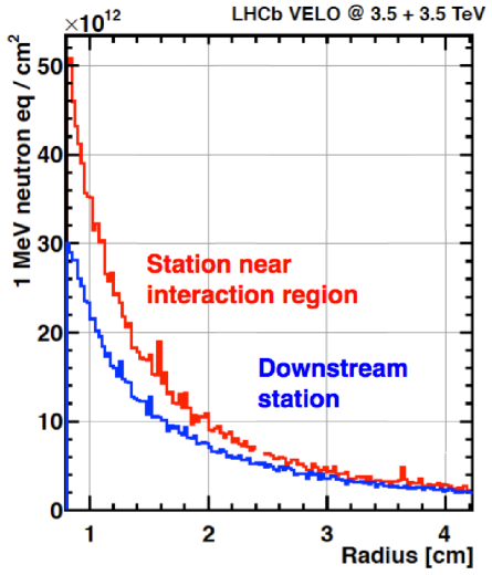
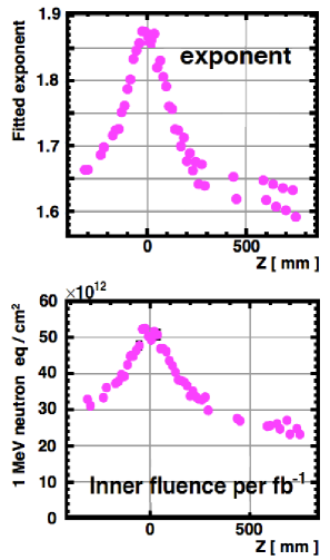
The fluence varies with the geometric location of the sensors in the VELO, as shown for simulated events in figure 4. It decreases with radial distance from the beam with an approximate dependence. The position along the beam-pipe (-direction) and path length of the particle in the silicon sensor were both found to significantly affect the fluence incident on a sensor. The predicted fluence is assigned an uncertainty of which is dominated by uncertainties due to particles with no available displacement damage data. The average measured current increase for the sensors at the operational temperature of approximately (and including several annealing periods) is A per .
2.4 Predicted currents
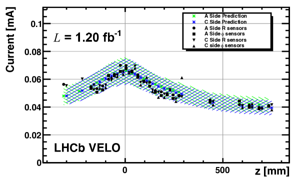
With the relationship between luminosity and damaging fluence established, the expected change in leakage current due to radiation damage can be predicted. The integrated luminosity is taken from the LHCb online measurement. Predictions are shown to agree with the measured currents, as shown in figure 5. The predictions have an associated uncertainty of approximately , estimated by adding the uncertainties for the integrated luminosity (), the annealing factor () and the damaging fluence prediction () in quadrature. The predicted leakage current is on average within of the measured current.
3 Depletion voltage studies
The depletion voltage, defined as the reverse bias voltage required to fully deplete a sensor, has been monitored as a function of the delivered luminosity. For fluences delivered to the VELO within the first few years of operation, the change in depletion voltage for an type sensor should be accurately described by the Hamburg model [10]. The effective doping of the -bulk changes over time due to radiation-induced defects. Dominant mechanisms are expected to be the inactivation of phosphorous dopants in combination with the introduction of acceptors. This leads to an initial decrease in the depletion voltage of the sensors to a value close to . The -type bulk inverts and becomes -type, after which further irradiation leads to an increase in depletion voltage. Eventually, the bias voltage required to obtain sufficient charge from a sensor will cause electrical breakdown in the silicon or exceed the V hardware limit, thus limiting the useful lifetime of the silicon detector. For an oxygenated type sensor irradiated with charged hadrons there are expected to be competing mechanisms, with acceptor introduction partially compensated by initial oxygen-induced acceptor removal [11, 12].
Following manufacture the depletion voltage of each VELO sensor was measured by comparing the capacitance (C) to the bias voltage (V) [13]. It is not possible to implement this technique after VELO installation and so alternative methods are used to extract information on the depletion voltage. This section presents results from two such studies: Charge Collection Efficiency and noise scan studies.
3.1 Charge Collection Efficiency
The amount of charge collected by an under-depleted silicon strip increases with the bias voltage applied. When the sensor is fully depleted, any further increase in bias voltage will not increase the amount of charge collected (given a sufficient signal collection time). The relationship between the Charge Collection Efficiency (CCE) and the applied bias voltage has been exploited to measure a property of the sensor analogous to the depletion voltage, referred to as the Effective Depletion Voltage (EDV).
3.1.1 Effective Depletion Voltage determination
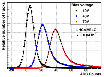
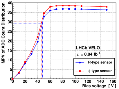
The nominal operational voltage of the VELO sensors is . For the CCE analysis, collision data is recorded with every fifth module operated at a voltage ranging between and . The remaining modules are maintained at . Sensors with variable voltage are referred to as test sensors. The test sensors are removed from the reconstruction algorithms such that only hits from the operated sensors are used to reconstruct particle tracks. A track is extrapolated to a coordinate on the test sensor and the set of five strips nearest to this coordinate are searched for deposited charge. This provides unbiased information on the amount of charge deposited by the particle as a function of bias voltage. At each bias voltage the pedestal-subtracted ADC distribution is fitted using a gaussian convoluted with a Landau function. This is used to determine the Most Probable Value (MPV) of the ADC distribution. At large bias voltages the MPV of the ADC distribution reaches a plateau. The EDV is defined as the voltage at which the MPV of a sensor is equal to of the plateau ADC value, as shown in figure 6. The threshold of was chosen as it gives closest agreement with depletion voltages determined from pre-irradiation CV measurements [13]. For unirradiated sensors, the difference in the values obtained using the CV method and the EDV method is less than .
Differences between the depletion voltage and EDV are expected near to sensor type-inversion. The depletion voltage is expected to decrease to a value of approximately V, whereas the minimum EDV is dictated by the smallest potential difference required to collect charge from the silicon strips, which in turn depends on the shaping time of the electronics. When operated with a ns signal shaping time, the smallest EDV that can be measured in the VELO sensors is approximately V. The EDV is therefore not an accurate estimate of the depletion voltage below this value.
3.1.2 Bulk radiation damage
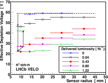
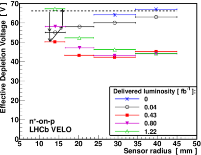
Between April and October five dedicated CCE scans were taken, corresponding to delivered luminosities of , , , and . As the fluence delivered to the sensors varies significantly with sensor radius, each sensor is divided into radial regions such that the fluence does not change by more than a factor of two across a region. The change in EDV with irradiation for a particular type sensor is shown in figure 7. Initially the EDV is found to decrease with fluence across all radial regions, as predicted by the Hamburg model. The rate of decrease is greater in the inner radial regions of the sensor, consistent with expectations that these regions are exposed to higher fluence. The innermost region undergoes an increase in EDV between and of delivered luminosity, indicating that this part of the sensor has undergone type inversion. The type sensors exhibit a decrease in EDV with initial fluence, as shown in figure 7. This is understood to be caused by oxygen induced removal of boron interstitial acceptor sites, an effect that has been previously observed [11, 12].
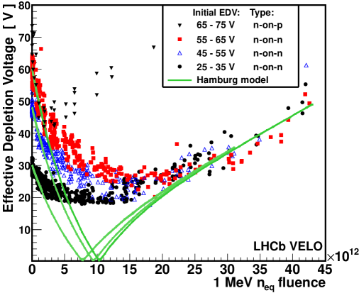
The global change in EDV is determined by combining the data from many of the VELO sensors with the predicted fluence (see section 2.3), as shown in figure 8. Sensors are divided into categories based on their initial EDVs. The irradiation-induced change in the depletion voltage of type sensors is modeled as a function of time, temperature and fluence by the Hamburg Model. It has three components: a short term annealing component, a stable damage component and a reverse annealing component. Taking into account the LHCb luminosity measurements and VELO sensor temperature readings, the Hamburg model predictions can be compared to data, as shown by the overlaid curves in figure 8. Good agreement is found for low fluences, and for higher fluences after type inversion. It is assumed that the sensors type invert at a fluence near to the EDV minimum. For all type sensors this occurs at approximately the same fluence of . The behaviour after inversion is found to be independent of the initial EDV of the sensor, with an approximately linear increase in EDV with further fluence. A linear fit to the data gives a voltage increase with fluence of . For the type, the initial decrease in EDV occurred up to a fluence of approximately . After this the EDV has increased with further fluence. The rate of increase is measured to be , similar to that of the type inverted type sensors.
The EDV of the type sensors begins to increase having received significantly less fluence than the type sensors. If the comparable rate of EDV increase is maintained with further fluence then the type sensors will reach an EDV of , the hardware limit of the VELO system, after receiving approximately less fluence than the type sensors. It is expected that the sensors will reach the limit following a fluence of approximately .
The amount of charge collected is expected to change with fluence due to radiation induced changes to the silicon. For -type sensors the MPV has decreased by approximately in the most irradiated regions, having received a fluence of . An even larger reduction of approximately is found in the inner regions of the R-type sensors, having received a comparable fluence. This is due to a charge loss mechanism related to the second metal layer of the R-type sensors, which is described in detail in section 4. The outer regions of the sensor are most significantly affected, with decreases of approximately observed following a fluence of just .
3.2 Noise scans
The CCE scan data described in section 3.1 requires proton beams, and so is collected at the expense of physics data. A second method has been developed to monitor radiation damage, using the relationship between the intrinsic electronic noise of the pre-amplifier and the capacitance of the sensor. Data scans for this study can be collected regularly as proton collisions are not required.
In undepleted silicon, several sources of input capacitance are identified, the most dominant of which is the inter-strip impedance. For sensors before type inversion, the depletion region grows with increasing voltage from the backplane (the opposite side to the strips). When the sensor is fully depleted the space-charge reaches the strips and the inter-strip resistance increases by several orders of magnitude, resulting in a decrease in sensor noise [14, 15]. For type sensors following type inversion and type sensors, the depletion region grows from the strip side of the silicon. In this situation the strips are immediately isolated at the application of a bias voltage and the relationship between noise and voltage cannot be exploited to extract information related to the depletion voltage.
The intrinsic noise in VELO sensors is determined by subtracting the mean ADC value (or pedestal) and a common-mode noise term. Figure 9 shows the inverse of the intrinsic noise as a function of voltage for an and type sensor.
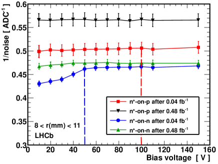
For the before and after irradiation, and after irradiation (having type inverted) the distribution is flat, thus little information related to the sensor depletion voltages can be extracted. For the type sensor prior to type inversion, an increase in voltage results in a decrease in noise until a plateau is reached when the sensor is fully depleted.
The noise scan data can be used to identify whether an type sensor has undergone type inversion. Only R-type sensors are investigated as the strip orientation allows the identification of strips that have been subject to a specific fluence. Following a delivered luminosity of approximately , of the sensors are identified as having type-inverted in the first radial region (), while in the second region () sensors are identified. Similar information can be extracted from the CCE data, with a sensor region defined as type-inverted when the measured EDV has reached a minimum and subsequently begun to increase. Following the same luminosity, the CCE method identified and type-inverted sensors in the first and second radial regions, considerably fewer than the noise method. This discrepancy is understood by examination of figure 8, in which the minimum of the Hamburg model prediction and the point at which the EDVs begin to increase are separated by a fluence of approximately . The noise scan method is not subject to the same fluence lag. Following a delivered luminosity of , the CCE method identifies and sensors in the two radial regions. This is in good agreement with the noise method, with the same and sensors identified by each method.
4 Charge loss to the second metal layer
All physics analyses at LHCb rely on efficient track reconstruction using clusters from the VELO sensors. A cluster is defined as one or several adjacent strips with charge above a particular threshold. The data samples described in section 3.1 are also used to measure the Cluster Finding Efficiency (CFE), by looking for the presence of a cluster at the track intercept on the test sensor. Before irradiation the mean CFE of the VELO sensors was greater than [16]. After irradiation the CFE in many sensors decreased significantly, as shown in figure 10. The inefficiency is particularly prevalent at large sensor radii and for high bias voltages.
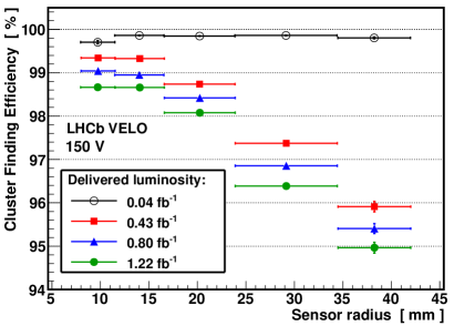
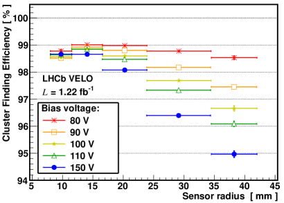
The decrease in CFE does not appear to be proportional to the delivered luminosity, but instead exhibits a rapid drop between the and data scans.
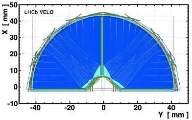
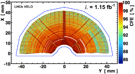
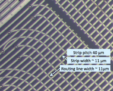
To determine the source of this CFE decrease, a large sample of regular LHCb physics data has been used to measure the CFE for small spatial regions on a sensor at the nominal bias. The result of this is shown in figure 11, displayed beside a diagram illustrating the layout of the second metal layer readout lines. There is a clear correspondence between the two figures, with high CFE measured in regions that are devoid of second metal layer lines. The relative orientation of the strips and routing lines in R-type sensors is shown in figure 12. In addition, a schematic cross-section of an R-type sensor is shown in figure 13. The routing lines from inner strips are seen to pass approximately perpendicularly over the outer strip implants.

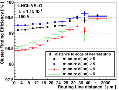
Using the precision tracking of the VELO, it is possible to investigate the CFE loss as a function of the distance between a track intercept with a sensor, and the nearest strip and routing line. This is shown in figure 14. The CFE is improved for track intercepts that are near to the strip implants. Conversely, the CFE is reduced when a track intercept is far from a strip and near to a routing line. Similar effects have been observed in other experiments [17, 18].
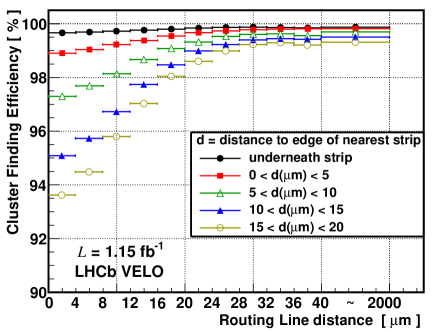
The source of the CFE loss is hypothesised in terms of charge induction on the second metal layer. Prior to irradiation, ionised electrons will drift along the field lines, most of which terminate at the implants. Hence the majority of the signal will be induced on the implants, which are strongly capacitively coupled to the readout strips. The drifting charge is expected to be collected well within the ns readout period of the electronics, and no signal is expected on neighbouring electrodes (with the exception of capacitive coupling and cross-talk effects, which are measured to be low). However, irradiation may cause modifications to the field line structure, such that not all field lines terminate on the implants. In addition, there may be charge trapping effects which delay the drift of charge, resulting in charge sampling before the electrons have reached the implants. In both of these situations there will be a net induced charge on nearby electrodes, such as the second metal layer routing lines. In figure 10 the CFE was seen to worsen with increasing bias voltage. This appears to disfavour the contribution due to trapping, as an increase in bias voltage should result in faster collection times. However, the bias voltage may also affect the field-line structure. In reality, it is likely that the charge loss to the second metal layer is due to several competing mechanisms.
The CFE loss also exhibits a significant radial dependence, as was shown by figure 10. This can be understood by considering two competing mechanisms. The implant strip width and the fractional area covered by the strips increases with radius, resulting in reduced charge loss, due to greater strip shielding. However, the fractional area covered by the second metal layer also increases with radius, due to the greater density of lines, increasing the amount of pickup. The latter effect is dominant, hence the overall charge loss is greater at large sensor radii.
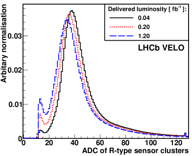
In addition to lowering the clustering efficiency, charge induced on a routing line can introduce a noise cluster. The cluster ADC distribution from R-type sensors has a peak associated to these low ADC noise clusters that has grown with fluence, as shown in figure 15. These noise clusters are predominantly single strip clusters located at small radius regions of R-type sensors. The fraction of the induced noise clusters increases when tracks traverse a sensor near to a routing line and far from a strip, as shown in figure 15.
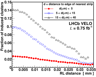
The CFE decrease is not observed in -type sensors as the routing lines from inner strips were intentionally placed directly above the outer strips to minimise pick-up. This is made possible by the -type sensors strip orientation. The CFE loss could be partially recovered by lowering the cluster reconstruction thresholds. However this comes at the expense of a worse signal to background ratio which leads to higher rates of fake tracks reconstructed from noise induced clusters.
The R-type and sensors have a similar CFE dependence on the strip and routing line distance, as shown in figure 16. Figure 16 shows the MPV of the collected charge distribution as a function of bias voltage for an and an type sensor. At , the MPV of the and are approximately equal, both before and after irradiation. For the type sensor post irradiation, the MPV reaches a maximum at around after which it is observed to decrease with increasing bias voltage. This decrease in MPV leads to a reduced CFE and is associated with the second metal layer effect. Therefore less charge is lost to the second metal layer when operating the sensor at a lower than nominal voltage.
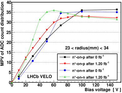
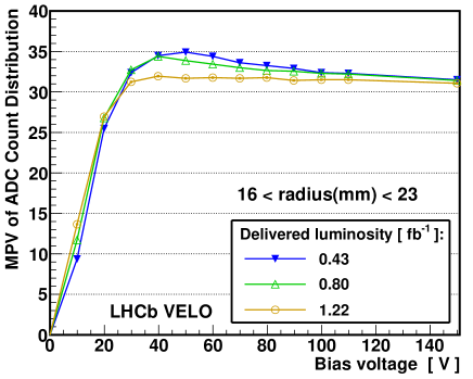
The type sensor does not exhibit this same charge collection loss (and resulting CFE decrease) dependence on voltage. This may be due to the depletion region in the type sensor growing from the strip side of the silicon instead of from the sensor backplane. This is supported by the observation that after type inversion, charge loss in type sensors no longer depends on the bias voltage, as shown in figure 17.
5 Summary
The effects of radiation damage have been observed in all of the LHCb VELO sensors. At the operational sensor temperature of approximately , the average rate of sensor current increase is measured to be per , in agreement with expectations. The silicon effective bandgap has been determined using current versus temperature scan data collected at various levels of radiation, with an average value of found.
Analysis of the Charge Collection Efficiency has proven an effective method for tracking the evolution of the sensor depletion voltages with fluence. Measurements of the Effective Depletion Voltage after sensor type inversion have been shown to agree well with the Hamburg model predictions. A method relating the sensor noise dependence on bias voltage was used to identify type-inverted sensors, and was found to be in good agreement with the Charge Collection Efficiency method.
A significant decrease in the Cluster Finding Efficiency in R-type sensors due to the second metal layer has been observed following a relatively small amount of particle fluence. In the worst affected sensor regions the Cluster Finding Efficiency decreased by over . Despite this relatively large localised inefficiency, studies of the VELO tracking efficiencies show no degradation associated to this effect, within the errors of . For the type sensors before type inversion the magnitude of the charge loss is found to increase with sensor bias voltage. For type-inverted type sensors and type sensors, a voltage dependence is not observed. Radiation induced modifications to the field line structure and charge trapping effects are thought to be possible sources of this charge loss effect.
The two sensors have been studied in detail, providing valuable information for upgraded detector designs. If the Effective Depletion Voltage were to continue increasing at the currently observed rate with further irradiation, then the would reach the V hardware limit having received approximately less fluence than an equivalent type sensor. This corresponds to approximately of integrated luminosity in the highest particle fluence region of the VELO.
Acknowledgements
We express our gratitude to our colleagues in the CERN accelerator departments for the excellent performance of the LHC. We thank the technical and administrative staff at the LHCb institutes. We acknowledge support from CERN and from the national agencies: CAPES, CNPq, FAPERJ and FINEP (Brazil); NSFC (China); CNRS/IN2P3 and Region Auvergne (France); BMBF, DFG, HGF and MPG (Germany); SFI (Ireland); INFN (Italy); FOM and NWO (The Netherlands); SCSR (Poland); ANCS/IFA (Romania); MinES, Rosatom, RFBR and NRC “Kurchatov Institute” (Russia); MinECo, XuntaGal and GENCAT (Spain); SNSF and SER (Switzerland); NAS Ukraine (Ukraine); STFC (United Kingdom); NSF (USA). We also acknowledge the support received from the ERC under FP7. The Tier1 computing centres are supported by IN2P3 (France), KIT and BMBF (Germany), INFN (Italy), NWO and SURF (The Netherlands), PIC (Spain), GridPP (United Kingdom). We are thankful for the computing resources put at our disposal by Yandex LLC (Russia), as well as to the communities behind the multiple open source software packages that we depend on. A special acknowledgement goes to all our LHCb collaborators who over the years have contributed to obtain the results presented in this paper.
References
- [1] LHCb collaboration, A. A. Alves Jr. et al., The LHCb detector at the LHC, JINST 3 (2008) S08005
- [2] M. Moll, Radiation Damage in Silicon Particle Detectors - microscopic defects and macroscopic properties, PhD thesis, Fachbereich Physik der Universität Hamburg, 1999
- [3] Y. Wang, A. Neugroschel, and C. T. Sah, Temperature Dependence of Surface Recombination Current in MOS Transistors, IEEE Trans. Nucl. Sci. 48 (2001) 2095
- [4] A. Gureja et al., Use of IV (current vs voltage) scans to track radiation damage in the LHCb VELO, LHCb-PUB-2011-020
- [5] A. Hickling et al., Use of IT (current vs temperature) scans to study radiation damage in the LHCb VELO, LHCb-PUB-2011-021
- [6] A. Chilingarov, Generation current temperature scaling, Tech. Rep. PH-EP-Tech-Note-2013-001, CERN, Geneva, Jan, 2013
- [7] E. Fretwurst et al., Reverse annealing of the effective impurity concentration and long term operational scenario for silicon detectors in future collider experiments, Nucl. Instrum. Meth. A342 (1994), no. 1 119
- [8] A. Vasilescu, The NIEL hypothesis applied to neutron spectra of irradiation facilities and in the ATLAS and CMS SCT, ROSE/TN/97-2, December, 1999
- [9] A. Vasilescu and G. Lindstroem, Displacement damage in silicon, on-line compilation, tech. rep., http://sesam.desy.de/members/gunnar/Si-dfuncs.html
- [10] R. Wunstorf et al., Results on radiation hardness of silicon detectors up to neutron fluences of , Nucl. Instrum. Meth. A315 (1992), no. 1–3 149
- [11] F. Lemeilleur et al., Electrical properties and charge collection efficiency for neutron-irradiated p-type and n-type silicon detectors, Nuclear Physics B - Proceedings Supplements 32 (1993), no. 0 415
- [12] M. Lozano et al., Comparison of radiation hardness P-in-N, N-in-N, N-in-P Silicon Pad Detectors, IEEE Trans. Nucl. Sci. 52 (2005) 1468
- [13] P. R. Turner, VELO module production - sensor testing, LHCb-2007-072
- [14] The CMS Tracker Collaboration, C. Barth, Evolution of silicon sensor characteristics of the CMS tracker, Nucl. Instrum. Meth. A658 (2011), no. 1 6
- [15] The CMS Tracker Collaboration, C. Barth, Evolution of silicon sensor characteristics of the CMS silicon strip tracker, Nucl. Instrum. Meth. In Press (2012), no. 0
- [16] The LHCb VELO Group, Perfomance of the LHCb Vertex Locator, To be submitted to JINST (2012)
- [17] ATLAS Pixel Collaboration, L. Tommaso, Test beam results of ATLAS Pixel sensors, arXiv:hep-ex/0210045
- [18] T. Rohe et al., Position Dependence of Charge Collection in Prototype Sensors for the CMS Pixel Detector, IEEE Trans. Nucl. Sci. 51 (2004) 1150