Numerical formulation of three-dimensional scattering problems for optical structures
Abstract
This paper describes a numerical formulation for calculating wave propagation with high precision in a three-dimensional system. Yee’s discretization scheme is used to formulate a frequency domain method that is compatible with the finite-difference time-domain (FDTD) procedure. When the S-matrix satisfies a unitarity (power flow conservation) condition, the method enables arbitrary S-matrix elements to be obtained within a numerical error of less than () for double precision format.
pacs:
02.60.Cb,41.20.Jb,42.15.Eq,42.25.BsI introduction
Numerical simulations are important for studying electromagnetic-wave propagation in optical physics Joannopoulos and for designing silicon photonics Kimerling ; Miller .
One of the most successful numerical methods is the finite-difference time-domain (FDTD) method 198008_taflove .
It is suitable for visualizing dynamical propagation of electromagnetic waves.
Simulations should not only give us a general understanding of the propagation, but also the details of the optical scattering.
Designing chips such as silicon optical interposers Urino requires highly precise simulations including the transmittance and reflectance of the fundamental and higher order modes at each wavelength (i.e., each frequency).
Small reflections may cause substantial instability Yamamoto between devices on the optical chip, and the small losses that result may build up (e.g. see Table I in Ref. Urino ).
Thus, we need a way to confirm that the numerical results are precise when the scattering properties are simulated.
Here, we should note that the precision of a numerical calculation, which is affected by both numerical method (e.g. numerical stability for the FDTD Taflove_book ) and numerical implementation (e.g. floating-point arithmetic IEEE754 ), is essentially different from the accuracy of numerical modeling that includes both the choice of the fundamental equation (e.g. microscopic nonlocal approach Cho is one such choice) and the discretization of the numerical procedure (e.g. numerical dispersion for the FDTD Taflove_book ).
In a scattering simulation, the error related to the accuracy is often explicit and predictable, but the error related to the precision is apt to be implicit and unforeseeable.
The S-matrix approach Wheeler is widely used to study scattering problems Buttiker , and numerical S-matrices have already been applied to scattering simulations on photonic crystal slabs Tikhodeev ; Li ; Liscidini and metal films Anttu .
Unfortunately, no method as yet has been discussed related to highly precise simulations in the three-dimensional optical structures.
This paper proposes a numerical method that can produce precise S-matrices for designing the silicon photonics devices.
The method exploits a numerical procedure for quantum transport Usuki ; Akis .
The numerical precision of the method is evaluated in terms of the S-matrix properties.
II Formulation
Consider the macroscopic Maxwell equations in the angular frequency domain ( space),
| (1) |
where () is vacuum permittivity (permeability). The symbol denotes an imaginary number, and the notation “” describes a harmonic oscillation.
The symbols , , , , and in the following formulation denote integers.
Instead of using dipole moments in the optical media, Eqs. (1) are used to express the relative permittivity and relative permeability .
Note that
for absorbing media.
The optical system in Fig. 1 consists of three parts: two ideal waveguides and a region with scattering and absorption.
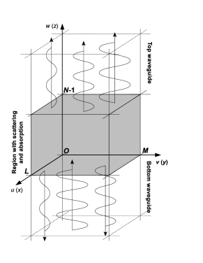
The coordinates in Fig. 1 are ones transformed using , and they are used to apply a non-uniform mesh to Eqs. (1). Note that the Jacobian matrix of this transformation is diagonal in order to simplify the discussion in the following subsections -.
II.1 Discrete representation
Let us discretize the transformed space: , and let us use cells in Yee’s lattice Yee .
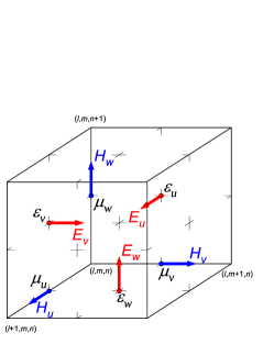
Figure 2 shows an arrangement of discretized functions (, , and ) that are allocated a cell address . For example, the component of the magnetic field means at , , in the figure. The electromagnetic field in coordinates is related to that of the coordinates in the following manner.
| (2) |
and
| (3) |
where , , and are defined as
| (4) |
Here, is the velocity of light in a vacuum. We make the domain of variables and finite: and , where the boundaries and are integers. Furthermore, and for in Fig. 2 are defined as
and
The relative permittivity and relative permeability for satisfy periodic conditions, i.e., and .
The six components of the electromagnetic field satisfy the following conditions:
where , for . The parameters , are generally complex numbers, and they satisfy . In this paper, . Now let us introduce the forward difference operators,
| (5) |
At and , and are defined as
The backward difference operator is , where “T” denotes the transpose. Using Eqs. (4) and (5), we can define modified difference operators:
| (6) |
From Eqs. (1) and (6), the and components of the electromagnetic field satisfy
| (7) |
with the matrices,
| (8) |
and the diagonal matrices,
The column vectors and in Eq. (7) are expressed as
Here,
From Eqs. (1), the -components in Eqs.(2) and in Eqs.(3) can be expressed as
II.2 Wave propagation in ideal waveguides
For the bottom ideal waveguide, , of Eqs. (8) and in Eqs. (4) are
For the top ideal waveguide, they are
Since the permittivity in the ideal waveguides is real, we have
| (9) |
for . Figure 4 depicts the arrangement of the above equations.
The eigenvalue equation for the optical modes of the ideal waveguides is
| (10) |
for . Here, are eigenvectors. Appendix B show that all eigenvectors satisfy
| (11) |
where is Kronecker’s delta. The propagation constants and are given by
| (12) |
and . We use an integer to separate the propagating modes and evanescent modes of the above : as , and as . We build a square matrix consisting of the eigenmodes of Eq. (10), a diagonal matrix from Eq. (12) consisting of the phases of the modes, and column vectors consisting of the coefficients of the -th mode in the waveguides:
| (13) |
Note that from Eq. (11). The and in the bottom ideal waveguide are defined by using Eq. (13):
| (14) |
The and in the top ideal waveguide are defined in the same manner.
II.3 Power flow with absorption
Let us define the discretized formulation of time averaged power flowOkamoto :
| (15) |
where “†” denotes the Hermitian conjugate. From Eqs. (12), (13) and (14), the power flows and for Eq. (15) are given by
| (16) |
where is real and positive. Equations (7), (15), and (16) lead to the following relation between power flow and absorption:
II.4 Transfer matrices
We make column vectors of the electromagnetic modes and matrices , which we call transfer matrices: . The are defined as
Equations (7) and (14) yield the transfer matrices:
| (18) |
For , we have
| (19) |
By using Eqs. (18) and (19), we can obtain the matrices and from the linear equation:
| (20) |
which is the same as Eq. (2.17) in our previous study Usuki .
II.5 Stable transfer matrix method
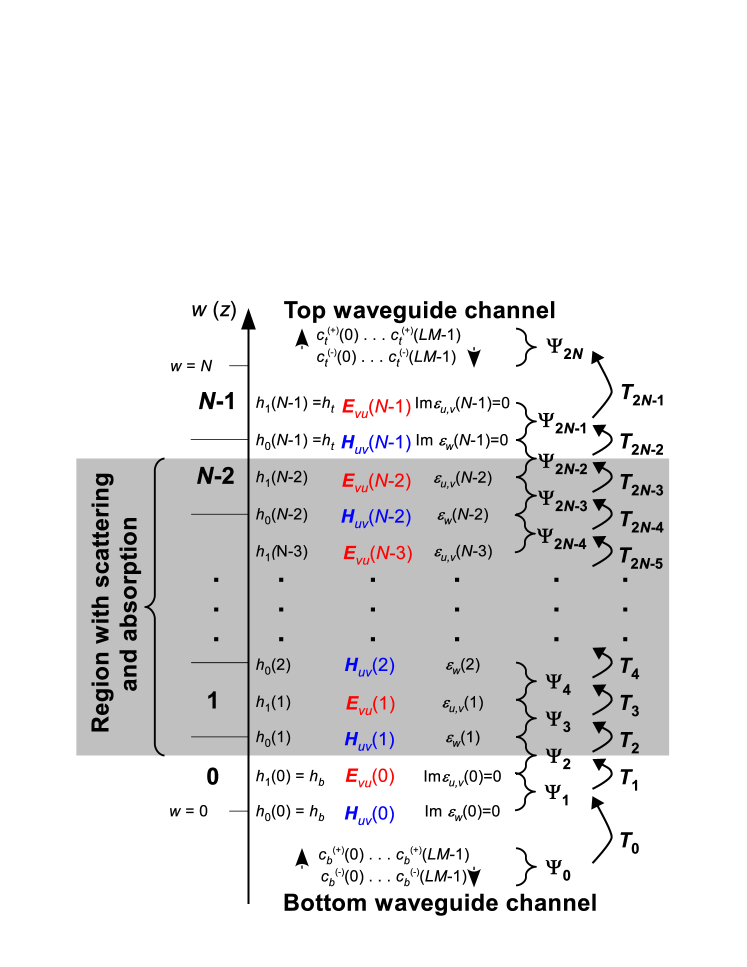
To solve the above Eq. (20), we can establish a stable iterative procedure Usuki ; Akis by using the column operator . This procedure does not entail solving multi-slice eigenvalue problems for the region with scattering and absorption, which has advantages in both computational time and numerical precision over the other procedure Ko ; Usuki94 that can be applied to optical scattering Tikhodeev ; Li ; Liscidini ; Anttu . In the following discussion, suppose we have blocks of matrices and notated by
The iterative equations for the matrix and the matrix can be used to find and :
| (21) |
The initial conditions are that
| (22) |
always satisfies
because of the column operator in Eq. (21). has the following matrix representation:
| (28) | |||||
and here, the actual numerical procedure uses Gaussian elimination without partial pivoting for . From Eqs. (22) and (28), we find that iterating Eq. (21) gives us
We can compute the electromagnetic field in the scattering region by making matrices for and for for the -th cell. The initial conditions are
for . The and are iterated using the column operator :
Appendices C and D give two approaches to simulating the reverse scattering process from the top ideal waveguide to the bottom ideal waveguide. We can use either of these approaches to obtain , , and for the reverse process.
II.6 Scattering matrix
Let us define a matrix and a matrix only for propagating wave modes. The elements of and are normalized to and by the power flow of Eq. (16) as follows:
If we only obtain the matrices and , we can reduce the matrix sizes of and : blocks and , blocks and , a block , and a block . By using the matrices and , we can define a matrix and a matrix . In so doing, we obtain a S-matrix Buttiker :
| (29) |
Let us define matrices ,
and matrices , only for propagating wave modes. We also define a matrix and a matrix
| (30) |
From Eqs. (II.3) and (30), the S-matrix including the case of absorption media satisfies
| (31) |
This equation shows that the S-matrix is unitary when for .
III Numerical results
The method described in the previous section is suitable for analyzing very small scattering coefficients.
Here, we will discuss the optical properties of a sidewall grating waveguide (SGW) that is part of a phase shifter in a silicon optical modulator Akiyama .
The grating structure is used to inject free carriers into the waveguide core, but for it to work properly, the reflections of the fundamental mode and radiation loss from the structure have to be suppressed.
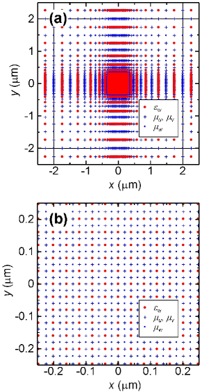
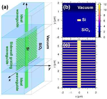
Figure 5 shows the SGW and its permittivity Tong distribution.
The SGW is a silicon waveguide and has a cladding layer on which a vacuum region is set.
For the numerical analysis, we set the waveguide core to and the grating pitch (width) to 284 (74.5) nm.
Before conducting the simulation, we have to obtain optical modes for the ideal waveguides at both ends of the SGW. The ideal waveguides have three waveguide modes and many radiation modes, as shown in Fig. 6.
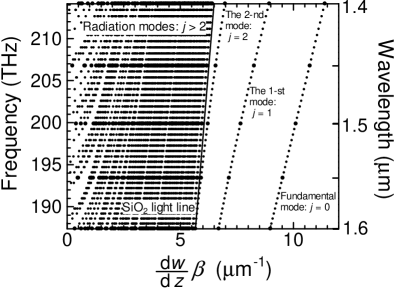
The propagating mode numbers and are that at , because we set four periodic boundary conditions along the and axes. The grid parameters of and are the same as in Fig. 3, whereas the grid parameters of are and . Figure 7 shows cross sections of the waveguide modes and radiation modes at a wavelength of 1.55 .
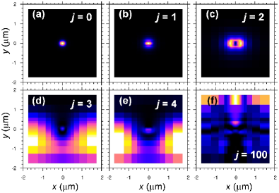
The three waveguide modes in Fig. 7(a)-(c) are labeled , and Okamoto .
The waveguide modes are clearly localized around the silicon waveguide core.
From the -axis symmetry of the SGW, the fundamental mode scattering through the SGW is intra-mode scattering (i.e. reflection) when the scattering only occurs between the waveguide modes.
However, the scattering process between the and radiation modes is complex.
Figure 7(d)-(f) shows three of the 100 radiation modes.
The optical power outside the core is dominant for each radiation mode, but remains small inside the core.
Therefore, we have to consider not only the reflection within the but also scattering between and other modes including radiation modes.
Figure 8 shows the transmittance and reflectance of the SGW when is launched from the bottom.
There is a stop band at around , after which the fundamental-mode reflectance decreases with a periodic modification of increasing wavelength.

The reflectance of each radiation mode also has a strong wavelength dependence. In particular, it has a low value at the point of the third mode reflectance in Fig. 8.
The total optical loss, which is caused by reflection and radiation-mode scattering, is () at a wavelength of .
Note that the loss does not have so strong a wavelength dependence.
The simulation results clearly show that the sidewall grating does not cause significant losses or reflections for the silicon optical interposer Urino .
In an actual phase shifter Akiyama , the gratings on either side of the waveguide core are doped with donors or acceptors, and aluminum electrodes are attached to the gratings (see Fig. 9).
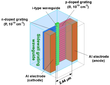
Doped silicon Soref ; Reed with metal electrodes Shiles ; Ordal changes the optical index and absorption properties of the SGW. We calculated the scattering process for absorption at a wavelength of . Figure 10 shows the distribution of and as .
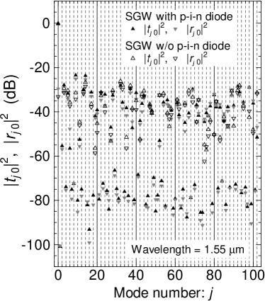
The total optical loss is (), and it consists of reflection (see the case of in Fig. 10), scattering (), radiation-mode scattering (), and absorption loss ( ()). Note that the distribution around and the scattering are caused by an -axis asymmetry due to the different optical indexes of the p-doped and n-doped regions Soref ; Reed .
IV Conclusions
This proposed method can calculate scattering coefficients for all incident modes from the bottom waveguide and the top waveguide. To determine the precision numerically, we use the max norm on the left side of Eq. (31):
| (32) |
and the max norm on the left side of Eq. (11) for the propagation modes:
| (33) | |||||
We can estimate the numerical error of the obtained scattering coefficients by performing a double precision calculation of Eqs. (32) and (33). Figure 11 shows that numerical error of the eigenvalue calculation for ideal waveguide modes causes error.

Using the Type I reverse propagation described in Appendix C results in an value of less than .
On the other hand, the numerical error of the power-flow conservation for scattering does not depend on , and it is less than , as shown in the inset of Fig. 11.
Therefore, our method satisfies the condition placed on the S-matrix (Eq. (32)) and gives us detailed optical properties with high enough precision for designing silicon photonics devices Urino ; Akiyama .
For typical simulations, we recommend the Type II in Appendix D, because it takes only about half of the computational effort of Type I.
We will use this method to analyze low and complex optical scattering cases.
Furthermore, the discretization of the permittivity distribution on the Yee lattice is compatible with FDTD.
By combining this method and FDTD, numerical analyses with an optical propagation model can be made general and detailed.
Acknowledgements.
The author would like to thank Makoto Okano for telling me about the FDTD method, Suguru Akiyama and Takeshi Baba for their fruitful discussions on Sec. III of this paper, and Motomu Takatsu for his helpful comments on Appendix B. This work was supported by the “Funding Program for World-Leading Innovative R&D on Science and Technology (FIRST Program).”Appendix A Non-uniform mesh for equations (4)
Here, we show the details of the coordinate transformation. The periodic boundary conditions should be applied to and :
We introduce the periodic function into and .
| (34) |
The function (34) has several properties:
where is the Dirac delta function. From Eq. (34), we obtain an analytical formula for the integral of .
| (35) |
The integral of has a staircase shape. For example, we can set and by using
| (36) |
given ten parameters , , , , , , , and .
Appendix B Orthogonality of eigenvalue equation (10)
We should note that , where “†” denotes the Hermitian conjugate, when , and that no linear combination (real ) is positive definite. However, the eigenvector still satisfies
As an example, let us consider a simple equation, , where the matrix is not positive definite. This equation has complex eigenvalues and eigenvectors: , , and
Therefore, we can normalize all eigenvectors as
when eigenvalues are non-zero and non-degenerate, and number of eigenvalues is equal to the order of .
The eigenvalue equations for the numerical results of Sec. III satisfy this condition.
We recommend checking which eigenvalue equations satisfy the condition or not, because there exists a counter example: .
This equation has only one linearly independent eigenvector and
Accordingly, we should carefully normalize eigenvectors when the equation does not satisfy the condition.
Appendix C Reverse propagation type I
For reverse propagation in the same framework as that of forward propagation, we define a column vector as
The transfer matrix , which satisfies , is defined as
for ,
and
The reverse equation corresponding to the forward Eq. (20) is
Reverse iteration is defined as
with initial conditions,
The column operator can be defined in the same manner as Eq. (28); that is,
without . and are
because () is different from (). Here,
Thus,
and
Furthermore,
Thus,
From Eqs. (19), is an expression similar to . Reverse iteration yields
At the -th cell, we can introduce and . For , the initial conditions are
The following iterations derive and :
Appendix D Reverse propagation type II
We can derive another equation for and :
At the step, we introduce and :
Thus,
| (51) |
Note that , and for . The iterative procedure of Eq. (51) yields
We can add and to the step.
Finally, we obtain
References
- (1) J. D. Joannopoulos, S. G. Johnson, J. N. Winn, and R. D. Meade “Photonic Crystals,” 2nd-ed., Princeton University Press (2008).
- (2) L. C. Kimerling, D. Ahn, A. B. Apsel, M. Beals, D. Carothers, Y.-K. Chen, T. Conway, D. M. Gill, M. Grove, C.-Y. Hong, M. Lipson, J. Liu, J. Michel, D. Pan, S. S. Patel, A. T. Pomerene, M. Rasras, D. K. Sparacin, K.-Y. Tu, A. E. White, and C. W. Wong, Proc. SPIE 6125, 612502-1 (2006).
- (3) D. A. B. Miller, Proc. IEEE 97, 1166 (2009).
- (4) A. Taflove, IEEE Transactions on Electromagnetic Compatibility, EMC-22, 191 (1980).
- (5) Y. Urino, Y. Noguchi, M. Noguchi, M. Imai, M. Yamagishi, S. Saitou, N. Hirayama, M. Takahashi, H. Takahashi, E. Saito, M. Okano, T. Shimizu, N. Hatori, M. Ishizaka, T. Yamamoto, T. Baba, T. Akagawa, S. Akiyama, T. Usuki, D. Okamoto, M. Miura, J. Fujikata, D. Shimura, H. Okayama, H. Yaegashi, T. Tsuchizawa, K. Yamada, M. Mori, T. Horikawa, T. Nakamura, and Y. Arakawa, Opt. Express 20, B256 (2012).
- (6) T. Yamamoto, H. Kobayashi, M. Ekawa, S. Ogita, T. Fujii, T. Higashi and M. Kobayashi, Electronics Lett. 33, 65 (1997).
- (7) Chapter 4 in A. Taflove and S. C. Hagness, “Computational Electrodynamics: The Finite-Difference Time-Domain Method,” 2nd-ed., Artech House (2000).
- (8) IEEE, “IEEE standard Floating-Point Arithmetic,” IEEE Std 754-2008, pp. 1-58, Aug 2008.
- (9) K. Cho, “Optical Response of Nano-structures: Microscopic Nonlocal Theory,” Springer Verlag, Heidelberg (2003); Errata, Web site of Springer Verlag for this book.
- (10) J. A. Wheeler, Phys. Rev. 52, 1107 (1937).
- (11) M. Büttiker, Y. Imry, R. Landauer, and S. Pinhas, Phys. Rev. B 31, 6207 (1985).
- (12) S. G. Tikhodeev, A. L. Yablonskii, E. A. Muljarov, N. A. Gippius, and T. Ishihara, Phys. Rev. B 66, 045102 (2002).
- (13) Z.-Y. Li and L.-L. Lin, Phys. Rev. E 67, 046607 (2003).
- (14) M. Liscidini, D. Gerace, L. C. Andreani, and J. E. Sipe, Phys. Rev. B 77, 035324 (2008).
- (15) N. Anttu and H. Q. Xu, Phys. Rev. B 83,165431 (2011).
- (16) T. Usuki, M. Saito, M. Takatsu, R. A. Kiehl, and N. Yokoyama, Phys. Rev. B 52, 8244 (1995).
- (17) R. Akis and D. Ferry, J. Comput. Electron. 9, 232 (2010).
- (18) K. S. Yee, IEEE Trans. Antennas Propag. AP-14, 302 (1966).
- (19) Equation (1.44) and Fig. 2.11 in K. Okamoto, “Fundamentals of Optical Waveguides,” 2nd-ed., Elsevier Inc. (2006).
- (20) D. Y. K. Ko and J. C. Inkson, Phys. Rev. B 38, 9945 (1988).
- (21) T. Usuki, M. Takatsu, R. A. Kiehl, and N. Yokoyama, Phys. Rev. B 50, 7615 (1994).
- (22) S. Akiyama, T. Baba, M. Imai, T. Akagawa, M. Takahashi, N. Hirayama, H. Takahashi, Y. Noguchi, H. Okayama, T. Horikawa, and T. Usuki Opt. Express 20, 2911 (2012).
- (23) Equations (6) and (7) in L. Tong, J. Lou, and E. Mazur, Opt. Express 12, 1025 (2004).
- (24) “ITU-T G.694.2,” http://www.itu.int/rec/T-REC-G.694.2-200312-I/en
- (25) R. A. Soref, and B. R. Bennett, IEEE J. Quantum Electron., QE23, 123 (1987).
- (26) G. T. Reed, G. Mashanovich, F. Y. Gardes and D. J. Thomson, nature photonics 4, 518 (2010).
- (27) E. Shiles, T. Sasaki, M. Inokuti and D. Y. Smith, Phys. Rev. B 22, 1612 (1980).
- (28) Table 1 in M.A. Ordal, L. L. Long, R. J. Bell, S. E. Bell, R. R. Bell, R. W. Alexander, Jr. and C. A. Ward, Appl. Opt. 22, 1099 (1983).