Antiferromagnetic Domain Structure in Bilayer Manganite
Abstract
We report a novel soft x-ray nanodiffraction study of antiferromagnetic domains in the strongly correlated bylayer manganite La0.96Sr2.04Mn2O7. We find that the antiferromagnetic domains are quenched, forming a unique domain pattern with each domain having an intrinsic memory of its spin direction, and with associated domain walls running along crystallographic directions. This can be explained by the presence of crystallographic or magnetic imperfections locked in during the crystal growth process which pin the antiferromagnetic domains. The antiferromagnetic domain pattern shows two distinct types of domain. We observe, in one type only, a periodic ripple in the manganese spin direction with a period of approximately 4 µ m . We propose that the loss of inversion symmetry within a bilayer is responsible for this ripple structure through a Dzyaloshinskii-Moriya-type interaction.
There are two main classes of magnetic ordering: ferromagnetism and antiferromagnetism. Both types are exploited in technological devices and find numerous applications. In both cases, the local order forms microscopic domains. While ferromagnetic (FM) domain formation is well understoodHubert and Schaefer (1998); Neel (1955); Landau et al. (1984), antiferromagnetic (AFM) domains remain mysterious mostly due to a lack of techniques which can spatially resolve the AFM order. This is unfortunate, since antiferromagnetism is an ubiquitous magnetic ordering important for both fundamental research and practical applications. It is used to pin ferromagnetic layers in exchange bias systemsScholl et al. (2000); Nogues et al. (2005) and can cause spin-valve-like behavior in multilayers of an AFM layer and a non-magnetic layerPark et al. (2011). From a fundamental physics perspective, it is also one of the most common ground states in condensed matter physics, especially in transition metal oxides. A prominent example being AFM stripe order in doped, superconducting cupratesTranquada et al. (2008). Further, AFM domains play an important role in defining the operation of any device. For example, in nanoscaled exchange bias systems they determine the strength of the exchange bias Mauri et al. (1987); Malozemoff (1987); Miltenyi et al. (2000); Nowak et al. (2002). Antiferromagnets, unlike ferromagnets, have no net demagnetizing field and therefore the formation of domains is not required by energy considerations, although one could argue that entropy suggests their presence. Basic questions therefore remain to be answered, including the size and structure of AFM domains and if they are quenched, or if they can easily be annealed.
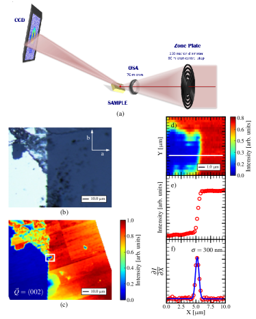
The study of AFM domains is extremely challenging. The absence of any net magnetic moment prohibits the use of most magnetic imaging techniques. Recently, Photoemission Electron microscopy (PEEM) combined with X-ray Magnetic Linear Dichroism (XMLD) has been used to image AF domains Stoehr et al. (1999); Scholl et al. (2000). Here we present the novel technique of soft x-ray resonant nano diffraction, which has considerable advantages over PEEM, and is able to spatially resolve long range electronic orderingWilkins et al. (2003); Abbamonte et al. (2004); Garcia-Fernandez et al. (2009), with a resolution of better than 300 nm (See Fig. 1a.) and a sampled depth of greater than Å. These results are therefore representative of the bulkWilkins et al. (2003). Soft x-ray resonant nano-diffraction is uniquely powerful in that it can simultaneously map, and separate, the spatial profile of the structural, magnetic, orbital and electronic correlations associated with a particular atomic species. Previous spatially resolved x-ray measurements have either used hard x-rays, which are not directly sensitive to the underlying electronic orderKim et al. (2005) or have used x-ray optics which cannot obtain the sub-micron resolution reported hereHiraoka et al. (2011). It is only the combination of soft x-ray scattering with a sub-micron probe which allows for the study of phase segregation, inhomogeneities and domains in 3d transition metal oxides.
Experiments we carried out at the X1A2 beamline of the NSLS at Brookhaven National Laboratory. The soft x-ray beam was focussed by a Fresnel zone plate with 160 µ m diameter, 90 n m outermost zone width and a 80 µ m central stop. A 70 µ m pinhole was used as an order sorting aperture. Both devices were mounted on ,, positioning stages. The incident beam was scanned with respect to the sample by moving both the zone-plate and the order sorting aperture in unison and keeping the sample fixed at the Bragg condition. An in-vacuum charge coupled device (CCD) detector was used to detect the scattered x-rays. To ensure that the same region of sample was studied throughout and to provide a convenient edge for focussing and beam-size determination, fiducial marks were placed on the surface of the sample by a lift-off process similar to Ref. Hatzakis et al., 1980. Two chromium lines of 200 µ m width and approximately 1000 Å thickness (sufficient to attenuate the soft x-ray beam) were deposited on the surface of the sample. An optical microscopy image of the portion of the sample studied is shown in Fig 1b. Here, the Cr deposited on the surface of the sample appears in lighter color. The Cr lines run parallel to the and crystallographic directions. The azimuthal angles were defined as the angle between the direction and the vertical projection of the incoming x-ray.
Polycrystalline bilayer manganite La0.96Sr2.04Mn2O7 was prepared by conventional solid reaction: La2O3, SrCO3, and MnO2 were mixed according to stoichiometry. The mixtures were reacted in the air at 1000 °C, 1100 °C, 1200 °C, and 1300 °C for 24 hours, respectively, with intermediate grinding. The resulting single-phase mixtures were pressed into rods and sintered at C for 24 hours in air. Single crystals of La0.96Sr2.04Mn2O7 were grown using floating zone (FZ) method in an IR image furnace under a flowing 20% oxygen ambient. La0.96Sr2.04Mn2O7 undergoes a transition from a paramagnetic to an A-type AFM at TN = 205 K, in which ferromagnetic Mn-O layers, with the spins lying in the plane, are antiferromagnetically coupled along the c-axis, with the two layers of a bilayer also antiparallel. This gives rise to a (001) superlattice reflection at a location in reciprocal space which is forbidden for fundamental Bragg scattering. Exploiting this reciprocal space selectivity, we can image both the crystal structure and the AFM domain structure simply by tuning to the (002) and (001) reflections respectively.
The x-ray resonant nano-diffraction measurements were performed as follows; a single CCD image was collected at each point in the two dimensional map, and the integrated intensity was extracted. The step-size used for each map of intensity is adopted as our resolution since it is much larger than the x-ray beam size. To experimentally determine an upper bound on the ultimate resolution of our setup, a smaller map was measured with a step size of 200 n m (Fig 1d). By extracting a line cut from this map (Fig. 1e) and taking the differential, (Fig. 1f) a profile of the focussed x-ray beam, convolved with the chromium feature was obtained. Fitting this result to a Gaussian function we obtain an upper bound of =300 n m .
To measure the spatial image of the crystal lattice, the (002) reflection was mapped at an energy of 770 eV. The results are shown in Fig. 1c and Fig. 1d. These maps show that the sample is homogeneous to the resolution of our measurement over length scales of 10’s of µ m and rules out the possibility of ingrowths that are often present in such 327-systems.
The spatial dependence of the A-type AFM was then measured by tuning the incident x-rays to the Mn -edge (642 eV) Wilkins et al. (2003) and measuring the magnetic (001) reflection. The x-ray cross-section is dependent on the direction of the local moment and the incoming (and outgoing) x-ray polarization. In this experiment, the incident x-ray polarization was horizontal, perpendicular to the scattering plane () which results in the maps being sensitive to the projection of the spins along the scattered x-ray beam Hill and McMorrow (1996).
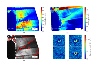
Figure 2a shows the spatial dependence of the AFM (001) reflection at T = 85 K. In contrast to the (002) crystallographic reflection (Fig. 1b), we observe that the A-type AFM is not homogeneous. Rather, two distinct regions are observed, labelled type I and II and denoted in red in Fig. 1c. Domain walls run along the and the directions, but not along . There are three main characteristics of these regions. Firstly, the two regions are not equally populated over the measured crystal volume, with type II occupying approximately two thirds of the investigated volume. Secondly, type II regions exhibit some intriguing fine structure that is absent in type I. Finally, for this orientation of the sample, the intensity of the A-type (001) reflection is much lower in type I than in type II. There are two possible explanations for this. Either the difference in intensity is due to a reduction of the A-type AFM order parameter in type I regions, or there is a different orientation of the ordered moment relative to the incident x-ray beam in the two regions. In order to distinguish between these two scenarios we measured the same area, after rotating the sample around the surface normal. If a diminished order parameter is assumed and all areas have the same direction of the ordered moment, then only a change in the global intensity would be observed. Fig. 2b shows the same area after the rotation. An inversion of the intensity ratio between regions of type I and II is clearly visible. This result indicates that both regions are AFM domains and that the ordered moment forms an angle of approximately 90o between regions I and II. The Cr fiducial mark is parallel to the [100] crystallographic direction. This implies that the ordered moment is parallel to the [100] and [010] direction in regions of type I and II respectively. (Note that there may also exist AFM domains which have the same ordered moment direction but a different phase. Our method does not allow us to discriminate these domains).
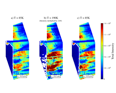
We now turn to the evolution of the A-type AFM domains with temperature. A map at 85 K taken over a large region and at the original orientation, is shown in Fig. 3a. Fig. 3b shows a map taken on warming to 190 K, close to the Néel temperature of 205 K. Comparing Fig. 3a and Fig. 3b we find that the overall intensity of each region has decreased to 36% of the value at 85 K, consistent with the reduction of the global order parameter for these two temperatures Wilkins et al. (2003). The actual domain pattern however, once rescaled by the overall intensity, is indistinguishable between the two cases. We further warmed the sample to 300 K, at which point no signal was observed from any point on the sample. To eliminate possible hysteresis, the sample was then cooled to 12 K and warmed back to 85 K. The map obtained after this thermal cycle is shown in Fig. 3c. The same global intensity was recovered as at 85 K. Surprisingly, we find that the domain pattern was not altered by this thermal cycling; the two measurements are indistinguishable. This demonstrates that both the A-type AFM domain patterns and the spin directions are quenched. We conclude that the overall domain pattern is governed by features intrinsic to the particular crystal and that are not annealed by warming to 300 K. Strain or internal fields could be involved in the appearance of the observed domain pattern, which may not be visible in the measurement of the (002).
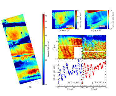
We address now the fine structure observed within the type II domains (Fig. 4a). In order to further characterize these “ripples”, a map with much higher resolution (step size 200 n m ) was measured from a small area of type II (Fig. 4d), Figure 4e shows a periodic modulation with a period of µ m and an intensity modulation of %. A similar analysis at T = 190 K, showed that while the overall intensity has decreased, consistent with the reduced value of the order parameter at this temperature, the ripples are still observed. From the line-out in Fig. 4g the period and amplitude of the ripple modulation is almost identical to that at 85 K. This modulation could be due to a spatial variation of the order parameter (the magnitude of the ordered moment), or of the ordered moment direction. Applying the same experimental method used earlier, we compare images at two different rotations around the surface normal. Comparing Fig. 4b and Fig. 4c we observe that the part of the ripples which are of high intensity at are of low intensity at , while regions of low intensity at , have the same intensity at . Such behavior is only consistent with the intensity modulation arising from the ordered moment direction oscillating between the and directions.
One appealing explanation for this is that the long-period “ripple” structure is caused by the presence of the Dzyaloshinskii-Moriya (DM) interaction arising from the loss of inversion symmetry at each bilayer. It is well known that in multiferroics Khomskii (2009) and even at the metal-vacuum interface Bode et al. (2007); Ferriani et al. (2008) the loss of inversion symmetry often results in the system forming a long period cycloidal-type magnetic structure. In these materials, a cycloidal magnetic structure can induce an electric polarization and vice versa. By analogy with both these cases, the loss of inversion symmetry along the c-axis at each bilayer could lead to a cycloidal component to the magnetic structure, with moments rotating in the b-c plane. The consequences of this within the context of our measurements would be to observe an oscillating moment between the and directions, since the x-ray measurements are only sensitive to the component of the ordered moment along the exit wave vector. The problem in this explanation is the large period of the ripples (4 microns). The longest period known in multiferroic systems is the periodic spin modulation in BiFeO3 of approximately 630 Å, which is almost 100 times shorter than the ripple period observed here. A larger value of dielectric constant would be expected in the present case (La0.96Sr2.04Mn2O7 is close to metallic) which would lead to a sufficiently large increase of the period of the cycloid. This, however, remains an open question.
The experimental data shown here present some interesting facts about the AFM domain structure in La0.96Sr2.04Mn2O7. We have observed the existence of two different A-type AFM regions in the sample. These regions have the same -vector, but ordered moment directions that differ by . The domain walls separating these two regions run along the and directions but not along . Further, the two regions have an unequal population with region II occupying about 70% of the measured volume. When studied in detail, Regions I and II were found not to be symmetry related and therefore are not AF domains in the true sense. For example, we found that type II regions exhibit fine structure, absent in type I. These differences between regions with the ordered moment along and are, a priori, not to be expected from the known La0.96Sr2.04Mn2O7 crystal structure. The observed behavior strongly suggests that the - and -axes are not equivalent and that therefore the system is orthorhombic and regions I and II are better classified as different regions of A-type AFM ordering. We have observed that both the domain pattern and spin direction are quenched and the material exhibits a kind of ‘memory’ which cannot be annealed upon warming to 300 K.
With such a quenched domain structure, we are left wondering what determines the domain pattern? The measurements of the Bragg reflection show that, at least on length scales of n m , the sample is crystallographically homogeneous, that is the intensity of the reflection varies to less than 15% and the position is unchanged within errors. The observed domain pattern and behavior is different to that observed in some other well studied antiferromagnets. In rhombohedral NiO Roth (1960); Slack (1960), while the type of domain walls that separate regions of different magnetic vector, do indeed run along crystallographic directions, the domains are far larger (over several mm in size), and warming above is sufficient to anneal the domain walls Roth (1960). In addition, in NiO the regions of different spin directions in a single magnetic -vector region form a nearly random pattern in zero applied magnetic field Roth (1960). Overall, La0.96Sr2.04Mn2O7 appears to behave rather differently. One possible explanation is that the domain wall positions are governed by the presence of crystallographic or magnetic imperfections locked in during the crystal growth process.
We hope that the present results will stimulate further theoretical and experimental work on the origin of this intriguing domain pattern and the role that these previously inaccessible images of domain structures play in the evolution of the phase diagrams of strongly correlated electron systems, and even new emergent properties.
Acknowledgements.
The authors would like to thank John Hill, Jing Tao and Simon Billinge for stimulating discussions. Technical assistance from William J. Leonhardt, D. Scott Coburn, Sue Wirick and William Schoenig is especially noted. We would also like to acknowledge the support of Xiao Tong with AFM measurements. This research was funded by the Department of Energy, Office of Basic Energy Sciences, under Contract No. DE-AC02-98CH10886 at Brookhaven National Laboratory and DE-AC02-06CH11357 at Argonne National Laboratory. Part of this research was carried out at the Center for Functional Nanomaterials, Brookhaven National Laboratory.References
- Hubert and Schaefer (1998) A. Hubert and R. Schaefer, Magnetic Domains - The Analysis of Magnetic Microstructures (Springer-Verlag, Berlin Heidelberg, New York, 1998).
- Neel (1955) L. Neel, C. R. Acad. Sci. Paris 241, 533 (1955).
- Landau et al. (1984) L. D. Landau, L. P. Pitaevskii, and E. Lifshitz, Electrodynamics of Continuous Media, Second Edition: Volume 8 (Course of Theoretical Physics) (Butterworth-Heinemann, 1984).
- Scholl et al. (2000) A. Scholl, J. Stoehr, J. Luening, J. W. Seo, J. Fompeyrine, H. Siegwart, J.-P. Locquet, F. Nolting, S. Anders, E. E. Fullerton, M. R. Scheinfein, and H. A. Padmore, Science 287, 1014 (2000).
- Nogues et al. (2005) J. Nogues, J. Sort, V. Langlais, V. Skumryev, S. Suriach, J. Muoz, and M. Baro, Physics Reports 422, 65 (2005).
- Park et al. (2011) B. G. Park, J. Wunderlich, X. Marti, V. Holy, Y. Kurosaki, M. Yamada, H. Yamamoto, A. Nishide, J. Hayakawa, H. Takahashi, A. B. Shick, and T. Jungwirth, Nat Mater 10, 347 (2011).
- Tranquada et al. (2008) J. M. Tranquada, G. D. Gu, M. Hücker, Q. Jie, H.-J. Kang, R. Klingeler, Q. Li, N. Tristan, J. S. Wen, G. Y. Xu, Z. J. Xu, J. Zhou, and M. v. Zimmermann, Phys. Rev. B 78, 174529 (2008).
- Mauri et al. (1987) D. Mauri, H. C. Siegmann, P. S. Bagus, and E. Kay, J. Appl. Phys. 62, 3047 (1987).
- Malozemoff (1987) A. P. Malozemoff, Phys. Rev. B 35, 3679 (1987).
- Miltenyi et al. (2000) P. Miltenyi, M. Gierlings, J. Keller, B. Beschoten, G. Guentherodt, U. Nowak, and K. D. Usadel, Phys. Rev. Lett. 84, 4224 (2000).
- Nowak et al. (2002) U. Nowak, K. D. Usadel, J. Keller, P. Miltenyi, B. Beschoten, and G. Guentherodt, Phys. Rev. B 66, 014430 (2002).
- Stoehr et al. (1999) J. Stoehr, J.hr, A. Scholl, T. J. Regan, S. Anders, J. Luening, M. R. Scheinfein, H. A. Padmore, and R. L. White, Phys. Rev. Lett. 83, 1862 (1999).
- Wilkins et al. (2003) S. B. Wilkins, P. D. Hatton, M. D. Roper, D. Prabhakaran, and A. T. Boothroyd, Phys. Rev. Lett. 90, 187201 (2003).
- Abbamonte et al. (2004) P. Abbamonte, G. Blumberg, A. Rusydi, A. Gozar, P. G. Evans, T. Siegrist, L. Venema, H. Eisaki, E. D. Isaacs, and G. A. Sawatzky, Nature 431, 1078 (2004).
- Garcia-Fernandez et al. (2009) M. Garcia-Fernandez, U. Staub, Y. Bodenthin, V. Scagnoli, V. Pomjakushin, S. W. Lovesey, A. Mirone, J. Herrero-Martin, C. Piamonteze, and E. Pomjakushina, Physical Review Letters 103, 097205 (2009).
- Kim et al. (2005) J. W. Kim, A. Kreyssig, L. Tan, D. Wermeille, S. L. Bud’ko, P. C. Canfield, and A. I. Goldman, Applied Physics Letters 87, 202505 (2005).
- Hiraoka et al. (2011) Y. Hiraoka, Y. Tanaka, T. Kojima, Y. Takata, M. Oura, Y. Senba, H. Ohashi, Y. Wakabayashi, S. Shin, and T. Kimura, Phys. Rev. B 84, 064418 (2011).
- Hatzakis et al. (1980) M. Hatzakis, B. J. Canavello, and J. M. Shaw, IBM J. Res. Dev. 24, 452 (1980).
- Hill and McMorrow (1996) J. P. Hill and D. F. McMorrow, Acta Crystallographica Section A 52, 236 (1996).
- Khomskii (2009) D. Khomskii, Physics 2, 20 (2009).
- Bode et al. (2007) M. Bode, M. Heide, K. von Bergmann, P. Ferriani, S. Heinze, G. Bihlmayer, A. Kubetzka, O. Pietzsch, S. Blugel, and R. Wiesendanger, Nature 447, 190 (2007).
- Ferriani et al. (2008) P. Ferriani, K. von Bergmann, E. Y. Vedmedenko, S. Heinze, M. Bode, M. Heide, G. Bihlmayer, S. Bluegel, and R. Wiesendanger, Phys. Rev. Lett. 101, 027201 (2008).
- Roth (1960) W. Roth, J. Appl. Phys. 31, 2000 (1960).
- Slack (1960) G. Slack, J. Appl. Phys. 31, 1571 (1960).