Quantized coexisting electrons and holes in graphene measured using temperature dependent magneto-transport
Abstract
We present temperature-dependent magneto-transport experiments around the charge neutrality point in graphene and determine the amplitude of potential fluctuations responsible for the formation of electron-hole puddles. The experimental value meV is considerably larger than in conventional semiconductors which implies a strong localization of charge carriers observable up to room temperature. Surprisingly, in the quantized regime, the Hall resistivity overshoots the highest plateau values at high temperatures. We demonstrate by model calculations that such a peculiar behavior is expected in any system with coexisting electrons and holes when the energy spectrum is quantized and the carriers are partially localized.
pacs:
72.80.Vp, 73.43.-f, 73.63.-b, 71.70.DiI Introduction
Pristine graphene is a zero-gap semiconductor where the conduction and valence band touch at zero energy. This point is generally referred to as the charge neutrality point (CNP) with a zero charge carrier density. However, it has been shown experimentally, that for graphene on Si/SiO2 substrates, electrons and holes coexist around the CNP, which is attributed to the presence of spatially inhomogeneous conducting electron-hole puddles.Tan et al. (2007); Zhang et al. (2009); Martin et al. (2008); Rutter et al. (2011)
In this paper we investigate the coexistence of electrons and holes by means of temperature-dependent magneto-transport around the CNP. We present results in the classical and quantum-Hall regimes. In the classical regime, the individual charge carrier concentration and conductivity at the CNP increases with increasing temperature due to thermal activation but, as a consequence of potential fluctuations, do not vanish even at the lowest temperature. From this temperature dependence, we determine the strength of the potential fluctuations responsible for the formation of electron-hole puddles, meV for our samples. In the quantum Hall regime, the Hall resistance shows higher values than expected suggesting a deactivation of charge carriers with increasing temperature. Using model calculations, however, we demonstrate that this counterintuitive temperature dependence is straightforwardly explained considering the quantized density of states of coexisting electrons and holes.
The paper is organized as follows: In Sec. II we shortly describe the samples an measurements. Sec. III is devoted to the experiential magneto-transport in the classical regime along with an interpretation of the results. In Sec. IV we describe experimentally (subsection IVA) and discuss theoretically (subsection IVB) magneto-transport data in the quantum-Hall regime. The paper ends with a conclusion in Sec. V
II Experimental
We have measured two field effect transistors made from single layer graphene (SLG) and bilayer graphene (BLG) deposited on Si/SiO2 wafers and shaped into a 1m wide Hall bar. Both flakes originate from natural graphite and have mobilities m-2 s-1 and m-2 s-1, respectively. The total charge carrier concentration is controlled by applying a gate voltage on the conducting Si substrate:Novoselov et al. (2004)
| (1) |
with m-2/V for a 300 nm thick SiO2 gate insulator. The subscripts and indicate electrons and holes, respectively.
Magneto-transport as a function of magnetic field, carrier concentration and temperature were performed in a temperature range between 0.5 K and 250 K using a top-loading He-3 system and a variable-temperature insert in a 33 T Bitter magnet.
III Classical Regime
Fig. 1(a) shows for the BLG sample at T for different temperatures. Down to the lowest temperatures, the Hall resistivity does not exhibit quantized plateaus at this magnetic field, indicating a continuous energy spectrum. For all temperatures, the Hall resistance smoothly crosses zero at the CNP, which indicates that electrons and holes are present at all gate voltages.Wiedmann et al. (2011)
In this coexistence regime, the simultaneous contribution of electrons and holes with equal mobility to the Hall effect is given by:Ashcroft and Mermin (1976); Hwang et al. (2007)
| (2) |
Note that this expression originally derived for massive charge carries with mobility ( is the elastic scattering time and is the effective mass) is also valid for massless particles when defining the mobility more generally as the ratio between the average drift velocity of the carriers and the applied electric field.
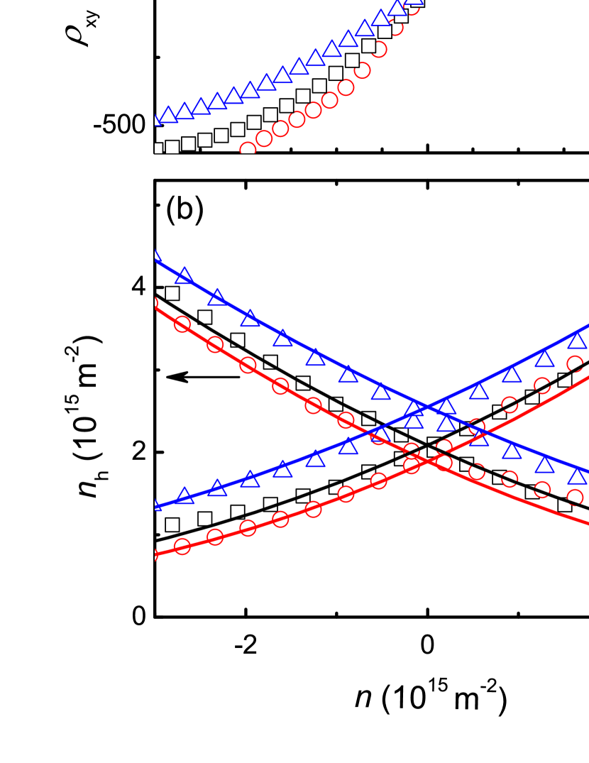
By solving the system of Eqs. (1) and (2) with respect to the variables and for each point of the experimental dependence, we can determine the number of electrons and holes independently,Wiedmann et al. (2011) the results are shown in Fig. 1(b).
At the CNP () and are equal to a residual concentration , which is, according to Eq. 2, related to the slope of at the CNP:
| (3) |
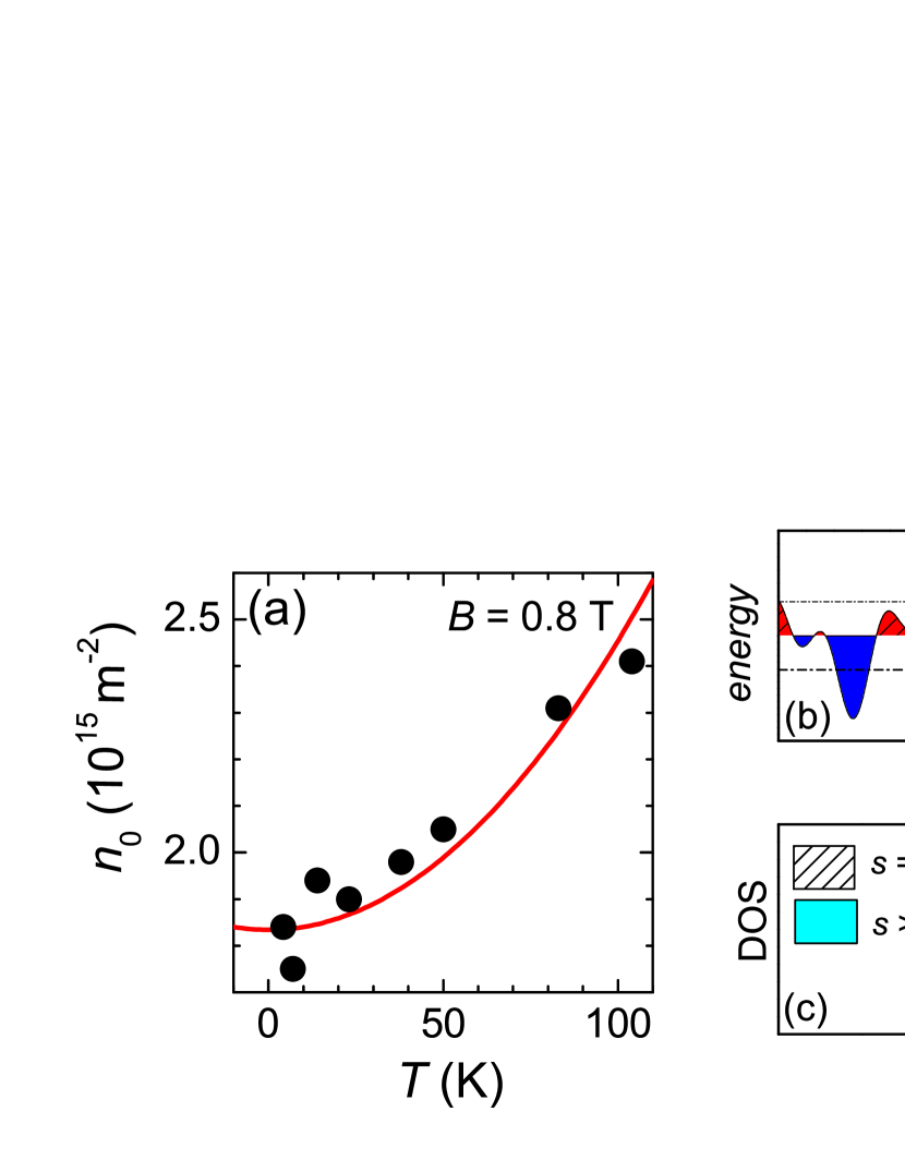
(b) Sketch of the random potential fluctuations in the sample yielding a broadened effective density of states shown in (c).Hwang and Das Sarma (2010)
The temperature dependence of is plotted in Fig. 2(a). At zero temperature we find that a finite number of both electrons and holes are present at the CNP. These electron-hole puddles originate from spatial potential fluctuations within the sample represented schematically in Fig. 2(b) and lead to an effective density of states (DOS) around the CNP plotted in Fig. 2(c):Hwang and Das Sarma (2010)
| (4) |
is the amplitude of potential fluctuations.
Though the question whether the puddles are caused by the impurity potential alone or by intrinsic ripples in graphene is still under discussion,Gibertini et al. (2012) this phenomenological DOS is not sensitive to the deeper origin of the puddles. The calculated charge carrier concentrations using this effective DOS, shown by the solid lines in Fig. 1(b), indeed reproduce the experimentally observed behavior around the CNP.
Directly at the CNP, the temperature dependence in a low temperature () approximation is analytically found to be:Hwang and Das Sarma (2010)
| (5) |
Analogously, the temperature dependence of the conductivity at the CNP can be described by:Hwang and Das Sarma (2010)
| (6) |
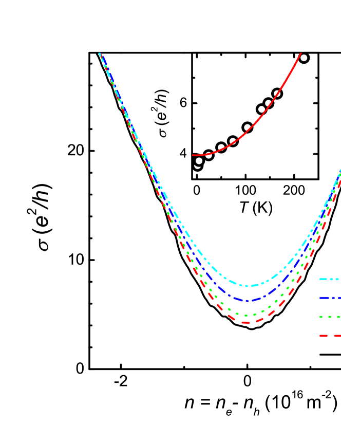
The fit of the experimental temperature dependence in the classical regime with Eq. (6) is shown in the inset Fig. 3 for the 0 T trace. The fit yields meV, which is close to the value meV, determined from the fit to the Hall data.
Remarkably, this strength of potential fluctuations is comparable to the thermal energy at room temperature and considerably larger than in conventional semiconductor heterostructures.Nixon and Davis (1990) Therefore, whereas quantum Hall localization in GaAs-based systems breaks down above 30 K,Rigal et al. (1999) the strong potential fluctuations can induce a robust localization of charge carriers in graphene when the Fermi energy is situated between two Landau levels, in particular around filling factor .Giesbers et al. (2007) This allows the QHE to persist up to room-temperature.Novoselov et al. (2007); Rem
IV Quantized Regime
IV.1 Experimental Results
Fig. 4(a) shows the measured Hall effect for BLG as a function of the total charge carrier concentration at T for various temperatures. For T the system is in the quantized regime and we observe plateaus at as expected for BLG. At the lowest temperatures, also a plateau develops at which makes the curve slightly asymmetric. However, since the plateau is smoothed out for K, we neglect this asymmetry in the following.
At K, the Hall resistance on the electron (hole) side reaches its maximum (minimum) value at the plateau and goes smoothly to the hole (electron) side as already observed in the non-quantized regime and this behavior can again be qualitatively explained by the two-carrier model. At high temperatures, the Hall resistivity overshoots the plateau before the beginning of the plateau and reaches values higher than and becomes steeper at the CNP, see Fig. 4(a). We observe a similar behavior in the SLG sample, therefore, this effect has a generic nature and was also observed by others.Jiang et al. (2007a) Note that these overshoots in the Hall resistance only appears at high temperatures and is therefore not due to the (partial) splitting of the lowest Landau level as observed in e.g. Ref. Jiang et al., 2007b.
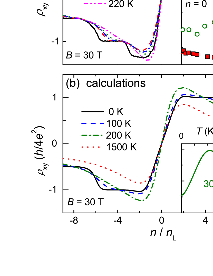
The temperature dependence of the slope of at the CNP is explicitly shown in the inset to Fig. 4(a). It is opposite to the classical regime, which can be seen by comparison of the traces at T (quantized regime) and T (classical regime), plotted together in the inset.
According to Eq. (3), an increase in the slope with increasing temperature corresponds to a decrease of the charge carrier concentration, which appears to be counter-intuitive. However, the plateaus remain visible up to the highest temperature measured, i.e., the system remains quantized and the number of electrons and holes within one Landau level is fixed. In the quantized regime, the slope of the Hall resistivity depends not only on the number of charge carriers at the CNP, but also the strength of localization, i.e. the width of the plateaus closest to the CNP. Therefore, Eq. (3) cannot be used to relate the slope to the number of charge carriers. In fact, Eq. (2), which predicts a -behavior of the slope around the CNP when , anticipates such an overshoot.
A similarly unexpected behavior for high temperature is observed in the resistance at high magnetic fields. Fig. 4(c) shows the resistivity of BLG in the quantized regime as a function of the total charge carrier concentration for various temperatures. In contrast to the non-quantized regime, the resistivity exhibits a metal-like increase with temperature.
As we will show in the following subsection, this peculiar transport properties in the quantized regime can be described in a simple DOS model with localized and extended states where the temperature dependence of the resistivity is governed by a redistribution of charge carriers due to the thermal activation.
IV.2 Model Calculations and Discussion
The model used for our calculation starts with the quantized DOS for graphene in magnetic field consists of separate Gaussian-shaped Landau levels (LLs) as depicted schematically in Fig. 5. States in the middle of each LL are extended, and states are localized in the tails. For our simulations of the DOS in BLG shown below, we have used a constant width K for the higher Landau levels and K for the zero-energy LL.Kurganova et al. (2010) Landau levels above (below) the CNP, populated by electrons (holes), have a degeneracy of . The zeroth LL with a degeneracy of for SLG and for BLG is populated by electrons and holes simultaneously, such that electron and hole conduction can be found both above and below the CNP. We can then calculate the conductivity, using the Kubo-Greenwood formalism,Kubo (1956); Greenwood (1958):
Here is the Fermi distribution and is an energy dependent function containing the density of the extended states, the particle velocity and the scattering time. the upper indices correspond to electrons and holes, respectively. Modeling by a superposition of Gaussians with the above mentioned widths, the Kubo-Greenwood formula reproduces qualitatively the behavior of the experimental conductivity in graphene, but does not give a universal value of minimal conductivity.Ziegler (2007) Therefore, we normalized the integral in Eq. (IV.2) such that, at zero temperature, at the CNP has the universal value of in accordance with the experimentally observed value.
Similarly, we can determine the Hall conductivity by summing up all extended states below the Fermi level, smeared out by temperature:
| (8) |
When introducing a localized DOS, the calculated conductivity develops plateaus which are not at multiples of ,von Klitzing (1985) because the number of extended states within a LL is less than the total level degeneracy. In order to reproduce the correct number of occupied LLs in Eq. (8), we have normalized the extended DOS for each LL to the total number of extended states within it.
After calculating the conductivities we convert them into the resistivity and the Hall resistivity using the standard matrix relations, the results are shown in Fig. 4(b) and (d). They can be compared to the experimental curves, plotted as panels (a) and (c) of the figures. The calculated curves reproduce qualitatively the experimental results, and display a similar temperature dependence. In particular, at the CNP, the resistivity (insets in Fig. 4(c) and (d)) and the slope of the Hall resistivity (insets in Fig. 4 (a) and (b)) increase with increasing temperature up to 200 K. Moreover, as is also seen in the experiment, the overshoots develop at the beginning of the plateaus at high temperatures (compare panels (a) and (b) in Fig. 4).
Starting from about 500 K (as calculated for 30 T) the system smoothly enters the classical regime. The conductivity (inset to Fig. 4(d)) starts to increase with increasing temperature and the slope of the Hall resistivity (inset to Fig. 4(b)) decreases. Experimentally, this trend in the non-quantized regime is verified by the low field data presented earlier in Figs. 2 and 3.
V Conclusions
To conclude, we have investigated the coexistence of electron and hole magneto-transport in graphene for a wide range of temperatures and magnetic fields. For all temperatures and fields, the Hall resistivity smoothly crosses zero at the CNP indicating the simultaneous presence of both electrons and holes at the CNP. In the non-quantized regime, the slope of the Hall resistivity decreases with increasing temperature, which is accompanied by an increasing conductivity at the CNP. This behavior can be quantitatively modeled by a thermal activation of charge carriers experiencing relatively large potential fluctuation of the order of 20 meV.
In the quantum Hall regime, increasing the temperature has the opposite effect on the slope of the Hall effect and produces counter-intuitive overshoots when approaching the plateaus. Using an appropriate density of states, we have shown in model calculations that such a behavior is expected for any two-carrier system with a quantized energy spectrum.
VI Acknowledgments
Part of this work has been supported by EuroMagNET under EU contract RII3-CT-2004-506239 and by the Stichting Fundamenteel Onderzoek der Materie (FOM) with financial support from the Nederlandse Organisatie voor Wetenschappelijk Onderzoek (NWO).
References
- Tan et al. (2007) Y.-W. Tan, Y. Zhang, K. Bolotin, Y. Zhao, S. Adam, E. H. Hwang, S. Das Sarma, H. L. Stormer, and P. Kim, Phys. Rev. Lett. 99, 246803 (2007).
- Zhang et al. (2009) Y. Zhang, V. W. Brar, C. Girit, Z. A., and M. F. Crommie, Nature Physics 5, 722 (2009).
- Martin et al. (2008) J. Martin, N. Akerman, G. Ulbricht, T. Lohmann, J. H. Smet, K. von Klitzing, and A. Yacoby, Nature Physics 4, 144 (2008).
- Rutter et al. (2011) G. M. Rutter, S. Jung, N. N. Klimov, D. B. Newell, N. B. Zhitenev, and J. A. Stroscio, Nature physics 7, 649 (2011).
- Novoselov et al. (2004) K. S. Novoselov, A. K. Geim, S. V. Morozov, D. Jiang, Y. Zhang, S. V. Dubonos, I. V. Grigorieva, and A. A. Firsov, Science 306, 666 (2004).
- Wiedmann et al. (2011) S. Wiedmann, H. J. van Elferen, E. V. Kurganova, M. I. Katsnelson, A. J. M. Giesbers, A. Veligura, B. J. van Wees, R. V. Gorbachev, K. S. Novoselov, J. C. Maan, and U. Zeitler, Phys. Rev. B 84, 115314 (2011).
- Ashcroft and Mermin (1976) N. W. Ashcroft and N. D. Mermin, Solid State Physics (Saunders College Publishing, p.240, 1976) p. p.240.
- Hwang et al. (2007) E. H. Hwang, S. Adam, and S. Das Sarma, Phys. Rev. B 76, 195421 (2007).
- Hwang and Das Sarma (2010) E. H. Hwang and S. Das Sarma, Phys. Rev. B 82, 081409 (2010).
- Gibertini et al. (2012) M. Gibertini, A. Tomadin, F. Guinea, M. I. Katsnelson, and M. Polini, Phys. Rev. B 85, 201405 (2012).
- Nixon and Davis (1990) J. A. Nixon and J. H. Davis, Phys. Rev. B 41, 7929 (1990).
- Rigal et al. (1999) L. B. Rigal, D. K. Maude, M. Potemski, J. C. Portal, L. Eaves, Z. R. Wasilewski, G. Hill, and M. A. Pate, Phys. Rev. Lett. 82, 1249 (1999).
- Giesbers et al. (2007) A. J. M. Giesbers, U. Zeitler, M. I. Katsnelson, L. A. Ponomarenko, T. M. Mohiuddin, and J. C. Maan, Phys. Rev. Lett. 99, 206803 (2007).
- Novoselov et al. (2007) K. S. Novoselov, Z. Jiang, Y. Zhang, S. V. Morozov, H. L. Stormer, U. Zeitler, J. C. Maan, G. S. Boebinger, P. Kim, and A. K. Geim, Science 315, 1379 (2007).
- (15) The recent observation of a robust quantum Hall effect in InSb systems (Ref. Alexander-Webber et al., 2012) may indicate that such a robust localization can also be achieved in conventional semiconductor heterojunctions.
- Jiang et al. (2007a) Z. Jiang, Y. Zhang, Y.-W. Tan, H. Stormer, and P. Kim, Solid State Commun. 143, 14 (2007a).
- Jiang et al. (2007b) Z. Jiang, Y. Zhang, H. L. Stormer, and P. Kim, Phys. Rev. Lett. 99, 106802 (2007b).
- Kurganova et al. (2010) E. V. Kurganova, A. J. M. Giesbers, R. V. Gorbachev, A. K. Geim, K. S. Novoselov, J. C. Maan, and U. Zeitler, Solid State Commun. 150, 2209 (2010).
- Kubo (1956) R. Kubo, Canad. J. Phys. 34, 1274 (1956).
- Greenwood (1958) D. A. Greenwood, Proc. Phys. Soc. London 71, 585 (1958).
- Ziegler (2007) K. Ziegler, Phys. Rev. B 75, 233407 (2007).
- von Klitzing (1985) K. von Klitzing, Rev. Mod. Phys. 58, 519 (1985).
- Alexander-Webber et al. (2012) J. A. Alexander-Webber, A. M. R. Baker, P. D. Buckle, T. Ashley, and R. J. Nicholas, Phys. Rev. B 86, 045404 (2012).