In situ visualization of Ni-Nb bulk metallic glasses phase transition.
Abstract
We report the results of in situ investigation of the Ni-based bulk metallic glass structural evolution and crystallization behavior. The X-ray diffraction (XRD), transmission electron microscopy (TEM), nano-beam diffraction (NBD), differential scanning calorimetry (DSC), radial distribution function (RDF) and scanning probe microscopy/spectroscopy (STM/STS) techniques were applied to analyze the structure and electronic properties of glasses before and after crystallization. It was proved that partial surface crystallization of can occur at the temperature lower than that for the full sample crystallization. According to our STM measurements the primary crystallization originally starts with the phase formation as a leading eutectic phase. It was shown that surface crystallization drastically differs from the bulk crystallization due to the possible surface reconstruction. The mechanism of glass alloy 2D-crystallization was suggested, which corresponds to the local metastable surface phase formation. The possibility of different surface nano-structures development by the annealing of the originally glassy alloy in ultra high vacuum at the temperature lower, than the crystallization temperature was shown. The increase of the mean square surface roughness parameter while moving from glassy to fully crystallized state can be caused by concurrent growth of and bulk phases. The simple empirical model for the estimation of cluster size was suggested, and the obtained value (about 8 Å) is in good agreement with the STM measurements data (8 Å-10 Å).
keywords:
bulk metallic glasses , STM , phase transitionPACS:
64.70.pe , 68.37.Ef , 68.37.LpActa Materialia \runauth \jidprocs \jnltitlelogoActa Materialia \CopyrightLine2011Published by Elsevier Ltd.
1 Introduction
Amorphous metallic glasses were segregated in a separate class of materials starting from classic rapid-solidification experiments on Au–Si alloys performed by Duwez and colleagues [1]. Later a new class of metallic glasses called bulk metallic glasses with high glass-forming ability were invented [2, 3]. Metallic glasses (especially bulk metallic glasses) currently attract a significant attention of the scientists involved in the materials science research [2, 3, 4, 5, 6, 7]. In these works the unique mechanical (high strength and large elastic deformation limit), chemical (high corrosion resistance) and magnetic properties (either extremely soft or moderately hard magnetism) were intensively studied. The physical and chemical properties of metallic alloys in an amorphous state significantly differ from the properties of metallic alloys in a crystalline state. The strength and hardness values of the amorphous alloys exceed that of the crystals one, due to “disordered“ local structure of metallic glasses, while the elastic modulus of normal elasticity is slightly lower than in the crystalline state. An elastic modulus difference can be caused by the more loosely packed structure of metallic glasses due to the smaller number of the nearest neighbors in the atomic structure. Therefore the creation of partially crystallized structures can open new outlooks for metallic glasses properties improvement [8].
Until now the majority of the investigations dedicated to metallic glasses study were oriented on the obtaining of the information about local arrangement of the constituted components. Transmission electron microscope and diffraction methods were mainly applied for these purposes [9]. Spectroscopic information was obtained from photoemission experiments [10]. But a detailed information on a subnanometer scale is required for full understanding of processes which take place during metallic glasses phase transition from the amorphous state to crystalline one. Scanning tunneling microscopy/spectroscopy (STM/STS) [11, 12] is a very powerful method for getting the necessary information, but only a few works [13, 14, 15] were devoted to STM/STS study of bulk metallic glasses surface. In [15] scanning tunneling microscopy was applied to investigate time evolution of the metallic glassy surface with temporal resolution as fast as 1 minute per scan and extending up to 1000 minutes. It was shown that rearrangements of surface clusters occur almost exclusively by two-state hopping. In [13] UHV STM/STS measurements of bulk metallic glasses surface topography and electronic properties at the room temperature were performed. The pseudo-gap at Fermi energy and linear part of the normalized tunneling conductivity spectra were revealed in consistence with suggested theoretical model. It was shown that the additional features on the averaged normalized tunneling conductivity are connected with the presence of localized states in individual clusters on the surface. The theoretical analysis of electron elastic scattering on the impurities inside each cluster and on the random defects on the cluster boundaries in the presence of intra-cluster Coulomb interaction of the scattering electrons has been applied to explain the experimental results. In [14] we investigated the processes of bulk metallic glasses crystallization by means of STM. We pointed out the existence of three different surface lattice structures observed during full crystallization that are completely different from those formed according to Ni-Nb binary phase diagram in the bulk sample.
In this work we present the results of the comprehensive investigation of the Ni-based bulk metallic glass structural evolution and crystallization behavior by X-ray diffraction (XRD), including radial distribution function (RDF) analysis, transmission electron microscopy (TEM), nano-beam diffraction (NBD), differential scanning calorimetry (DSC) and scanning probe microscopy/spectroscopy (STM/STS) methods.
2 Experimental procedure
An ingot of the alloy (composition is given in nominal atomic percentage) was prepared by arc-melting mixtures of Ni (99.99 mass.% purity) and Nb (99.9 mass.% purity) under an argon atmosphere. From this ingot, bulk rod sample of 1 mm in diameter was prepared by the injection casting technique in an argon atmosphere from the initial arc-melted ingot. The structure of the cast samples was examined by conventional X-ray diffractometry (XRD).
The samples were cut along the rod axis before loading to the STM holder. The surface suitable for STM/STS study was obtained by grinding process with further treatment of the surface using polishing slurry with particle sizes of 5, 1, and 0.5 to get flat and mirror like surface. The quality of prepared surface was controlled by optical microscope with 800 nm resolution. Before placing the samples in STM holder they were ultrasonically cleaned in acetone and distilled water. Samples were degassed at 673 K during 24 hours and processed with argon-ion-sputtering (1.5 keV, 30 A, 60 min) at torr argon pressure. At the final stage of clean surface preparation the samples were heated again starting from 673 K (to get clean surface in amorphous state) (which is 257 K below its crystallization temperature equal to 930 K [16]) and higher (up to 973 K) during 12 hours at torr pressure range.
All STM/STS experiments were performed using commercial UHV Omicron system with base pressure torr at room temperature. In our experiments we used tungsten tips obtained by electrochemical etching. To remove the oxide layer from the STM tip apex, they were annealed at 1473 K at ultra high vacuum conditions (less then torr). Bias voltage was applied to the sample, while STM tip was virtually ground. The current imaging tunneling spectroscopy (CITS) curves were obtained simultaneously with constant current images. The STM images were 400400 points in size, while the CITS images were 8080 points. The I(V) spectrum was taken at each fifth point of each fifth line of the scanning frame.
Transmission electron microscopy (TEM) investigations were carried out using a JEOL JEM 2010 microscope operating at 200 keV. The samples for TEM were prepared mechanically (down to 10 thickness) and by subsequent ion polishing (down to electron-beam transparency). In order to avoid structural damage the ion-beam energy was kept as low as 2.0 keV. Nanobeam diffraction (NBD) patterns were also obtained in the transmission electron microscope.
Synchrotron radiation x-ray diffraction measurements were carried out using a high energy monochromatic beam at ID11 beam line of the European Synchrotron Radiation Facility (ESRF) equipped with a nitrogen cooled double-silicon monochromator. The photon energy was 94 keV. After correction for air scattering, polarization, absorption [17], and Compton scattering [18], the measured intensity was converted to electron units per atom with the generalized Krogh–Moe–Norman method [19], using the x-ray atomic scattering factors and anomalous dispersion corrections [20]. The total structure factor S(Q) (Q-scattering vector) and the interference function Qi(Q) were obtained from the coherent scattering intensity by using atomic scattering factors [21]. The values of Qi(Q) less than 18 were smoothly extrapolated to Q = 0. The radial distribution (RDF(r)) and pair distribution (PDF(r)) functions were obtained by the Fourier transformation of Qi(Q).
3 Results and discussion
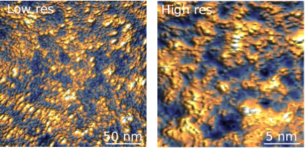
Fig.1 demonstrates typical STM images of the metallic glass surface in the amorphous state. The procedure of surface preparation was described in the previous section. After ion bombardment the sample was heated up to 673 K. The high resolution STM (Fig. 1b) image shows surface structure consisting of 8–10 Å size clusters. Small clusters on a surface have a tendency to coalesce forming the clusters with typical size of about 50 Å [13] (Fig. 1a). We were not able to observe any ordered structure in STM or HRTEM images. The obtained results demonstrate the absence of long-range order on the surface. We suppose that the sample surface can be treated as a disordered structure formed by set of random clusters.
To get information about short-range and medium-range ordering we derived the radial distribution function (Fig. 2) from a synchrotron XRD spectrum. The efficient cluster packing (ECP) model [22, 23, 24] was used to estimate the location and intensity of the RDF peaks, giving a more direct structural interpretation. Both fcc and hcp cluster packing give essentially equivalent peaks and intensities, fcc cluster packing is used for the predictions here. Contact between like atoms is unavoidable in this solute-rich glass, and so the nearest neighbor (NN, or 1st) peak includes both Ni-Ni and Nb-Nb contributions, shown as P1 and P2 respectively in the inset in Figure 2. The partial coordination numbers are estimated from the ECP model [25] to be , so that the dominant contribution to the NN peak comes from Nb-Ni contacts, also shown in Figure 2.
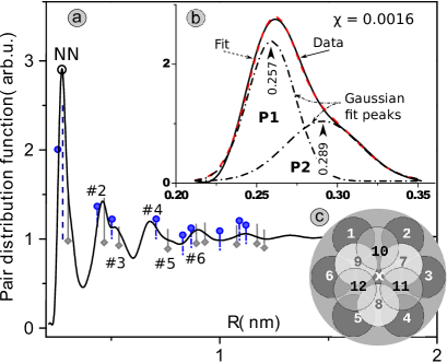
The inset (b) shows deconvolution of the first peak into Ni-Ni and Nb-Nb components. Peak locations and intensities predicted from the efficient cluster packing model are shown for Ni-Ni and Nb-Nb separations. The predicted location and intensity of the Nb-Ni 1st neighbor peak is also shown.
(c) Schematic model of individual cluster observed on surface in the amorphous state. Atoms 10, 11, 12 are located in the upper layer, x, 1, 2, 3, 4, 5, 6 in the middle layer and 7, 8, 9 in the bottom layer. The distance between the atom ”x” and any neighbor atoms (1–12) is 2.57 Å. The outer surround corresponds to the average size of cluster observed in STM experiments.
The location and intensities of the 2nd and 3rd peaks at about 4.6 Å and 5.2 Å are well-predicted, and represent the spacings between clusters that overlap in the 1st coordination shells. The 2nd and 3rd peaks represent atoms on the and sites of the ECP model, respectively. Peaks #4 and #5 at roughly 6.8 Å and 7.7 Å represent the closest contact between non-overlapping clusters along directions of the cluster unit cell. The difference between these two peaks occurs from the difference between Ni-Ni separations (#4) and Nb-Nb separations (#5). Peak #6 is the next-nearest separation between non-overlapping clusters and occurs along directions of the cluster unit cell. The ECP model does not allow estimation of Nb-Ni separations beyond nearest neighbor contact, but the agreement between prediction and experiment is still reasonably good out to distances of about 1 nm.
The position of the first peak () (inset in the Fig. 2) allows us to estimate the nearest neighbor distance (2.57 Å in our case). To our opinion, the distances between Ni and Nb atoms ( Å) and between two nearest Ni atoms ( Å) can contribute to the first peak. The second peak () is located at 2.89 Å and can be responsible for the distance between two nearest Nb atoms ( Å). The area of the first maximum gives evidence of the nearest neighbors number or coordination number ”Z”. We can conclude that in our case the coordination number is equal to 12.47, taking the integral over the RDF(R) curve in the range of values giving contribution for the first peak from 0.22 to 0.35 nm (this means that the surface contains the equal number of clusters with 12 nearest neighbors (13 atoms)). Fig. 2 demonstrates a model of one cluster consisting of 13 atoms (atom, marked by ”x”, has 12 neighbors). The distance between atom ”x” and any of neighbor atoms is 2.57 Å. In our model we used the values of 1.25 Å and 1.47 Å for the radii of Ni and Nb atoms correspondingly (Goldschmidt metallic radii) [26]. In such a way one can estimate the minimum cluster size (all of the cluster atoms are Ni atoms) and the maximum size (all of the cluster atoms are Nb atoms). The obtained values (7.64 Å and 8.08 Å) are in the good agreement with STM measurements (8–10 Å).
Here we have to note that this is just an estimation. More accurate approximation can be reached with DFT modeling. Anyway, spatial size estimation error should be relatively small due to the fact that local electronic density of states distribution for metal can be treated as simple superposition of metallic radii spheres.
To analyze the initial phase of metallic glass crystallization the samples were annealed step by step starting from 883 K, which is still lower than the crystallization temperature (955 K at 40 K/min.) up to 973 K. The surface crystallization starts to appear even at lowest temperature of 883 K (Fig. 3a), i.e. at temperature noticeably lower than the bulk eutectic one [27]. This phenomenon can be connected with the surface-induced crystallization [28].
The melting point of Ni (1726 K) is almost two times smaller than the melting point of Nb (2741 K). If a metallic glass has the local volumes enriched by Ni, the Ni atoms can gain additional mobility in these areas at the temperatures significantly lower than crystallization temperature. At 900 K the Nb self-diffusion coefficient is seven times lower than that for Ni [26]. In this case the formation of nano-crystallites from one of amorphous glass components is possible (Ni nano-crystals, for example). The increase of both the annealing time and the temperature leads to the local formation of eutectic phases ( and in our case). We suppose that and phases are growing concurrently. Atomic planes of a few atomic layers thick coming out at the surface (Fig. 3b) most probably represent eutectic structure, composed of the phases including a different Ni content.
The crystallization of the bulk metallic glass was also studied by TEM. Dark-field and bright-field images of the sample annealed at 973 K are shown in Fig. 4(a, b) correspondingly. Nano-structured eutectic is visible in Fig. 4. The results obtained from Nano-Beam Diffraction (NBD) measurements clearly demonstrate an existence of both mentioned above and phases in the bulk of our sample (Fig. 4 (c,d)).
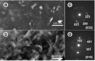
Figure 5 demonstrates XRD pattern of the initial crystallization of metallic glass sample. There are several well distinguishable peaks visible on the diagram corresponding to and phases marked as rectangles and circles correspondingly.
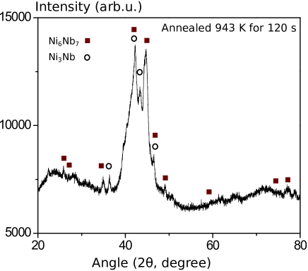
Figure 6 shows the DSC curve of alloy. The alloy exhibits an endothermic like event, characterized by a glass transition temperature . This temperature is a starting point for the amorphous phase-liquid transition. From the temperature the eutectic transformation starts. The second maximum is likely responsible for the growth of eutectic phases.
Here we must note that all of the applied methods: TEM, NBD, XRD and DSC are very useful for the analysis of amorphous alloys initial crystallization but the information extracted from these experiments mainly regards to the bulk properties. Even TEM can be characterized as a bulk method despite of small samples thickness. Besides it is a diffraction method, producing a picture in the reciprocal space. The processes taking place at amorphous alloys surface during initial crystallization can differ radically from the bulk ones.

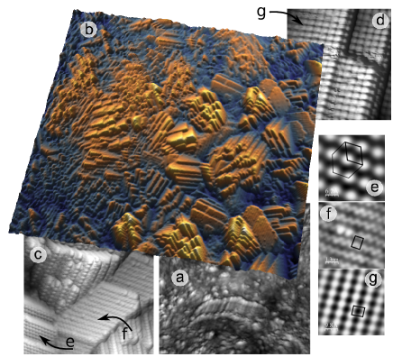
Another interesting point is the origin of the crystallization phenomenon. Does the crystallization process starts to develop from the surface to bulk or vice versa? To get the answers for this question the STM/STS measurements were performed. The undeniable advantage of STM method is a very high spatial resolution. The results of STM investigations are presented in Figure 3. Fig. 3b shows the STM image of the sample annealed at 973 K. The STM image has the size which approximately corresponds to the size of nano-crystal, embedded in the amorphous matrix (bright spot in Fig. 4b), and consists of many randomly oriented facets. The angular distribution for plane inclinations reveals that the angle for the most often observed facets appears in the range 2–12∘. Here is the angle between the normal vectors to facet and to horizontal plane, this means that = 0 for horizontal facets and it increases with the slope.
Fig. 3 c, d demonstrates a part of area presented in Fig. 3b with higher resolution. The analysis of the facets structure reveals the presence of three different surface reconstructions: hexagonal, rectangular and zigzag (Fig. 3 (e, f, g). It is possible to observe three surface structures on different image areas marked by the corresponding arrows. STM image in Fig. 3e shows well defined hexagonal structure with rhomb-shaped unit cell with sizes 7.6Å 7.6Å (marked by black lines in Fig. 3e). Figure 3f demonstrates zigzag surface structure which takes place in the area indicated by arrows f in Fig. 3c. The rectangle shows the primitive unit cell with sizes 7.9Å 10.3Å. Fig. 3g is the high-resolution STM image of rectangular surface structure observed in the area indicated by arrow g in Fig. 3d. The determined parameters of the unit cell are 8.4Å 7.6Å. This one is identical to the structure observed in our experiments with the partially crystallized metallic glass (Fig. 3a). Most probably it corresponds to the orthorhombic crystal system class due to the same symmetry of unit cell.
All the STM images were obtained at negative bias voltage (in filled states bias range). No one of the surface structures corresponds to possible periodicity of monocrystal, monocrystal or , crystals. Because of tunneling spectra similarity we suggest that the rectangular and zigzag structures observed in our STM/STS experiments are two possible surface reconstructions of the phase [14]. The best correspondence was found for hexagonal structure and metastable surface reconstruction . It is well known that the free-electron-like surface states, the Shockley surface states (SS), are present on the Ni(111) surface [29, 30, 31]. If the observed in our experiments hexagonal surface structure (Fig. 3e) corresponds to surface reconstruction , then the Shockley surface states should be visible in our scanning tunneling spectra.
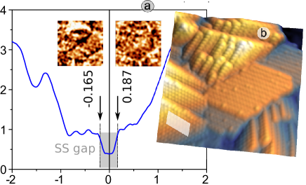
To verify this statement the current imaging tunneling spectroscopy (CITS) measurements were performed. Fig. 7b is the constant current tunneling image. CITS images inside the Fig. 7a were measured at -0.17 V and 0.19 V correspondingly. They represent the same area of the surface as constant current STM image in Fig. 7b with lower resolution ( points). Averaged normalized tunneling conductivity spectrum is presented in Fig. 7a. The averaging was performed within the area, containing rectangular surface structure shown in Fig. 7b.
It was demonstrated in [14] that the position of the peaks in the normalized tunneling conductivity curve does not depend on the local point in the range of chosen structure. Regarding to our STS measurements above hexagonal surface structure we consider that the normalized tunneling conductivity curve maxima at -0.165 V and 0.187 V bias voltage are due to Shockley surface states below and above with an exchange splitting of 352 meV. This value is in the good agreement with theoretical works that have also predicted two surface states bands, which are separated by 180-350 meV gap [32, 33, 34, 35].
Consequently the crystallization process can be divided into three stages (formation of quasi-ordered structures with 1-D periodicity, 2-D periodicity that are visible in Fig. 3b and the formation of 3-D nanocrystals (Fig. 5, Fig. 6) [36]. On the second stage (2D-crystallization) one can observe the formation of phase (rectangular and zigzag surface structures) and surface reconstruction (metastable phase of Ni areas). The peak on alloy DSC curve (Fig. 6) located at 965 K most probably corresponds to this stage. The second maximum at 1025 K likely represents the grain growth process from nano- to micro-scale size of and phases.
Using the parameter
where L is the sample length [Å], Z is the profile height along selected direction [Å], X is the distance, we estimated mean square roughness of the studied sample in three different states (amorphous, partially crystallized and full crystallized). Averaged values for amorphous, partially crystallized and full crystallized states are correspondingly. The reduction for partially crystallized surface in comparison with amorphous state is probably caused by material redistribution during crystallization. The surface structure formed due to primary crystallization is atomically flat and uniform and therefore induces the mean square roughness parameter reduction. The enlargement in full crystallized state is caused by surface deformation during concurrent bulk phases , and growth.
4 Conclusion
The direct nanoscale range visualization of the structural evolution on the bulk metallic glassy sample was performed by means of STM/STS, X-ray diffraction, transmission electron microscopy, nano-beam diffraction, differential scanning calorimetry and radial distribution function methods. The typical size of the grains in the bulk glassy alloy was estimated by direct STM visualisation. The model for estimation the minimal and maximal cluster sizes of alloy was suggested and given a good correspondence with the RDF(R).
It was shown that partial surface crystallization of can start at the temperature significantly lower than for the sample’s bulk crystallization. The mean square roughness enlargement for fully crystallized state is caused by concurrent bulk phases and growth.
It was shown that surface crystallization can drastically differ from the bulk one due to possible surface reconstruction. Three different surface structures (rectangular, zigzag and hexagonal ) were observed during the sample crystallization. It was proved that the formation of two equilibrium and phases on the surface is a very complicated process which includes the two additional steps, namely the formation of quasi-ordered structures with 1-D periodicity and 2-D periodicity. The mechanism of alloy 2D-crystallization including the formation of one metastable () phase was suggested.
The obtained results shed a light on the growth of the eutectic structure with nanoscale faceted crystals and can be useful for the creation of nanostructures based on full or partial crystallization of metallic glasses.
5 Acknowdledjement
This work was partially supported by RFBR grants (in particular 13-02-00279-a, 12-02-00206-a), Ministry of Science grants (MK-2780.2013.2) and by World Premier International Research Center Initiative (WPI), MEXT, Japan.
References
- [1] W. Klement, R. Willens, P. Duwez, Acta Mater. 187 (1960) 869.
- [2] A. Inoue, Acta Mater. 48 (1954) 279.
- [3] M. Johnson, MRS Bull 24 (1999) 42.
- [4] A. Greer, Science 267 (1995) 1947.
- [5] L. Tian, Y.-Q. Cheng, Z.-W. Shan, J. Li, C.-C. Wang, X.-D. Han, J. Sun, E. Mab, Nat. Commun. 3 (2012) 1947. doi:10.1038/ncomms1619.
- [6] Q. Zeng, H. Sheng, Y. Ding, L. Wang, W. Yang, J.-Z. Jiang, W. L. Mao, H.-K. Mao, Science 332 (2011) 1404.
- [7] J. Ye, J. Lu, C. Liu, Q. Wang, Y. Yang, Nature Materials 10 (2010) 619.
- [8] D. V. Louzguine, H. Kato, A. Inoue, Appl. Phys. Lett. 84 (2004) 1088.
- [9] D. Louzguine-Luzgin, A. Inoue, J. Nanosci. Nanotech. 5 (2005) 999.
- [10] E. Rotenberg, W. Iheis, K. Horn, P. Gille, Nature 406 (2000) 602.
- [11] G. Binnig, H. Rohrer, C. Gerber, E. Weibel, Appl. Phys. Lett. 40 (1982) 178.
- [12] G. Binnig, H. Rohrer, C. Gerber, E. Weibel, Phys. Rev. Lett. 49 (1982) 57.
- [13] A. Oreshkin, N. Maslova, V. Mantsevich, S. Oreshkin, S. Savinov, V. Panov, D. Louzguine-Luzgin, JETP Letters (2011) 58.
- [14] A. Oreshkin, N. Maslova, V. Mantsevich, S. Oreshkin, S. Savinov, V. Panov, D. Louzguine-Luzgin, Applied Physics Letters 101 (2012) 181601.
- [15] S. Ashtekar, G. Scott, J. Lyding, M. Gruebele, Phys. Chem. Lett. 1 (2010) 1941.
- [16] L. Xia, W. Li, S. Fang, B. Wei, Y. Dong, J. Appl. Phys. 99 (2006) 026103.
- [17] C. Wagner, J. Non-Cryst. Solids 31 (1978) 1.
- [18] D. Cromer, J. Chem. Phys. 47 (1969) 4857.
- [19] C. Wagner, H. Ocken, M. Joshi, Z. Naturforsch. B 20a (1965) 325.
- [20] International tables for x-ray crystallography, Vol. 4, Kynoch, Birmingem, 1974, p. 1.
- [21] Y. Waseda, in: The structure of Non-Crystalline Materials, McGraw-Hill, New York, 1980, p. 26.
- [22] D. Miracle, K. Laws, O. Senkov, G. Wilks, Partial coordination numbers in binary metallic glasses, Metallurgical and Materials Transactions A 43 (2012) 2649–2661. doi:10.1007/s11661-011-1002-7.
- [23] D. Miracle, A physical model for metallic glass structures: An introduction and update, JOM 64 (2012) 846–855. doi:10.1007/s11837-012-0359-4.
- [24] D. B. Miracle, D. V. Louzguine-Luzgin, L. V. Louzguina-Luzgina, A. Inoue, An assessment of binary metallic glasses: correlations between structure, glass forming ability and stability, International Materials Reviews 55 (4) (2010-07-01T00:00:00) 218–256. doi:doi:10.1179/095066010X12646898728200.
- [25] D. Miracle, K. Laws, O. Senkov, G. Wilks, Metall. Mater. Trans. 43A (2012) 2649.
- [26] W. Gale, T. Totemeier, Smithells Metals Reference Book 8-th Edition, Elsevier Butterworth-Heinemann Ltd., Oxford UK, 2004.
- [27] F. Luborsky, Amorphous Metallic Alloys, London: Butter-worth-Heinemann, 1983.
- [28] U.Koster, Materials science and Engineeering 97 (1988) 233.
- [29] L. Magaud, A. Pasturel, P. Mallet, S. Pons, J.-Y. Veuillen, EUROPHYSICS LETTERS 67 (2004) 90–95. doi:10.1209/epl/i2004-10036-6.
- [30] Y. Nishimura, M.Kakeya, M. Higashiguchi, A. Kimura, M. Taniguchi, H. Narita, Y. Cui, M. Nakatake, K. Shimada, H. Namatame, Phys. Rev. B 79 (2009) 245402. doi:10.1103/PhysRevB.79.245402.
- [31] K.-F. Braun, K.-H. Rieder, Phys. Rev. B 77 (2008) 245429. doi:10.1103/PhysRevB.79.245429.
- [32] N. Memmel, Surf. Sci. Rep. 32 (1998) 91.
- [33] J. Braun, M. Donath, Europhys. Lett. 59 (2002) 592.
- [34] T. Ohwaki, D. Wortmann, H.Ishida, S. Blugel, K. Terakura, Phys. Rev. B 73 (2006) 235424. doi:10.1103/PhysRevB.73.235424.
- [35] J. Lobo-Checa, T. Okuda, M. Hengsberger, L.Patthey, T. Greber, P. Blaha, J. Osterwalder, Phys. Rev. B 77 (2008) 075415. doi:10.1103/PhysRevB.77.075415.
- [36] X. Liu, G. Chen, H. Hou, X. Hui, K. Yao, Z. Lu, C. Liu, Acta Materialia 56 (2008) 2760. doi:10.1016/j.actamat.2008.02.019.