Digging supplementary buried channels:
investigating the notch architecture within the CCD pixels on ESA’s Gaia satellite
Abstract
The European Space Agency (ESA) Gaia satellite has 106 CCD image sensors which will suffer from increased charge transfer inefficiency (CTI) as a result of radiation damage. To aid the mitigation at low signal levels, the CCD design includes Supplementary Buried Channels (SBCs, otherwise known as ‘notches’) within each CCD column. We present the largest published sample of Gaia CCD SBC Full Well Capacity (FWC) laboratory measurements and simulations based on 13 devices. We find that Gaia CCDs manufactured post-2004 have SBCs with FWCs in the upper half of each CCD that are systematically smaller by two orders of magnitude (50 electrons) compared to those manufactured pre-2004 (thousands of electrons). Gaia’s faint star ( mag) astrometric performance predictions by Prod’homme et al. and Holl et al. use pre-2004 SBC FWCs as inputs to their simulations. However, all the CCDs already integrated onto the satellite for the 2013 launch are post-2004. SBC FWC measurements are not available for one of our five post-2004 CCDs but the fact it meets Gaia’s image location requirements suggests it has SBC FWCs similar to pre-2004. It is too late to measure the SBC FWCs onboard the satellite and it is not possible to theoretically predict them. Gaia’s faint star astrometric performance predictions depend on knowledge of the onboard SBC FWCs but as these are currently unavailable, it is not known how representative of the whole focal plane the current predictions are. Therefore, we suggest Gaia’s initial in-orbit calibrations should include measurement of the onboard SBC FWCs. We present a potential method to do this. Faint star astrometric performance predictions based on onboard SBC FWCs at the start of the mission would allow satellite operating conditions or CTI software mitigation to be further optimised to improve the scientific return of Gaia.
keywords:
1 Introduction
The European Space Agency (ESA) Gaia satellite is a high-precision astrometric, photometric and spectroscopic ESA cornerstone mission, scheduled for launch in 2013, that will produce the most accurate stereoscopic map to date of the Milky Way. This will be achieved by measuring parallaxes, proper motions and astrophysical parameters for one billion stars, one per cent of the estimated stellar population in our Galaxy (Perryman et al. 2001) and radial velocities for 150 million of these stars. Seabroke et al. (2008) fig. 6 shows that Gaia observations will consist of charge packets within each CCD pixel ranging from one electron to the pixel Full Well Capacity111Table 5 lists all the acronyms used throughout the paper along with their definitions. (FWC) of electrons. This is due to Gaia’s completeness range ( mag) and the fixed exposure time for each CCD ( s), due to operating in Time-Delayed Integration (TDI) mode in step with the satellite’s spin rate.222The variable TDI length is a fundamental part of the Gaia system that can be set to keep in step with the satellite spin rate. The vast majority of Gaia observations will be at the faint end of its magnitude range and correspondingly the vast majority of the charge packets that make up Gaia observations are expected to range from one to thousands of electrons. Gaia will operate in the radiation environment at L2 for at least five years. During the mission, radiation will generate ‘traps’ in the silicon which will increase charge transfer inefficiency (CTI) i.e. the fraction of the charge signal lost when a charge packet is transferred from pixel to pixel. The design of the Gaia CCDs includes Supplementary Buried Channels (SBCs) to confine charge packets to a small volume of CCD silicon, thereby reducing the number of traps with which the signal can interact and minimising CTI.
The formally agreed CCD acceptance criterion in the Gaia contract between ESA/EADS-Astrium and e2v only stipulated that SBCs should be present in Gaia CCDs, not what their FWC should be. Demonstrator Models (DMs) from the Technology Demonstration Activities (TDA) phase and Engineering Models (EMs) were tested using the First Pixel Response (FPR) method. SBCs reveal their presence through a characteristic bump in plots of fractional charge loss as a function of signal size (FPR curves). The first evidence of this bump in an EM CCD was published in Hopkinson et al. (2005). We model the same data in detail in this paper. Hopkinson (2006) showed that the characteristic SBC bump was in the majority of CCDs built prior to 2004. The position of the bumps in the FPR curves indicated that the SBC FWCs are thousands of electrons but SBC FWCs were not systematically measured. Before manufacturing Flight Models (FMs), e2v changed their photo-lithographic mask set in 2004 but the set was meant to be identical to the one used to manufacture the DMs and EMs. The mask set was changed to address several important observations made during the TDA phase, which did not include an intentional change of the SBC. SBC FWCs of FMs were not systematically measured either.
In an independent one-off test, Kohley et al. (2009) tested one close-reject post-2004 FM using the pocket pumping and found SBC FWCs 40 electrons in the upper half of every CCD column. Note that this was not the reason for this particular FM not being selected for the actual mission. Seabroke et al. (2010)’s 3D semi-conductor physics model of the Gaia pixel shows that an accumulation of nominal photo-lithographic alignment errors furthest from the readout node, thought to be rare by e2v, can reduce SBC FWCs from thousands of electrons to zero. We present the largest published sample of Gaia CCD SBC Full Well Capacity (FWC) laboratory measurements and simulations based on 13 devices to investigate whether this post-2004 CCD is a rare example of the compounding photo-lithographic alignment errors or whether it is typical of post-2004 CCDs, which would point to systematic differences between the SBC FWCs in pre- and post-2004 CCDs. The change in the mask set can only be considered as circumstantial evidence to explain any systematic changes between pre- and post-2004 CCDs because it would be very difficult to definitively prove the mask set was responsible due to a plethora of other factors that go into manufacturing CCDs with complex pixel architectures.
Reduced SBC FWCs would increase the effects of CTI on Gaia observations. This introduces a systematic bias in the measurements (e.g. image location on the CCD, radial velocities etc). As described in detail in Prod’homme et al. (2012) the Gaia data processing takes into account CTI effects via the forward modelling of the image distortion. This approach allows for the unbiased estimation of the stellar image parameters. However, the nature of Gaia’s observations (TDI and windowed - only a small region around the image or spectrum is read out from the CCD and telemetered to the ground) means that CTI also induces signal loss. This signal loss is expected to degrade the predicted faint star ( mag) astrometric performance of the mission. For CCDs with pre-2004 SBC FWCs, Prod’homme et al. (2012) predict a faint star astrometric performance degradation (over the CTI-free case) of about 10 per cent. With reduced SBC FWCs this performance loss will be higher.
Gaia’s CCDs have already been integrated on to the satellite and so it is too late to change CCDs which are selected to fly on Gaia. Nevertheless and in view of the CTI calibration, the enormous amounts of data that Gaia will produce in its 5-year mission means it is important to establish the potential impact on the mission of reduced SBC FWCs. This paper addresses the following issues:
-
1.
In the absence of testing FM CCD SBC FWCs as a criterion for selecting which CCDs should fly on the Gaia satellite, is it possible to predict how many will have reduced FWCs?
-
2.
Are the SBC FWCs in Gaia CCDs used to predict the faint star astrometric performances and against which mitigation models are being developed and tested representative of the CCDs that will fly on Gaia?
-
3.
What is the impact of reduced SBC FWCs on the Gaia image location accuracy?
The paper is organised as follows: the Gaia CCD and SBC is introduced in detail in Section 2. Section 3 re-analyses the Hopkinson (2006) data set of seven CCDs and models the FPR data from two CCDs: a typical case and a rare compounding photo-lithographic alignment error case. We conduct our own pocket pumping measurements and analysis of two Gaia CCD test structures in Section 4. Section 5 presents a re-intepretation of data obtained from irradiated devices tested by EADS-Astrium, Gaia’s main industrial partner. We present and discuss the answers to the questions raised above in Section 6. The conclusion in Section 7 suggests some future work in Section 8, which is detailed in the Appendix.
2 The Gaia CCD architecture
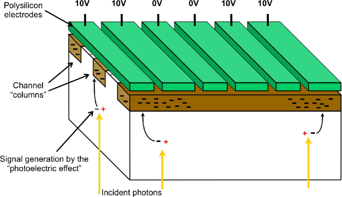
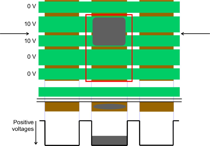
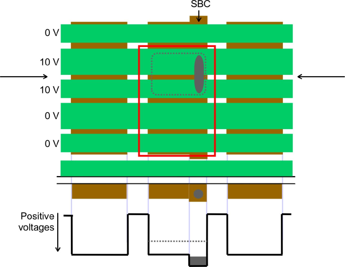
Fig. 3 illustrates the general principles of the Gaia CCD. Buried Channels (BCs) and SBCs are introduced in Figs. 3 and 3 respectively. Once the SBC FWC is reached, any further charge spreads out to cover the whole BC volume, as shown by the dotted lines in Fig. 3.
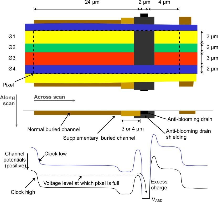
The CCD91-72 was designed and manufactured by e2v especially for Gaia. Gaia has one of most complex pixel architectures built for astronomy (see Fig. 4). It includes the standard BC, the relatively rare SBC and, unusually, an Anti-Blooming Drain (ABD). Gaia is the only astronomical detector with an ABD. It prevents charge bleeding down columns from bright observations, allowing simultaneous faint observations. The ABD also removes excess charge from just upstream of TDI gates. These gates, located at different positions within each CCD, block charge packets of very bright observations that would otherwise saturate the pixels. This allows their integration to begin just downstream of the TDI gate at shorter distances from the readout register.
The doping that defines each pixel feature is implanted into the CCD silicon using a photo-lithographic mask. Each feature (e.g. BC or SBC) has its own mask. Due to practical manufacturing constraints, the masks are smaller than the image area of large format devices like the Gaia CCD (4.5 cm 5.9 cm). The mask area dictates the area of the CCD over which the photoresist layer can be patterned at any one time. This smaller sub-array is called a stitch block (de Bruijne 2008, see Fig. 5). Large format devices like the Gaia CCD are fabricated using a photo-lithographic ‘step and repeat’ process that patterns the photoresist for a particular pixel feature simultaneously everywhere in a stitch block, one stitch block at a time. After the entire wafer has been patterned a single ion implantation process is performed.
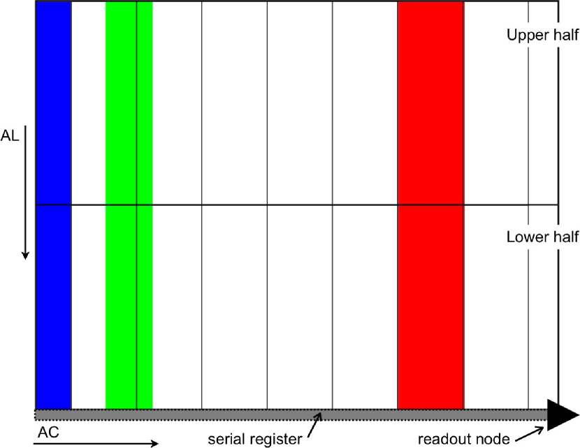
Both Gaia CCD’s upper and lower halves are photo-lithographically stitched from 7 repeated stitch blocks and 2 end-termination stitch blocks. A Gaia CCD is thus composed of 18 different stitch blocks. Each termination stitch block contains 108 columns while each repeated stitch block section contains 250 columns: columns in the ACross scan (AC) direction and 4500 TDI lines in the ALong scan (AL) direction. The AL direction refers to the scan direction of stars along Gaia CCD columns that is induced by the continuous spinning of the spacecraft around its own axis.
In the CCD upper half (cf. Fig. 5) the nominal SBC doping width is 3 m, whereas in the CCD lower half the nominal SBC doping width is 4 m (Burt 2003). This is because every CCD column and so every SBC crosses the horizontal stitch boundary. The SBC doping width is increased immediately after the stitch boundary to minimise the possibility of the SBC narrowing at the boundary as it is known that boundaries can cause the formation of potential pockets, which act like radiation traps, capturing and then releasing electrons and thus increasing CTI. This difference between the nominal SBC doping widths in the upper and lower halves of each Gaia CCD translates to different SBC FWCs in either half.
3 First Pixel Response measurements
3.1 Technique
The FPR measurement consists of the analysis of the charge loss (induced by trapping) that occurs in the first pixels of a well-characterized signal after its transfer across the full CCD image area. By well-characterized signal, we mean a signal for which the shape and the number of charges can be inferred independently from the CTI effects such as for a CI.
In the first pixel row only, the Gaia CCD pixels comprise a diode to generate artificial charges and a gate to control the number of artificial charges injected i.e. effectively transferred across the CCD (cf. appendix for more details about charge injection techniques). During the Gaia mission, CIs will be performed periodically (every 1 s) by blocks of 4 to 20 lines to fill a large fraction of the traps prior to the stellar transits and thus mitigate the CTI effects.
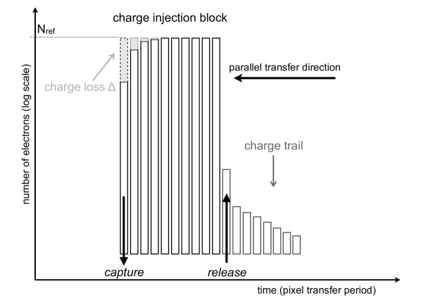
As depicted in Fig. 6, in a CI block of several tens of lines, the first line undergoes the most damage by encountering a certain fraction of the total amount of active traps (i.e. the empty traps) present in the signal confinement volume. As we shall see this fraction depends on the CI level (the number of electrons per pixel in the CI block) and the electron density distribution within a pixel. Depending on the capture cross-section of the trap species present and the clocking rate, the first CI line may not fill all the encountered traps. This is also because the first CI line is losing signal along each CCD column as charge is captured. In this case the second CI line will also experience charge loss and subsequently for the other lines of the CI block. After a certain number of lines, no significant trapping can be measured. Using the last lines of a CI block one can measure a reference CI level, , and thus compute the charge loss (i.e. the total number of trapped charges), and the fractional charge loss :
| (1) | |||
| (2) |
where is the number of pixel-1 in the line of the CI block. The traps filled by the CI with a release time constant shorter than the CI block duration will release electrons within the CI block and can thus bias the measurement of the CI reference level. To minimize this source of uncertainty only the first line(s) of the CI block should be considered in the charge loss measurement. The charge loss measured in the first lines of a CI block depends on the state of the traps at the time they are encountered by the CI signal. The trap state is set by the CCD illumination history. During a FPR experiment, it is thus important to have a good control (or at least a good knowledge) of the CCD illumination history. In the FPR experiments carried out by Hopkinson et al. (2005) to characterize the effect of the SBC, two CI blocks were performed with 100 lines of delay between them. The first CI block was performed to reset the illumination history, and only the second block was used to measure the charge loss. The level of the first block was fixed to , while the level of the second block was varied. In this way, one can study the charge loss variation as a function of signal level which enables the characterization of the SBC within a CCD pixel column. Only the first pixel was taken into account in the fractional charge loss measurement.
3.2 Selection of the data
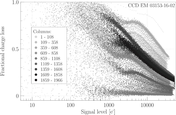
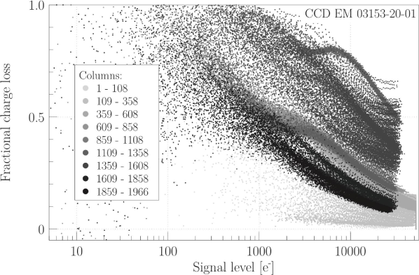
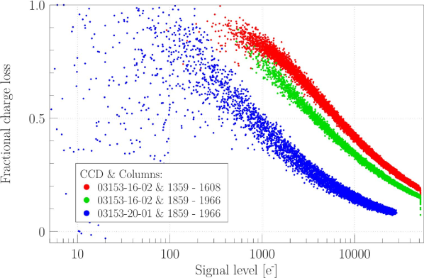
The first set of CCD radiation test data obtained by an industrial partner in the Gaia project was by Sira. These electro-optics tests were carried out on seven Gaia Astrometric Field (AF) DM and EM CCDs (see Table 1) and are described in Hopkinson et al. (2005) and Hopkinson (2006). Hopkinson (2006) figs. 8-2-2 and 8-2-3 show FPR data from different columns from different AL stitch block couples. The top two plots in Fig. 7 group these data into AL stitch block couples for two of these CCDs. The majority of the AL stitch block couples exhibit a characteristic bump in their fractional charge loss curves. This bump is due to SBCs.
At the leftmost (smaller signal level) inflexion point in these fractional charge loss curves, the number of electrons in the SBC start to collapse the SBC potential so some of these electrons spill out of the SBC potential into the BC potential. No longer protected in the smaller volume of the SBC, these few electrons in the BC meet more traps, causing the fractional charge loss increase. At the rightmost (larger signal level) inflexion point, the signal level has completely collapsed the SBC potential into the BC potential so here the SBC potential well no longer exists and all the electrons sit in the BC potential. The presence of SBCs causes the fractional charge loss curve to shift left to smaller signal levels so that at a given signal level the fractional charge loss in the SBCs is less than it would be in the BCs.
We visually examined the fractional charge loss curve of every AL stitch block couple in each of the seven CCDs and found three examples from two CCDs that do not exhibit the characteristic SBC bump (see bottom plot of Fig. 7). It was decided to model the AL stitch block couple that had FPR data extending to the smallest signal levels (EM 03153-20-01 columns 1859–1966, see Fig. 5 blue area) to provide more modelling constraints. The other two examples show hints of turning over into the characteristic SBC bump where their data stops. In the next section, we model this data to test our hypothesis that a fractional charge loss curve without a bump indicates a reduced SBC FWC.
| Serial Number | Model (Extra information) |
|---|---|
| 03153-05-02 | DM (front illuminated) |
| 03153-07-01 | DM (front illuminated) |
| 03153-16-02 | DM |
| 03153-20-01 | DM |
| 03442-11-01 | EM |
| 03483-05-02 | EM |
| 03483-06-02 | EM |
3.3 Generation of the synthetic data
3.3.1 Simulation setup
In order to reproduce the FPR measurements, we simulate the transfer of a CI block over the image area of a virtual irradiated CCD using the detailed Monte-Carlo model of charge transfer presented by Prod’homme et al. (2011)333This model can be used as part of the Java package CEMGA available online: http://gaia.strw.leidenuniv.nl/cemga. This model was verified against experimental data acquired with Gaia irradiated CCDs. In particular, by using a flexible and analytical representation of the electron density distribution, Prod’homme et al. (2011) were able to accurately reproduce the measurement of fractional charge loss as a function of signal level in the presence of SBCs (in both CCD halves).
As already mentioned the SBC confines the electron packet in depth () and in the AC direction (), but the packet remains spread under two electrodes in the parallel transfer direction () independently of the signal regime. Thus, in the model, the SBC and BC signal confinement volumes have different dimensions along and (, , , and ), but the same size along (). Accordingly the centre and the standard widths of the density distribution along and are different for the BC and SBC regimes. For each regime, the distribution standard width in one direction is set to a fraction of the signal confinement volume dimension in that direction, e.g.: . In this way the ratio between the dimensions of the signal confinement box is preserved in the electron density distribution. A larger means a larger spread in electron distribution. is thus later referred to as the electron density distribution spread factor.
Like in Prod’homme et al. (2011), the BC signal confinement volume and the standard widths of the electron density distribution remain the same for the two CCD halves. Prod’homme et al. (2011) modelled a single set of SBC parameters in both CCD halves. However, as explained in Section 2, the SBCs have different doping widths in each CCD half and so should have different values of and FWCs () in each CCD half. This more realistic modelling is the main difference between the simulation in Prod’homme et al. (2011) and the one in this paper. Therefore, in this paper , and are free parameters in the model, where 1 is the CCD upper half (furthest from the readout register) and 2 is the lower half.
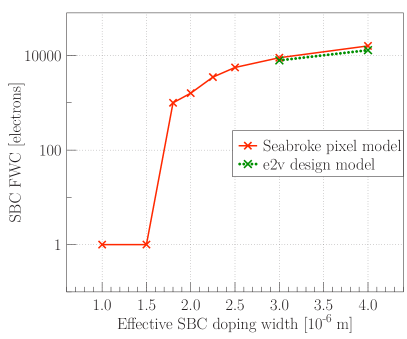
The nominal SBC doping width is 3 m in the upper half and 4 m in the lower half. If the SBCs are undisturbed in the pixel, one would expect to be similar widths. However, as shown in Section 2, the SBCs are not undisturbed: they are adjacent to ABDs. A 3D semi-conductor physics model of the Gaia pixel (Seabroke et al. 2010) finds that ABDs reduce the nominal SBC doping widths to effective SBC doping widths () and thus also reduce . Fig. 8 shows that m yield simulated SBC FWCs of 10 000 electrons. The bottom plot of Fig. 7 shows that our candidate reduced SBC FWC AL stitch block couple does not exhibit a SBC bump near 10 000 electrons. Therefore, a more realistic constraint on for this particular simulation is 2 m. This corresponds to a maximum SBC FWC of several 1000 electrons.
The transition between the two signal regimes occurs at . It is important to note that although in reality the model parameter would be equated to the real SBC FWC, in the model used, due to the arbitrary nature of the chosen description for the transition between the BC and SBC regimes, gives only an indication about the real value of the SBC FWC (see Prod’homme et al. (2011) for more details).
During the experiments carried out by Hopkinson, two CI blocks were transferred. The first CI block was used to reset the illumination history by filling a large fraction of the empty traps. The second block was used to perform the FPR measurement and its level varied. For most of the tested levels, the level of the first block (30 000 pixel-1) was higher than the level of the second. As a consequence the population of traps probed by the second CI block was the same as for the first. However from this population the only traps capable of capturing electrons from the second block, are by definition the empty traps: the ones that were able to release their electron before the crossing of the second block. In our simulated experiment we can thus simulate the transfer of a single CI block (of 20 lines) crossing the image area of a CCD containing only empty traps and perform the FPR measurement on this very same CI block. As for this particular experiment we are interested in the electron capture only, we used a unique trap species with a common capture cross section ( = 510-16 cm2) and a long release time constant compared to the duration of the CI (20 0.9892 ms) such that the charge loss and the reference level measurements are not biased by a significant release of electrons.
The simulated CCD image area consists in a single column of 4500 pixels. We did not simulate the transfer across the serial register, as one can to first order ignore the effects of the serial CTI. Once the CI block is transferred through the two CCD halves, the FPR measurement is performed in the same way as for the experimental test (Section 3.1). For each set of simulation parameters, the CI level is varied from 50 to (with , , , , , , , as intermediate values).
3.3.2 Model to data comparison
In our simulations, there are six free parameters:
-
1.
, and the electron density distribution spread factors, that set the standard widths of the electron distribution for each signal regime and CCD half according to the signal confinement volume dimensions,
-
2.
and the signal level at which the transitions between the SBC and BC regimes is performed,
-
3.
the number of traps per pixel.
Table 2 details all the simulation parameters and indicates the values we used for the fixed parameters as well as the allowed intervals for the free parameters.
We are not interested in the exact reproduction of the data but rather in the study of the parameters of the electron density distribution model that lead to a reasonable agreement between the simulated and the experimental fractional charge loss measurements over the studied range of CI signal levels. We thus generate random sets of parameters in order to probe homogeneously the entire parameter space. Each parameter set results in a set of data points that sample the simulated fractional charge loss curve. These data points are then compared to the experimental measurements. To proceed to this comparison, we have first generated an analytical representation of the experimental data by the mean of a fit using spline functions. We use the analytical fit values and the simulation results at each particular signal level to compute the , that constitutes our comparison criterion:
| (3) |
where is the total number of simulated CI levels and the noise. We use the formal errors associated to the analytical fit to the experimental data as values and thus assume that the formal errors encompass the experimental noise and the readout noise.
| Parameter | Description | Fixed value or interval |
|---|---|---|
| T | temperature | 163 K |
| PTDI | TDI period | 0.9828 ms |
| number of traps per pixel | – | |
| capture cross section | 5 m2 | |
| release time constant | 9 s | |
| BC regime | ||
| distribution spread factor | – | |
| BC FWC | ||
| BC signal confinement volume size: | ||
| in the AL direction | 11 m | |
| in the AC direction | 24 m | |
| in depth | m | |
| SBC regime | ||
| distribution spread factor: | ||
| in the CCD upper half | – | |
| in the CCD lower half | – | |
| SBC to BC regime transition signal: | ||
| SBC FWC in the CCD upper half | – | |
| SBC FWC in the CCD lower half | – | |
| SBC signal confinement volume size: | ||
| in the AC direction | 2 m | |
| in depth | m | |
3.4 Comparison results
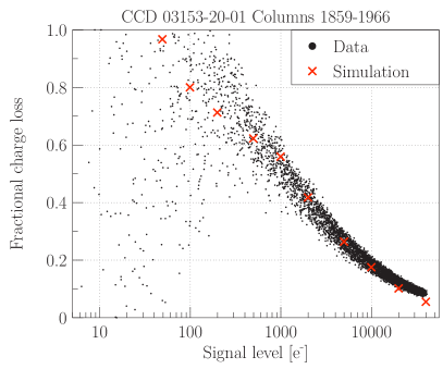
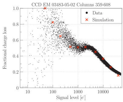
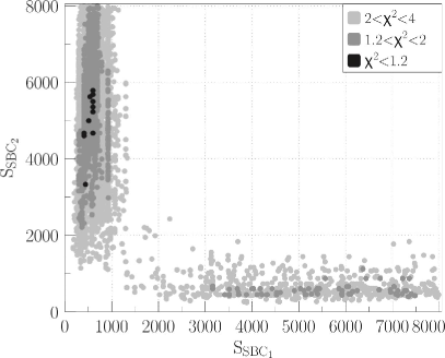
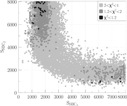
Fig. 9 shows the fractional charge loss measurement (first line of the CI considered only) carried out by
Hopkinson (black dots) on the Gaia AF CCD EM 03153-20-01 for the columns 1859 to 1966 (left panel) and on the Gaia AF CCD EM 03153-16-02 for the columns 609 to 858 (right panel) along with the result of the
presented simulation setup that aimed to reproduce these measurements (red crosses). The simulations shown
are representative of the best fit to the data that can be obtained following a semi-random search444A genetic algorithm was used as an optimization procedure - see
http://watchmaker.uncommons.org/ in the
parameter space for both investigated cases: suspected reduced SBC FWCs (left) and a typical SBC FWC case (right).
Fig. 10 shows that the fit for the two cases occupies different regions of parameter space, as expected given the differences in Fig. 9. The most likely solutions are where e- or e- for the typical SBC FWC case but where e- or e- for the reduced SBC FWC case. From the figures it also appears that there are more solutions with low for . In principle the two cases should be distinguishable because it matters which SBC FWC comes first. Of course with the data available the distinction is not so easy to make. However, as should always be smaller than , we consider the e- solutions in both cases to be unphysical.
The first verification that SBCs are present in Gaia CCDs by finding the characteristic bump in the FPR curve was also the first published estimate of Gaia’s SBC FWC (Hopkinson et al. 2005). Fig. 9 (right) plots includes the same data as their fig. 11. They estimated the SBC FWC to be 1400 . However, this is a typographical error in their paper. The arrow defining their SBC FWC in their fig. 11 is pointing to 1400 ADU, which corresponds to 1100 . Fig. 9 (right) shows that this signal level corresponds to the first inflexion point. This paper is the first time a FPR curve has been modelled taking into account the different SBC FWCs in a Gaia CCD. e- in Fig. 10 (right) corresponds to a point in between the inflexion points in Fig. 9 (right), whereas e- does not correspond to any part of the inflexion. Therefore, the characteristic bump is at signal levels that correspond to the smaller upper half SBC FWC and not the larger lower half SBC FWC.
Because of the way e2v manufacture the CCDs (all the SBC doping implanted simultaneously), intra-stitch block SBC FWCs in a particular half should be the same. However, in the Gaia case, there is no guarantee that inter-stitch block SBC FWCs will be the same. This is due to the SBC doping abutting the ABD doping (see Fig. 4 top schematic) and overlapping the ABD shielding doping (see Fig. 4 middle schematic). The ABD doping is the first pixel feature to be implanted into each pixel within a stitch block area of CCD silicon using its own photo-lithographic mask (the size of a stitch block). The ABD mask is aligned to the ‘zero grid’. All the SBCs in all stitch blocks have their doping implanted subsequently using a SBC photo-lithographic mask aligned to the same zero grid. Each mask alignment to the zero grid is subject to random alignment (stitch) errors of 0.25 m (Burt 2005a). Because the ABD shielding doping cancels out the SBC doping, the effective SBC doping width, consequent potential depth and resulting FWC is sensitive to the stitch error. Therefore, scatter in inter-stitch block SBC FWC (both intra-CCD and inter-CCD) is expected from the nominal e2v design of the Gaia CCDs, as seen in Fig. 7.
The SBC FWCs of the typical case are much smaller than e2v’s analytical Gaia CCD design predictions (published for the first time in Seabroke et al. 2010): 7900 in the upper half and in the lower half, which correspond to m. Inputting m to the Seabroke et al. (2010) pixel model successfully reproduces e2v’s analytical predictions (see Fig. 8). This figure suggests this is not due to random stitch errors (worst-case random alignment stitch error = 0.5 m) as these would result in m, which does not reduce the SBC FWCs to the model fit of . To do this requires a systematic shift to m555 m is larger than m. Nevertheless, Fig. 9 (left) shows that the simulation is able to reproduce the FPR data very well.. This m from the design appears to be uncalibrated systematic offsets in e2v photo-lithography, which could either be due to systematic stitch offsets or ABD shield doping diffusion in the AC direction. The Seabroke et al. (2010) pixel model does not specifically simulate either of these scenarios, rather it simulates a that could be produced by both or either of these scenarios.
The best fit in Fig. 10 (left) is , which are indeed reduced SBC FWCs compared to the typical case by a factor of 3 in the upper half and a factor of 2 in the lower half. This corresponds to m. The difference with the typical case is m. Because this AL stitch block couple consists of termination stitch blocks, it is possible that this is a rare example of compounding stitch errors starting from the typical SBC FWC case.
4 Pocket pumping measurements
4.1 Technique
The determination of SBC FWCs in both halves of Gaia CCDs in the previous section required simulations to interpret measurements of charge packets that had traversed both halves of the CCD (FPR) in terms of SBC FWC in each half. Pocket pumping can provide a direct measurement of the SBC FWC in each half. Charges from a flat field illumination are moved back and forth in the image area over a one pixel length. In pixels with traps, single electrons can be statistically trapped during one half-cycle and then released during the next half-cycle into the adjacent pixel. This produces bright-dark pairs around the mean flat field level at the trap position. Repeating the technique with increasing mean flat field signal levels identifies the number of traps per pixel as a function of signal size.
4.2 Devices tested
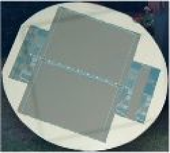
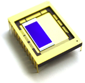
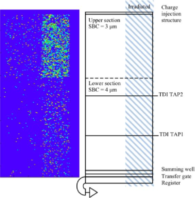
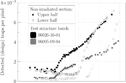
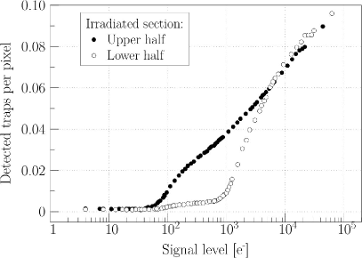
Fig. 13 shows that each e2v Gaia silicon wafer can only include two Gaia CCDs (CCD91-72). The room left on each wafer was used for test structures that were included to assess the radiation hardness of Gaia CCDs. In order for these test structures to be irradiated and tested, they have to be packaged. e2v packaged up two CCD221 test structures for the e2v centre for electronic imaging at The Open University to test (see Fig. 13). Because they have the same pixel architecture (and thus manufacturing processes) as Gaia CCDs, we have repeated the pocket pumping measurements conducted by Kohley et al. (2009) (hereafter K09) to test whether these test structures also have reduced SBC FWCs. K09 tested an AF FM CCD with serial number 05486-11-02. The test structures are also post-2004 but from two different batches: 06026-16-04 and 06095-09-04. The last two digits are the position of the device on the wafer: 03 and 04 are the two right side positions for the CCD221 test structures (see Fig. 13). 06026-16-04 was irradiated (see Fig. 13). 06095-09-04 was not irradiated.
All CCD221 test structures have 1440 TDI lines and 224 columns, which is smaller than one Gaia stitch block (2160 or 2340 TDI lines and 250 or 108 columns). The CCD221 is not stitched during manufacture i.e. its image area consists of only one stitch block but the SBC doping has a width change (at the dotted line in Fig. 13) to replicate the width transition at the AC stitch boundaries in CCD91-72’s. This means the CCD221 test structures cannot be used to compare stitch blocks in different AC positions as was done in K09.
4.3 Results
The top of Fig. 15 shows that the number of identified fabrication traps per pixel in both test structures is the same order of magnitude as seen in by K09 (see their fig. 9). It also shows that there are an order of magnitude more radiation traps per pixel as there are fabrication traps per pixel. Nevertheless, the same trends as a function of CCD half are seen in both the non-irradiated and irradiated parts of 06026-16-04. The lower half trend as a function of signal size in this device is that signals have a very different gradient to signals . The lower half trend as a function of signal size in the other device (06095-09-04) is similar: signals have a very different gradient to signals . We interpret the change in gradient as due to electrons spilling out of SBCs in the lower halves of these devices with FWCs of 1000 and 3000 respectively. K09 found exactly the same spread of SBC FWCs between the AL stitch block couples in their CCD. It suggests that both test devices and the K09 CCD all have between 1.75 and 2.25 m (see Fig. 8).
Like K09’s fig. 9, the upper halves of our test structures do not exhibit a change in gradient at . Instead the upper half trend as a function of signal size in both devices is that signals have a very different gradient to signals . We interpret the change in gradient as due to electrons spilling out of SBCs in the upper halves of these devices with FWCs of 50 . K09’s smallest signal level of did not find the change in gradient, suggesting the upper half SBC FWC of this CCD is 40 . This is consistent with our findings because even a sample random stitch error can result in a large change in SBC FWC because the SBC FWC- relation is steep at this signal level. Such small SBC FWCs may not be physical because the SBC potentials would be very shallow, allowing electrons to thermally diffuse out. Whether the upper half SBC FWCs in these devices is zero or tens of electrons, these SBC FWCs are very much reduced compared to their lower halves and compared to pre-2004 CCDs.
The post-2004 devices have m, which is different to the typical pre-2004 devices with m ( m) and very different to the design with m ( m, see Fig. 8). Again, this appears to be uncalibrated systematic offsets in e2v photo-lithography but larger in magnitude than the pre-2004 offsets.
5 Comparison of EADS-Astrium Radiation Campaigns 3 and 4 test data from the same CCDs
EADS-Astrium have carried out a series of five test campaigns on a small number of irradiated CCDs in order to evaluate the impact of radiation damage on the image parameter estimation and ultimately on the Gaia astrometric performances. Table 3 provides a summary of the CCDs tested during these campaigns. The tests were carried out using a number of runs of an illuminated mask along the CCD which is operated in TDI mode. A number of different masks were used throughout the testing campaigns, each with a different pattern of pin-holes (of sometimes differing diameters). The location and flux biases are generally calculated through a comparison of data acquired from an irradiated portion of the CCD with an non-irradiated portion of the same device.
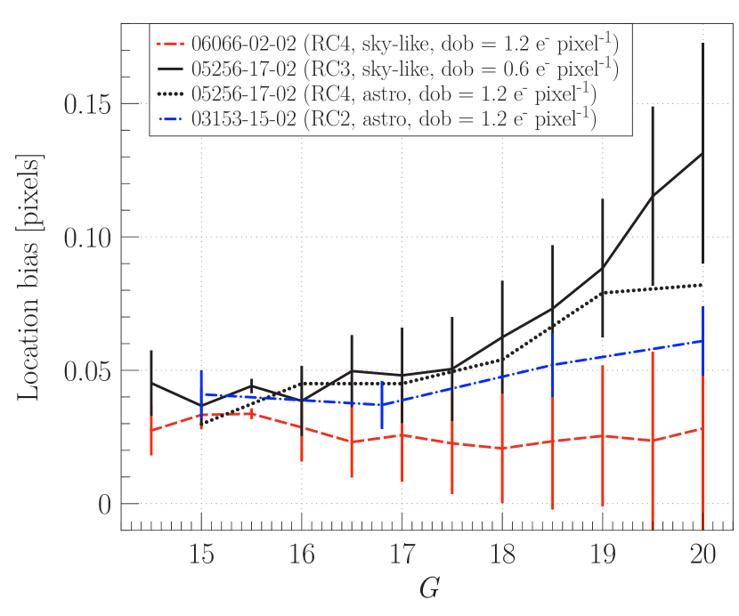
The resulting bias measurements shown in Fig. 15 differ between RC2, RC3 and RC4 at faint magnitudes: the RC3 data does not plateau to an approximately constant bias at faint magnitudes. This is in contrast to the data from the other campaigns. One possible reason for the RC3 bias values not plateauing is due to the presence of the constant Diffuse Optical Background (DOB) being better controlled in the experimental setup of RC3 compared to RC2 and RC4. When the DOB is very close to zero, then just a small amount of background light can drastically reduce the image location bias due the resulting photo-electrons keeping many of the traps with long time constants (or ‘slow’ traps) filled. Indeed, the measured DOB levels are 0.6 pixel-1 lower in the RC3 data than in RC4. However, RC4 data taken with the same CCD as was used in RC3 shows a similar bias function to RC3 (i.e., no plateau at faint magnitudes) and in this case the DOB level is comparable to both the RC2 and RC4 data set with another CCD. It thus appears that the DOB level is not the primary cause of the discrepancies between the location bias functions across the different test campaigns. This hypothesis is further strengthened when one considers that these data were obtained with a CI implemented every second, which also has the effect of keeping the ‘slow’ traps filled, and making the effect of small levels of DOB much less significant.
The most likely conclusion is that the measured differences are intrinsic to the CCDs. Fig. 15 shows that 03153-15-02’s location bias as a function of brightness is in between the plateau of 06066-02-02 and 05256-17-02. Prod’homme et al. (2011) modelled the FPR curve in different AL stitch block couples in 03153-15-02 from a single non-uniform CI using a single SBC FWC for both halves of the CCD. They found the SBC FWC to be 2825 electrons. Given that Section 3.4 suggests that the shape of the FPR curve is dominated by the upper half SBC FWC, we can assume the SBC FWC in the upper half of 03153-15-02 is approximately 2825 electrons. The typical pre-2004 case in Section 3.4 has SBC FWCs of 1509 electrons. Both this value and 2825 electrons are consistent with m, which corresponds to (see Fig. 8). Therefore, we also consider 03153-15-02 to be a typical pre-2004 case and so not have reduced SBC FWCs.
The SBC FWCs of 06066-02-02 and 05256-17-02 have not been measured. Nevertheless, the fact that Fig. 15 shows that the location bias of 06066-02-02 is smaller than 03153-15-02 suggests that the 06066-02-02 SBC FWCs are larger than 03153-15-02’s because they are protecting small charge packets from CTI more than 03153-15-02. This is the first evidence that not all post-2004 CCDs have reduced SBC FWCs compared to the typical pre-2004 CCD. Following the same argument, the fact that Fig. 15 shows that the location bias of 05256-17-02 is larger than 03153-15-02 suggests that the 05256-17-02 SBC FWCs are smaller than 03153-15-02’s because they are protecting small charge packets from CTI less than 03153-15-02. However, whether 05256-17-02 SBC FWCs are the same as all the other post-2004 SBC FWCs measured in Section 4 is an open question.
| Serial Number | Variant | Reduced SBC FWCs |
|---|---|---|
| 03153-15-02 | AF DM | No |
| 05256-17-02 | AF EM | Yes? |
| 06066-02-02 | AF EM | No? |
| 06244-03-01 | RP DM | ? |
| 06273-08-01 | RP EM | ? |
6 Discussion
6.1 Comparison of pre- and post-2004 CCD samples
We consider evidence from the pre-2004 and post-2004 CCDs separately because FM CCDs only will be flown on Gaia and all FM CCDs were built post-2004. Because of the low number of CCDs that have been tested, we augment our evidence found in this paper with evidence from the literature.
6.1.1 Pre-2004 CCDs
From the Sira test sample, out of the seven 2003 AF CCDs searched for evidence of reduced SBC FWCs in Section 3, we only find one CCD with one stitch block AL couple (termination stitch block with 108 columns) strongly suspected of not having reduced SBC FWCs compared to the typical case (by one order of magnitude in the upper stitch block). We augment this pre-2004 CCD sample with the first device tested by EADS-Astrium, an AF DM (03153-15-02) that exhibits typical SBC FWCs in upper half stitch block couples. Thus, a reduction in upper half SBC FWCs by one order of magnitude affects the pre-2004 CCD sample as follows:
-
•
1 out 8 CCDs % of CCDs;
-
•
1 out of () 72 stitch block AL couples in 8 CCDs 1.4% of stitch block AL couples;
-
•
108 out of [8 ] columns in 8 CCDs 0.7% of columns.
This small number of columns with reduced SBC FWCs in their upper halves is consistent with accumulating stitch errors at each of the eight inter-stitch block AC alignments being a rare event, mainly in the termination stitch blocks furthest from the readout node.
6.1.2 Post-2004 CCDs
In Section 4, we found two CCD221 test structures (224 columns in each device) with reduced SBC FWCs in their upper stitch blocks compared to the typical pre-2004 case (by two orders of magnitude). To these we add the device tested by Kohley et al. (2009) (where all 9 stitch block AL couples were tested). Thus, a reduction in upper half SBC FWCs by two orders of magnitude affects the post-2004 CCD sample (that have had their SBC FWCs measured) as follows:
-
•
3 out 3 CCDs % of CCDs;
-
•
() 11 out of () 11 stitch block AL couples tested in 3 CCDs 100% of stitch block AL couples;
-
•
() 2454 out of () 2454 columns tested in 3 CCDs 100% of columns.
This suggests that a rare compounding of stitch errors is not responsible for the reduction of SBC FWCs in the post-2004 sample but a systematic effect in e2v photo-lithography. Posing the more general question of how many post-2004 devices show any direct or indirect evidence for a reduction in SBC FWCs compared to the typical pre-2004 SBC FWCs allows us to include the two post-2004 devices have been tested by EADS-Astrium in their RCs:
-
•
4 out 5 CCDs % of CCDs;
-
•
() 13 out of () 18 stitch block AL couples tested in 5 CCDs 72% of stitch block AL couples;
-
•
() 2914 out of () 4164 columns tested in 5 CCDs 70% of columns.
6.1.3 Comparison conclusion
It is clear that the pre- and post-2004 CCD samples are systematically different, despite the small sample sizes. The systematic difference is in the typical SBC FWCs for each sample. The pre-2004 sample typically has upper half SBC FWCs of thousands of electrons, with only one exception of 400 electrons. The post-2004 sample typically has upper half SBC FWCs of tens of electrons (or zero), with only one exception of indirect evidence of thousands of electrons. This points to a change in e2v manufacturing of Gaia CCDs between 2003 and 2005. A different mask set is the only known change in e2v manufacturing of Gaia CCDs between 2003 and 2005. However, this can only be considered as circumstantial evidence to explain any systematic changes between pre- and post-2004 CCDs because it would be very difficult to definitively prove the mask set was responsible due to a plethora of other factors that go into manufacturing CCDs with complex pixel architectures.
In the introduction we asked the question: are the SBC FWCs in Gaia CCDs used to predict the faint star ( mag) astrometric performances and against which mitigation models are being developed and tested representative of the CCDs that will fly on Gaia? 03153-15-02 was used for these activities. However, this paper has shown its upper half SBC FWC to be typical of the pre-2004 sample. The pre-2004 sample does not appear to be representative of the CCDs that will fly on Gaia (the post-2004 sample). This means the SBC FWCs of 03153-15-02 also may not be representative of the actual SBC FWCs on Gaia. The 03153-15-02 SBC FWCs were used in the image location estimation in the presence of radiation damage in Prod’homme et al. (2012), which were used in Holl et al. (2012) to investigate the effect of image location errors on the astrometric solution. Hence, it is not known how representative of the whole focal plane these predictions are.
6.1.4 Predicting the SBC FWCs of Gaia’s onboard CCDs
SBC fabrication occurs during front-face processing, which is when the electrodes are made and all doping implanted and is batch based. Because all the Gaia CCDs have the same pixel architecture, front-face processing is the same for all Gaia CCDs: AF, Blue Photometer (BP), Red Photometer (RP). e2v and EADS-Astrium refer only to these CCD variants as the Radial Velocity Spectrometer (RVS) CCDs are identical to RP CCDs. Each CCD serial number encodes when the front-face processing occurred. The fact that all wafers in a batch have the same nominal front-face processing means that if a CCD of any type is found to be affected by reduced SBC FWCs, then it is possible that all the CCD variants (AF, BP and RP) from that batch may also be have reduced SBC FWCs. Table 4 summarizes all the post-2004 CCDs from which SBC FWCs have been derived and their batch numbers. It shows they are all from different batches so whether other CCDs from the same batch are also affected remains unproven (none of the other CCDs that could be tested are from these four batches either). In the absence of evidence demonstrating that all CCDs from the same batch have the same SBC properties, we cannot attempt to predict the SBC FWCs of CCDs onboard the Gaia satellite (post-2004 FMs).
| Method | Variant | Serial Number | Batch Number | ||
|---|---|---|---|---|---|
| RC3&4 (this paper: re-analysis) | AF EM CCD | 05256-17-02 | 05256 | ? | ? |
| PP (K09: 1st measurement & analysis) | AF FM CCD | 05486-11-02 | 05486 | 1000-3000 | |
| PP (this paper: 1st measurement & analysis) | AF FM test structure | 06026-16-04 | 06026 | 50 | 1000 |
| RC4 (this paper: re-analysis) | AF EM CCD | 06066-02-02 | 06066 | ? | ? |
| PP (this paper: 1st measurement & analysis) | AF FM test structure | 06095-09-04 | 06095 | 50 | 3000 |
6.2 Impact on the Gaia image location accuracy
Given that we cannot predict the SBC FWCs of CCDs onboard the Gaia satellite (post-2004 FMs), we simulate all the possible different SBC FWC scenarios to compare their potential impact on the Gaia image location accuracy. Prod’homme et al. (2012) fig. 23 shows that they have already simulated the no SBC scenario, (, and the “Functional SBC” scenario. The latter uses a single SBC FWC derived from 03153-15-02: electrons. In this paper we have found two other scenarios:
-
1.
The apparently rare pre-2004 scenario of one order of magnitude reduction of SBC FWCs compared to the typical pre-2004 case: electrons,
-
2.
The apparently common post-2004 scenario of two orders of magnitude reduction of the upper half SBC FWCs compared to the typical pre-2004 case: electrons,
The simulations of image location accuracy use the same model (Prod’homme et al. 2011) as the simulations of the FPR curve in Section 3, which includes the same parameterisation of the electron density distribution. For scenario (i), the SBC FWC and electron density distribution spread factor () of both halves of the CCD are derived directly from the simulation of the FPR curve and and so form the input to simulate the image location accuracy. In contrast, for scenario (ii) the SBC FWCs are not derived using the model so only the SBC FWCs are available as input to the model but not . Because the in (i) is the closest in value to in (ii), the in (i) is our best estimate for (ii) and so we use this. We use the SBC FWC and values from Prod’homme et al. (2011) as and in scenario (ii) because they are similar to the lower half SBC FWCs found in Section 4.
Gaia has been designed to perform absolute astrometric measurements at very high accuracy. As the estimated image location for all CCD observations are ultimately used to derive the stellar astrometric parameters, the requirements on the image quality are very stringent. Radiation damage distorts the image and decreases the signal-to-noise ratio. While the image distortion, if not properly taken into account, introduces a significant bias (e.g. Fig. 15) in the image location estimation, the decrease in signal-to-noise ratio implies an irreversible loss of accuracy independent of any estimator.
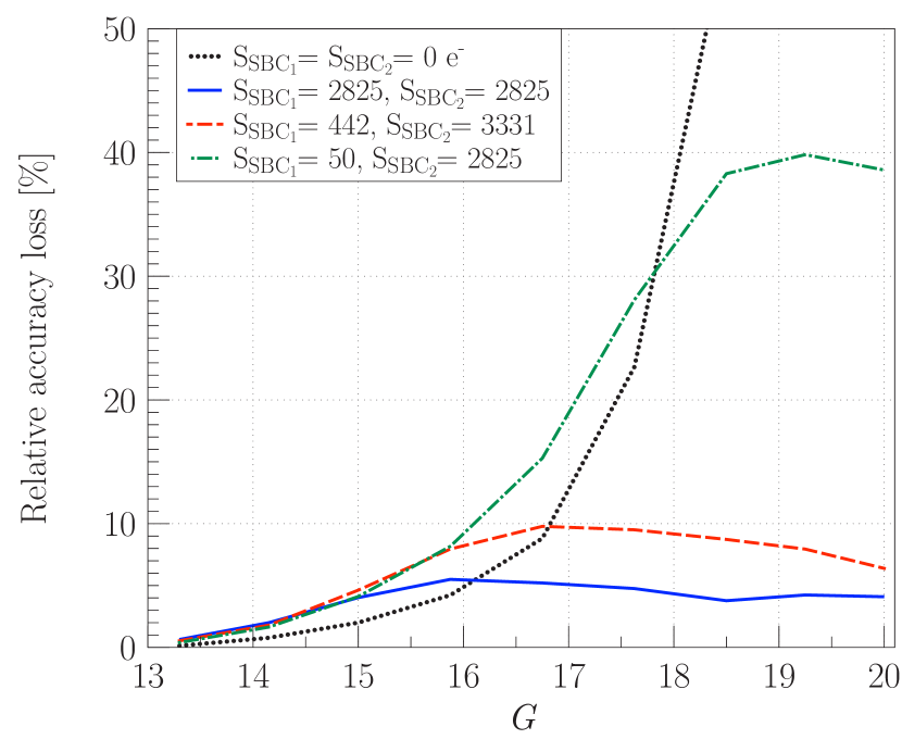
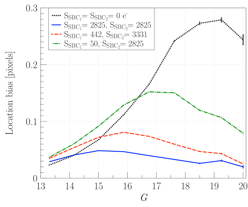
Fig. 17 shows the relative loss of accuracy in image location as a function of stellar magnitude. This is computed by comparing the theoretical limits (the Cramér-Rao bounds) to the image location accuracy for a damaged and a CTI-free Gaia-like image. Zero loss of accuracy corresponds to the CTI-free case (for more details see Prod’homme et al. 2012). Fig. 17 shows the image location bias as a function of stellar magnitude. It is obtained by applying the Gaia image location procedure to several hundreds of profiles without applying any CTI mitigation procedures, the bias itself is computed by subtracting the true from the estimated location. Figs. 17 and 17 provide a comparison for the five different scenarios described above. For the simulation we used a DOB that corresponds to the expected average sky brightness of 2.0 pixel-1 at readout and an active trap density of 1 trap pixel-1. This particular density was shown (Prod’homme et al. 2012) to reproduce the amplitude of location bias measured using experimental test data taken 1 s after a CI and for a Gaia irradiated CCD with a radiation dose of protons cm-2 ( MeV equivalent).
From both figures it is clear that the smaller the SBC FWC, the more the location precision degrades and the greater the bias. Both Prod’homme et al. (2012) and Holl et al. (2012) cite an early draft of this paper, which at that time only included scenario (i) to show that SBC FWCs with hundreds of electrons in their upper half meet Gaia requirements: the CTI-induced loss of accuracy of scenario (i) does not exceed 10 per cent, which is acceptable regarding the Gaia requirements and the CTI mitigation procedure enables a 90 per cent recovery of the bias, bringing back the residual bias of scenario (i) to an acceptable level.
However, with scenario (ii) with SBC FWCs of tens of electrons in their upper half, the bias is a factor of two worse than scenario (i). The bias can in principle be calibrated out by using the same mitigation procedure as foreseen for larger SBC FWCs or the procedure may need to be modified to better model smaller SBC FWCs. The scenario (ii) loss of accuracy is greater than 10 per cent at = 16-17 mag and continues to rise as a function of magnitude to a factor of 4-5 worse than scenario (i) at the faint end. Comparison of Figs. 15 and 17 show that at least one post-2004 CCD (06066-02-02) has a measured bias at the same level as the electrons scenario, which was derived from 03153-15-02 and used by Prod’homme et al. (2012) and Holl et al. (2012) to demonstrate that Gaia meets its astrometric specifications in the presence of radiation damage. Therefore, it is unlikely that all the CCDs onboard the Gaia satellite are like scenario (ii). Even if they are, these simulations are using a radiation dose of protons cm-2 ( MeV equivalent). The latest predicted end-of-life dose is protons cm-2 ( MeV equivalent). Therefore, the bias and loss of accuracy are likely to be overestimated.
The location bias of 05256-17-02 in Fig. 15 is of particular interest because Lindegren & Crowley (2010) carried out a mag astrometric performance analysis of test data acquired using the ‘sky-like’ mask with this particular CCD in which they show that the mission requirements are still met for the faint stars after software radiation damage mitigation has been applied. In Section 4.3, we interpreted its SBC FWCs as being smaller than the typical pre-2004 levels i.e. it is not like scenario (i) but its actual values are currently unavailable. Comparing Figs. 15 and 17 shows that the shape of the location bias of 05256-17-02 as a function of magnitude is different to the simulated scenario (ii), suggesting that 05256-17-02 is not like scenario (ii) either. However, we cannot predict how many CCDs onboard Gaia are like 05256-17-02 so the findings of Lindegren & Crowley (2010) cannot be considered as conclusive proof that Gaia meets its mission requirements.
A more representative faint star astrometric performance prediction depends on knowledge of the SBC FWCs onboard the satellite, which is not known. Therefore, we recommend these should be measured as soon as possible to allow faint star astrometric performance predictions to be updated in case satellite operating conditions or CTI software mitigation can be further optimised to improve the scientific return of Gaia.
7 Conclusions
ESA’s Gaia satellite has 106 CCD image sensors which will suffer from increased charge transfer inefficiency (CTI) as a result of radiation damage. To aid the mitigation at low signal levels, the CCD design includes Supplementary Buried Channels (SBCs, otherwise known as ‘notches’) within each CCD column. We present the largest published sample of Gaia CCD SBC Full Well Capacity (FWC) laboratory measurements and simulations based on 13 devices. We split this sample into pre- and post-2004 because before manufacturing Flight Models (FMs), e2v changed their photo-lithographic mask set in 2004 but the set was meant to be identical to the one used to manufacture the Demonstrator Models (DMs) and Engineering Models (EMs).
The pre-2004 sample consists of eight CCDs: one EM, which had its First Pixel Responses (FPR) analysed by Prod’homme et al. (2011), and seven DMs and EMs, which had their FPRs measured by Hopkinson (2006). We selected a typical and a rare subsample of columns from two of these seven CCDs to model and derive upper and lower half SBC FWCs. The post-2004 sample consists of five devices: one FM, which was pocket pumped by Kohley et al. (2009), two test structures that we pocket pumped and two EMs, the data from which we re-interpreted in terms of SBC FWCs.
We find that Gaia CCDs manufactured post-2004 have SBCs with FWCs in the upper half of each CCD that are systematically smaller by two orders of magnitude (50 electrons) compared to those manufactured pre-2004 (thousands of electrons). Gaia’s faint star ( mag) astrometric performance predictions by Prod’homme et al. (2012) and Holl et al. (2012) use pre-2004 SBC FWCs as inputs to their simulations. However, all the CCDs already integrated onto the satellite for the 2013 launch are post-2004. SBC FWC measurements are not available for one of our five post-2004 CCDs but the fact it meets Gaia’s image location requirements suggests it has SBC FWCs similar to pre-2004. We are now in a position to answer the three questions posed in the introduction:
-
1.
In the absence of testing FM CCD SBC FWCs as a criterion for selecting which CCDs should fly on the Gaia satellite, is it possible to predict how many will have reduced FWCs? All the CCDs from the same manufactured batch should nominally have the same SBC FWCs. However, none of the five post-2004 devices are from the same batch so it is not possible to theoretically predict the SBC FWCs onboard.
-
2.
Are the SBC FWCs in Gaia CCDs used to predict the faint star astrometric performances and against which mitigation models are being developed and tested representative of the CCDs that will fly on Gaia? A pre-2004 CCD with upper half SBC FWCs of 2825 electrons and the post-2004 CCD without knowledge of its upper half SBC FWCs have been used to predict faint star astrometric performances. Given that the onboard SBC FWCs are not known, it is not known whether these CCDs are representative of the CCDs that will fly on Gaia and consequently whether the performance predictions based on these single CCDs are representative of the entire focal plane.
-
3.
What is the impact of reduced SBC FWCs on the Gaia image location accuracy? We quantify the impact of reduced SBC FWCs on the Gaia image location accuracy, which increases the bias and decreases the accuracy. However, these numbers are specific to single CCDs, which may not be representative of the entire focal plane.
It is too late to measure the SBC FWCs onboard the satellite before launch. Gaia’s faint star astrometric performance predictions depend on knowledge of the actual SBC FWCs but as these are currently unavailable, it is not known how realistic these predictions are. Therefore, we suggest Gaia’s initial in-orbit calibrations could include a method, which we present in Section 8, to measure the onboard SBC FWCs. Realistic faint star astrometric performance predictions at the start of the mission would allow satellite operating conditions or CTI software mitigation to be further optimised to improve the scientific return of Gaia.
It should be emphasized that SBC FWCs were never a formally agreed CCD acceptance criterion in the Gaia contract between ESA/EADS-Astrium and e2v, but a design goal. For this reason, it was not systematically tested in the Gaia development phase. Assuming extended testing beyond the agreed CCD acceptance criteria would have found the reduced SBC FWCs in post-2004 CCDs, it certainly remains a challenge for CCD testing in large quantities to detect unexpected design and performance issues. While the discovery came too late for Gaia to implement design changes, it nevertheless provides a very useful feedback for future CCD developments. e2v are also developing the CCDs for ESA’s Euclid satellite (launch 2019), which, despite metrology improvements, will not include SBCs (or anti-blooming drains).
8 Further work
It is too late to measure the Gaia SBC FWCs onboard the satellite before launch. We suggest Gaia’s initial in-orbit calibrations (IIOC) could include a method to measure the onboard SBC FWCs. First Pixel Response (FPR, see Section 3) measurements will be conducted during the IIOC to measure radiation trap properties but with only charge injection (CI) at one level. However, to use FPR to measure SBC FWCs requires many different CI levels (a non-standard procedure), that the CCDs need to have been sufficiently irradiated and that the analysis of the data is model dependent. Pocket pumping (see Section 4) cannot be used now that the FM CCDs have been integrated into the satellite because the clock timing in the FM Proximity Electronics Modules does not allow modification for backwards shifts in the image area. It only works well if the trap density is low, whereas FPR only works well if the trap density is high.
An alternative to measuring SBC FWCs in a more time-efficient and direct method is the minimum charge injection method (MIM). MIM injects charge into the first TDI line only i.e. the first pixel in every column (see Appendix for technical details). Although this single line of charge is transferred through the entire image area of the CCD and read out, it is only designed to be a direct measurement of the SBC FWCs in the first TDI line. Because of the way e2v manufacture the CCDs (all the SBC doping implanted simultaneously), intra-stitch block SBC FWCs should be the same. This paper has shown that the upper half SBC FWCs are more important inputs for simulations than the lower half SBC FWCs.
However, the efficacy of MIM has not been experimentally proven. This could be because MIM works but has only been tested on CCDs with effectively zero SBC FWCs in their upper halves. Alternatively, it could be that the measurement method does not work and so returns a null result regardless of SBC FWC. Therefore we plan to test MIM’s efficacy on CCDs with large upper half SBC FWCs. If MIM is experimentally proven, then MIM could be proposed for the IIOC schedule.
Acknowledgements
Dr. Gordon Hopkinson (1952-2010) of Surrey Satellite Technology Ltd., Sevenoaks, UK, kindly provided some of the data used in this paper and was very supportive of the project but sadly did not live to see it come to fruition. This paper is dedicated to his enormous contribution to developing astronomical instrumentation in general and to measuring Gaia radiation effects in particular. We thank David Burt (e2v technologies plc, Chelmsford, UK) for Figs. 3, 3, 3 and 4 and for his invaluable insight into the design and manufacturing processes of e2v’s Gaia CCDs through his regular visits to the e2v centre for electronic imaging at The Open University, UK. We thank EADS-Astrium for their test data taken in Radiation Campaigns 3 and 4. GMS is funded by the STFC Gaia Data Flow System grant and thanks Prof. Mark Cropper for very helpful discussions on the paper. The work of TP was supported by the European Marie-Curie research training network ELSA (MRTN-CT-2006-033481) and an ESA Research Fellowship.
| Acronym | Definition |
|---|---|
| ABD | Anti-Blooming Drain |
| AC | ACross scan |
| AF | Astrometric Field |
| AL | ALong scan |
| BC | Buried Channel |
| BP | Blue Photometer |
| CCD | Charge-Coupled Device |
| CEMGA | Cti Effects Models for GAia |
| CI | Charge Injection |
| CTI | Charge Transfer Inefficiency |
| DM | Demonstration model |
| DOB | Diffuse Optical Background |
| EADS | European Aeronautic Defence and Space company |
| EM | Engineering Model |
| ESA | European Space Agency |
| FM | Flight Model |
| FPR | First Pixel Response |
| FWC | Full Well Capacity |
| ID | Injection Diode |
| IG | Injection Gate |
| MIM | Minimum Injection Method |
| RC | Radiation Campaign |
| RP | Red Photometer |
| RVS | Radial Velocity Spectrometer |
| SBC | Supplementary Buried Channel |
| TDI | Time-Delayed Integration |
| TDA | Technology Demonstration Activities |
| VTM | Voltage-Tunable Method |
Appendix A Minimum Charge Injection Method
Figs. 19 and 19 illustrate two different CI methods available on the Gaia CCDs: (top) the Voltage-Tunable Method (VTM) and (bottom) the Minimum Injection Method (MIM). MIM testing was first suggested by Holland & Smith (2004) to investigate continuous, low-level CI. The horizontal lines under the Injection Diode (ID), Injection Gate (IG) and electrodes (I1, I2 and I3) are representative of the potential due to the voltage applied to each. Like in Figs. 3, 3 and 4, the convention of plotting low voltages levels as upper horizontal lines and high voltage levels as lower horizontal lines allows the voltage levels to also represent potential levels with electrons filling them up (grey regions) from the bottom (higher voltage) to the top (lower voltage), analogous to water filling up a bath. The top schematic in Fig. 19 shows the IG with a voltage level lower than ID and I1 so electrons (like bathwater) cannot flow from ID to I1. The ID fills up with electrons and the middle schematic shows that when the level of electrons is higher than the IG, they can flow to I1. The bottom schematic in Fig. 19 shows the ID no longer filling up with electrons. This stops the flow of electrons across the IG, leaving electrons now occupying both the ID and I1. The voltages that are tunable in the VTM are IG and I1 (see the equation in Fig. 19).
The idea behind MIM is to transfer charge into I1 without the amount of charge stored in I1 depending on the voltages applied to IG or I1. This can be achieved by having the potential under ID greater than the potential under IG, which is greater than the potential under I1 (see top schematic in Fig. 19). When the ID fills ups with electrons they can flow across the IG into I1 (see middle schematic in Fig. 19). As with the VTM, when the ID no longer fills up with electrons, the flow of electrons across the IG is stopped. As the electrons are attracted to the highest voltage, they drain back across IG to ID. However, because there is a SBC under I1 and its potential is higher than I1, the electrons filling the SBC remain there and only the excess electrons drain out of I1.
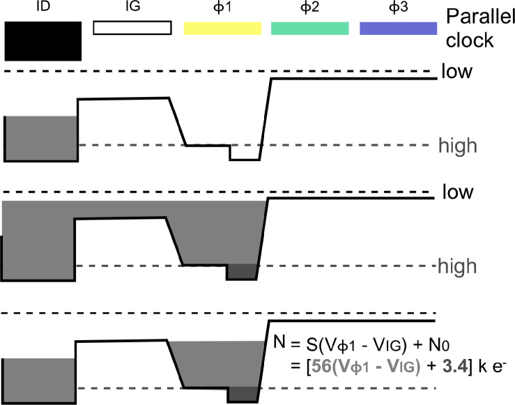
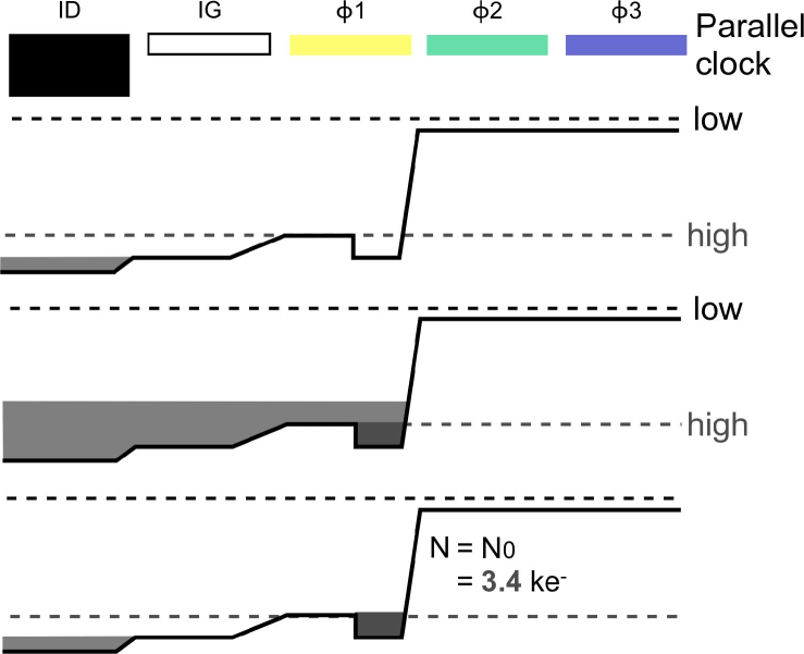
In theory MIM enables the precise injection of a very low level of charge independently of the voltage settings. The SBC FWC should be more reproducible column-to-column than using only the difference of voltage between the ‘high’ level of I1 and that on IG to inject the same small amount of charge. Without a SBC under I1, the equations in Fig 19 show that to inject 3400 requires a voltage difference of 0.06 V. Variations in oxide charge from pixel to pixel cause small fixed voltage offsets between columns at this level, which means that a single applied voltage to a single gate results in a non-uniform distribution of potential column-to-column and thus a non-uniform distribution of injected charge column-to-column. e2v expected MIM to have higher CI uniformity than VTM but this assumes only a small scatter in SBC FWCs. As explained in Section 2, SBC FWC should be uniform within a stitch block but can vary between stitch blocks. Therefore, MIM may only have higher CI uniformity than VTM within a stitch block but not necessarily over an entire CCD.
The original layout (pre-2004) of the CI structure included I1 with the nominal AL dimension of 3 m and an underlying SBC foreshortened in AL by 1 m (i.e. AL AC = 2 3 m). Burt (2005b) reports that e2v MIM testing of this structure did not find N0: the electron FWC under I1 (see Fig. 19). This was because the SBC potential was not there as its electrical size was smaller than the geometrical size due to fringing fields and manufacturing tolerances. Therefore, the CI structure was modified such that I1’s AL dimension was extended to 5 m and the SBC increased in size to 3 3 m to reduce fringing fields and increase the SBC FWC under I1 only. N0 has never been successfully detected.
References
- Burt (2003) Burt D., 2003, Technical report, AF CCD Design Report (Gaia Livelink GAIA-E2V-RP-O20)
- Burt (2005a) Burt D., 2005a, Technical report, AF CCD Design Justification (Gaia Livelink GAIA-E2V-TN-019)
- Burt (2005b) Burt D., 2005b, Technical report, Re-Design of the AF CCD (CCD91) (Gaia Livelink GAIA-E2V-RP-114)
- de Bruijne (2008) de Bruijne J., 2008, Technical report, CCD pixel pitch, stitch boundaries, and supplementary buried channel (Gaia Livelink GAIA-CH-TN-ESA-JDB-043)
- Holl et al. (2012) Holl B., Prod’homme T., Lindegren L., Brown A. G. A., 2012, MNRAS, 422, 2786
- Holland & Smith (2004) Holland A., Smith D., 2004, Technical report, Charge injection strategies for Gaia (Gaia Livelink Brunel-Gaia-TN-012)
- Hopkinson (2006) Hopkinson G., 2006, Technical report, Final Report Radiation Testing of Gaia AF and MBP CCDs (Gaia Livelink 254.DO.28)
- Hopkinson et al. (2005) Hopkinson G., Short A., Vetel C., Zayer I., Holland A., 2005, IEEE Transactions on Nuclear Science, 52, 2664
- Kohley et al. (2009) Kohley R., Raison F., Martin-Fleitas J. M., 2009, in Society of Photo-Optical Instrumentation Engineers (SPIE) Conference Series Vol. 7439 of Presented at the Society of Photo-Optical Instrumentation Engineers (SPIE) Conference, Gaia: operational aspects and tests of Gaia Flight Model CCDs
- Lindegren & Crowley (2010) Lindegren L., Crowley C., 2010, Technical report, Radiation effect on the astrometric performance of stars of G 15 (Gaia Livelink GAIA-C3-TN-LU-LL-086-01)
- Perryman et al. (2001) Perryman M. A. C., de Boer K. S., Gilmore G., Høg E., Lattanzi M. G., Lindegren L., Luri X., Mignard F., Pace O., de Zeeuw P. T., 2001, A&A, 369, 339
- Prod’homme et al. (2011) Prod’homme T., Brown A. G. A., Lindegren L., Short A. D. T., Brown S. W., 2011, MNRAS, 414, 2215
- Prod’homme et al. (2012) Prod’homme T., Holl B., Lindegren L., Brown A. G. A., 2012, MNRAS, 419, 2995
- Seabroke et al. (2010) Seabroke G., Holland A., Burt D., Robbins M., 2010, in Society of Photo-Optical Instrumentation Engineers (SPIE) Conference Series Vol. 7742 of Presented at the Society of Photo-Optical Instrumentation Engineers (SPIE) Conference, Silvaco ATLAS model of ESA’s Gaia satellite e2v CCD91-72 pixels
- Seabroke et al. (2008) Seabroke G., Holland A., Cropper M., 2008, in Dorn D. A., Holland A. D., eds, High Energy, Optical, and Infrared Detectors for Astronomy III Vol. 7021 of Proc. SPIE (Bellingham, WA, USA), Modelling radiation damage to ESA’s Gaia satellite CCDs