Fermi Velocity Modulation in Graphene by Strain Engineering
Harihar Behera***E-mail: harihar@phy.iitb.ac.in; harihar@iopb.res.in and Gautam Mukhopadhyay†††Corresponding author’s E-mail: gmukh@phy.iitb.ac.in; g.mukhopa@gmail.com
Department of Physics, Indian Institute of Technology, Powai, Mumbai-400076, India
Abstract
Using full-potential density functional theory (DFT) calculations, we found a small asymmetry in the Fermi velocity of electrons and holes in graphene. These Fermi velocity values and their average were found to decrease with increasing in-plane homogeneous biaxial strain; the variation in Fermi velocity is quadratic in strain. The results, which can be verified by Landau level spectroscopy and quantum capacitance measurements of bi-axially strained graphene, promise potential applications in graphene based straintronics and flexible electronics.
PACS: 73.22.-f, 73.63.-b, 73.22.Pr
Keywords : graphene, strain, electronic structure, Fermi velocity
1 Introduction
Graphene, a single layer of carbon atoms arranged in a two-dimensional (2D) hexagonal lattice, displays remarkable mechanical and electronic properties promising many applications in nano-devices [1]. The novel properties of graphene arise from the linear energy dispersion near the point of the hexagonal Brillouin zone (BZ):
| (1) |
where is the Fermi energy, is the Fermi velocity of electrons/holes near the point of the BZ and is the momentum. Many graphene device characteristics depend on . For instance, graphene’s fine structure constant
| (2) |
appears in the graphene device characteristics of graphene field effect transistor (GFET) [2]; for an ideal graphene with a uniform channel potential , the quantum capacitance of graphene is given by [3]:
| (3) |
where is the temperature and other symbols have their usual meanings. Thus, any change in would affect the graphene device characteristics. Although strain-induced variation in has recently been observed experimentally [4] by Raman spectroscopy study of uni-axially strained graphene, the quantitative dependence of on strain remains unclear. Here, we report our theoretical investigation on the effect of biaxial strain on the Fermi velocity of charge carriers in graphene, which is experimentally known to sustain in-plane tensile elastic strain in excess of [5]. Thus, our study mimics the experimental condition where graphene is supported on an ideal flat stretchable substrate.
2 Computational Methods
We use the DFT based full-potential (linearized) augmented plane-wave plus local orbital (FP- (L)APW+lo) method [6] as implemented in the elk code [7]. For the exchange-correlation term, we use the Perdew-Zunger variant of local density approximation (LDA) [8], the accuracy of which has been successfully tested in our previous works [9]. For plane wave expansion in the interstitial region, we have used , where is the muffintin radius, for deciding the plane wave cut-off. The -point grid size of was used for all calculations. The total energy was converged within eV/atom. The 2D hexagonal structure of graphene was simulated by 3D hexagonal super cell construction with a large value of c-parameter ( a.u.). The application of homogeneous in-plane biaxial strain was simulated by varying the in-plane lattice parameter , where is the ground state in-plane lattice constant.


3 Results and Discussions
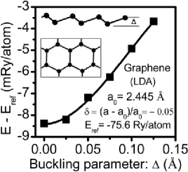
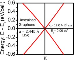
In Figure 1(a), our calculated results show that under compressive strain of graphene does not show any buckling, i.e. its planar structure remains preserved. Figure 1(b) depicts the linear energy band dispersion of unstrained graphene near the point of the BZ. In Table 1, we compare our calculated values of and with some reported values.
| (Å) | ( m/s) | Remark/Reference |
|---|---|---|
| 2.4450 | 0.8327 | This Work |
| 2.4595 | 0.833 | LAPW + GGA [10] |
| 0.79 | Experiment, graphene on graphite substrate [11] | |
| 1.093 | Experiment, graphene on SiO2/Si substrate [12] | |
| 0.81 | Experiment, single walled CNT [13] |
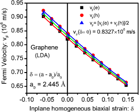
Our calculated variation of Fermi velocity of electrons , holes and their average value at different strain values are shown in Figure 2. Since values are slightly greater than values, the band structure of electrons and holes are not exactly symmetric in qualitative agreement with a recent experiment [12] and the origin of this asymmetry is not well understood [12]. The decrease in Fermi velocity with increasing strain is due to a reduction in the -orbital overlap [4]. Our calculated data in Figure 2 best fit with the following equations:
| (4) |
| (5) |
| (6) |
A possible precise measurement of the variation of with may be carried out with Landau level spectroscopy study of a bi-axially strained graphene, since the Landau level spectrum is given by [12]:
| (7) |
where is an integer, is the energy at the Dirac point, is the magnetic field perpendicular to graphene s plane and other symbols have their usual meanings. Measurement of the quantum capacitance [3] of bi-axially strained graphene can also be useful.

4 Conclusions
There exists a small asymmetry in the Fermi velocity of electrons and holes in graphene whose reason is not yet clear. The Fermi velocity in graphene can be modulated by strain engineering for potential applications in graphene based flexible electronics.
References
- [1] A. H. Castro Neto, et al., Rev. Mod. Phys. 81, 109 (2009).
- [2] F. Schwierz, Nature Nanotechnology 5, 487 (2010).
- [3] H. Xu, et al., Appl. Phys. Lett. 98, 133122 (2011).
- [4] M. Huang, et al., Nano Lett. 10, 4074 (2010).
- [5] C. Lee, et al., Science 321 (5887), 385 (2008).
- [6] E. Sjöstedt, L. Nordström, D. J. Singh, Solid State Commun. 114, 15 (2000).
-
[7]
Freely available at:
http://elk.sourceforge.net/ - [8] P. Perdew, A. Zunger, Phys. Rev. B 23, 5048 (1981).
- [9] H. Behera , G. Mukhopadhyay, J. Phys. Chem. Solids 73, 818 (2012); and other works cited in it.
- [10] M. Gmitra, et al., Phys. Rev. B 80, 235431 (2009).
- [11] G. Li, et al., Phys. Rev. Lett. 102, 176804 (2009).
- [12] K.-C. Chuang, et al., Phil. Trans. R. Soc. A 366, 237 (2008).
- [13] W. Liang, et al., Nature 411, 665 (2001).