Adsorption of Alkali, Alkaline Earth and Transition Metal Atoms on Silicene
Abstract
The adsorption characteristics of alkali, alkaline earth and transition metal adatoms on silicene, a graphene-like monolayer structure of silicon, are analyzed by means of first-principles calculations. In contrast to graphene, interaction between the metal atoms and the silicene surface is quite strong due to its highly reactive buckled hexagonal structure. In addition to structural properties, we also calculate the electronic band dispersion, net magnetic moment, charge transfer, workfunction and dipole moment of the metal adsorbed silicene sheets. Alkali metals, Li, Na and K, adsorb to hollow site without any lattice distortion. As a consequence of the significant charge transfer from alkalis to silicene metalization of silicene takes place. Trends directly related to atomic size, adsorption height, workfunction and dipole moment of the silicene/alkali adatom system are also revealed. We found that the adsorption of alkaline earth metals on silicene are entirely different from their adsorption on graphene. The adsorption of Be, Mg and Ca turns silicene into a narrow gap semiconductor. Adsorption characteristics of eight transition metals Ti, V, Cr, Mn, Fe, Co, Mo and W are also investigated. As a result of their partially occupied orbital, transition metals show diverse structural, electronic and magnetic properties. Upon the adsorption of transition metals, depending on the adatom type and atomic radius, the system can exhibit metal, half-metal and semiconducting behavior. For all metal adsorbates the direction of the charge transfer is from adsorbate to silicene, because of its high surface reactivity. Our results indicate that the reactive crystal structure of silicene provides a rich playground for functionalization at nanoscale.
pacs:
81.16.Pr, 68.65.Pq, 66.30.Pa, 81.05.ueI Introduction
Recent advances in controllable synthesis and characterization of nanoscale materials, have opened up important possibilities for the investigation of ultra-thin two-dimensional systems. Chiefly the research efforts directed towards graphenenovo ; geim have dominated the new era of two-dimensional materials. Many exceptional features of atomically thin graphene layers such as massless Dirac fermions, strength of the lattice structure, high thermal conductivity and half-integer Hall conductance have been revealed so far.kats ; novo2 ; zhang ; berger In spite of its unique properties, due to the lack of a band gap and its weak light adsorption, graphene research efforts have focused on graphene composites over the past five years. Studies have demonstrated the existence of several chemically converted graphene structures such as grapheneoxide (GO),dikin ; eda ; robinson graphane (CH),elias ; sofo ; apl2009 ; prb2010 ; graphane-m fluorographene (CF),nair ; robinson2 ; withers ; leenaerts ; hasancf and chlorographene (CCl).cl-exp ; hasan-cl ; mari-cl High- quality insulating behavior, thermal stability and extraordinary mechanical strength of fluorographene (CF) has inspired intense research on halogenated graphene derivatives.
Unusual properties of graphene promising for a variety of novel applicationsc-ads ; coating ; mesh ; sefa1 ; sefa2 ; sefa3 have also triggered significant interest in one or several atom-thick honeycomb structures of binary compounds. Early experimental studies aiming to synthesize and characterize novel monolayer materials have revealed that graphene-like sheets of BN are also stable.bn-synthesis ; bn-prl ; bn-nature Though BN has the same planar structure as graphene due to the ionic character of B-N bonds, BN crystal is a wide band gap insulator with an energy gap of 4.6 eV.Guo ; louie-nanoletter ; barone2 ; bn-mehmet The perfect lattice matching between graphene and BN layers make it possible to construct nanoscale devices. novoselov-nobel Following the synthesis of hexagonal monolayer of ZnO,znobilayer the II-VI metal-oxide analogue of graphene, it was also predicted that ZnO nanoribbons have ferromagnetic order in their ground state.mendez1 In addition to these, it was reported that common solvents can be used to exfoliate transition metal dichalcogenides and oxides such as MoS2, WS2, MoSe2, MoTe2, TaSe2, NbSe2, NiTe2, Bi2Te3 and NbSe2 to obtain single layers.Coleman ; mos2 ; ws2 ; pnas Most recently, possibility of various combinations of MX2 type single-layer transition-metal oxides and dichalcogenides, stable even in free-standing form, was also predicted.mx2miz
The recent synthesis of silicene,silicene-exp1 ; silicene-exp2 ; silicene-exp3 the silicon analogue of graphene has opened a new avenue to nanoscale material research. Though the nanotubesint and fullerenesiful forms of silicon were synthesized earlier, monolayer silicon was presumed not to exist in a freestanding form. Early theoretical works pointed out that silicene is a semimetal with linearly crossing bands and it has a buckled crystal structure that stems from hybridization.seymur ; hasan Similar to graphene, the hexagonal lattice symmetry of silicene exhibits a pair of inequivalent valleys in the vicinity of the vertices of and symmetry points. Moreover, the experimental realization of the transformation of thin films of wurtzite (WZ) materials into the graphene-like thin film structure is another evidence for the existence of monolayer structures of Si and Ge.stabilizing Recent theoretical studies have revealed several remarkable features of silicene such as a large spin-orbit gap at the Dirac point,silicene-soc experimentally accessible quantum spin Hall effect,silicene-qshe transition from a topological insulating phase to a band insulator that can be induced by an electric fieldsilicene-ti and electrically tunable band gap.silicene-falko In addition to unique insulator phases such as quantum spin Hall, quantum anomalous Hall and band insulator phases, the emergence of valley-polarized metal phase was also reported very recently.motohiko It appears that silicene will be a possible graphene replacement not only due to its graphene-like features but also because of its compatibility to existing silicon-based electronic devices.
In this paper, motivated by the very recent experimental realizations of monolayer silicene,silicene-exp1 ; silicene-exp2 ; silicene-exp3 we investigate how alkali, alkaline earth, and transition metal atoms interact with monolayer freestanding silicene. Details of computational methodology are described in Sec. II. Characteristic properties of monolayer silicene and graphene are compared briefly. Our results on structural and electronic properties of metal adatom adsorbed silicene are presented in Sec. IV. Conclusions and a summary of our results are given in Sec. V.
II Computational Methodology
To investigate the adsorption characteristics of alkali metals and transition metals on a monolayer honeycomb structure of silicone we employ first-principles calculationskresse using the projector augmented wave (PAW) methodpaw implemented in VASP code. Electronic exchange-correlation effects are simulated using the spin polarized local density approximationlda (LDA). For the plane-wave basis set, the kinetic energy cutoff is taken to be eV. Brillouin zone (BZ) sampling is determined after extensive convergence analysis. In the self-consistent potential, total energy and binding energy calculations with a (661) supercell of silicene sheet a set of (551) k-point sampling is used for BZ integration. For partial occupancies the Gaussian smearing method is used. The convergence criterion of our self consistent calculations for ionic relaxations is eV between two consecutive steps. By using the conjugate gradient method, all atomic positions and the size of the unitcell were optimized until the atomic forces were less than 0.05 eV/Å. Pressures on the lattice unit cell are decreased to values less than 1 kB. Adatom adsorbed silicene monolayers are treated using a supercell geometry, where a minimum of 15 Å vacuum spacing is kept between the adjacent silicene layers. Diffusion pathway of adatoms are calculated for 10 different adsorption points on (441) silicene supercell.
| Material | Å | Å | Å | rad | ||||
|---|---|---|---|---|---|---|---|---|
| Graphene | 2.46 | 1.42 | - | 120 | 4.49 | 17.87 | 335hasancf | 900-1600 |
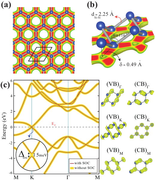
| Silicene | 3.83 | 2.25 | 0.49 | 116 | 4.77 | 9.07 | 63strain | 150-580hasan |
The cohesive energy of silicene (also for graphene) per unit cell relative to free Si atom, given in Table 1, is obtained from , where is the total energy of single free Si and is the total energy of silicene. Here total energy of single atoms are calculated by considering their magnetic ground state. As for the adsorption energy of a metal adatom, one can use the formula where , and are the total energies of (661) supercell of silicene, isolated single adatom and silicene+adatom system, respectively.
Most of the adatom adsorption result in a net electrical-dipole moment perpendicular to the plane. Therefore ground state electronic structure, magnetic state and workfunction are calculated by applying a dipole correctiondipole to eliminate the artificial electrostatic field between the periodic supercells. To obtain continuous density of states curves and to determine the energy bandgap () smearing with 0.2 and 0.001 eV is used, respectively. For the charge transfer analysis, the effective charge on the atoms are obtained by the Bader method.bader
III Silicene
Though crystalline silicon has the diamond structure and no layered form exists in nature, very recent experimental studies have reported the successful synthesis of a monolayer of silicon, called silicene, by the application of various deposition techniques. Similar to graphene, silicene can be viewed as a bipartite lattice composed of two inter-penetrating triangular sublattices of silicon atoms. Since bonds between silicon atoms are weaker than in the case of the carbon atoms, planarity is destabilized and therefore silicone atoms are buckled in a silicene crystal. As shown in Fig. 1(b) the buckling (perpendicular distance between these two Si planes) is 0.49 Å. Upon the formation of bonded honeycomb lattice, the covalent bond length of Si-Si is 2.25 Å.
Two dimensional silicene sheet is a semimetal because the valence and conduction bands touch at the Fermi level. It was predicted earlier that similar to graphene, silicene has also linearly crossing bands at the (and ) symmetry points and charge carriers in graphene behave like relativistic particles with a conical energy spectrum with Fermi velocity like in graphene.seymur ; hasan In Fig. 1(c), the electronic band structure of perfect silicene is presented. Linear and bands that cross at the symmetry point are responsible for the existence of massless Dirac fermions in silicene. Due to the degeneracy of the valence band (VB) maxima and the conduction band (CB) minima at the point, corresponding states have the same ionization potential and electron affinity. Therefore one can expect the observation of similar unique properties of graphene in silicene. The calculated energy band gaps at and symmetry points are 1.64 and 3.29 eV, respectively. At the point, the degenerate VB is composed of and orbitals, while the CB is formed by the hybridization of and orbitals.
In Fig.1(c) we also present the electronic band dispersion taking into account spin-orbit coupling (SOC). Though clearly the inclusion of spin-orbit interaction does not result in a visible change in band dispersion, a band gap of meV appears at the K point. Due to its buckled structure, silicene has a larger SO-induced gap than graphene which is of the order of 10-3 meV.soc-gr The calculated band structure and band gap opening () with SOC is in good agreement with recently reported studies.silicene-qshe ; silicene-soc ; motohiko
In Table 1 we also compare structural, electronic and vibrational properties of graphene and silicene. It appears that in contrast to the general trend that the larger the atomic radius, the smaller the workfunction, silicene’s workfunction is 4.77 eV, while for graphene it is 4.49 eV. The calculated values of in plane stiffnessstrain and cohesive energy indicates that silicene is a stable but less stiffer material as compared to graphene. Similar to graphene’s out-of-plane optical (ZO) phonon mode at 900 , silicene has a ZO mode at 150 . Eigenfrequency of the LO and TO modes are degenerate at the symmetry point are found to be 580 which is almost three times smaller than graphene’s LO (and TO) modes.
IV Results: Adsorption of Metal Atoms
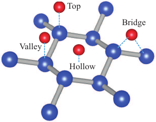
As shown in Fig. 2, regarding the interaction of silicene surface with adsorbates four different adsorption positions can be considered i.e., above the center of hexagonal silicon rings (Hollow site), on top of the upper silicon atoms (Top-site), on top of the lower silicon atoms (Valley-site), on top of the Si-Si bond (Bridge site). Considering the monolayer hexagonal lattice structure of silicene, it is reasonable to expect the relaxation of foreign atoms to one of these adsorption sites.
IV.1 Bonding Geometry and Migration Barriers
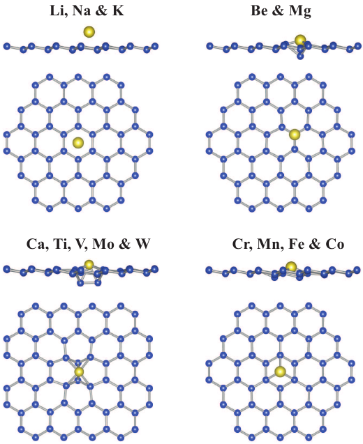
We first investigate the adsorption characteristics of alkali adatoms Li, Na and K on silicene. The alkali metals are highly reactive metals and their chemical activity increases from Li to Fr. Characteristic bonding geometry of alkali atoms are depicted in Fig.3. Upon full geometry optimization, all alkali atoms Li, Na and K atoms favors bonding on the hollow site of the silicene layer. Adsorption of alkali atoms does not yield any significant distortion or stress on the silicene lattice. The valley site on the low-lying silicon atoms is the next favorable site. Though the top and valley site adsorptions are also possible, bridge site adsorption of alkalis is not possible on a silicene lattice. Therefore the bridge site adsorption is a kind of transition state between top and valley sites. Structural and electronic properties of alkali metals adsorbed on silicene layer are also presented in Table 2. Here the height of adatoms is calculated as the difference between the average coordinates of neighboring Si atoms and the adsorbate. The distance between the adatom and silicene surface monotonically increases with increasing atomic size. However, fully conforming to graphene,chan there is no clear trend in the adsorption energies. While adsorption energies of Li, Na and K on graphene were calculated to be 1.1, 0.5 and 0.8 eV, respectively, their binding to silicene lattice is more than twice stronger, i.e. 2.4, 1.9 and 2.1 eV, respectively. The nature of the alkali-silicene bond will be discussed in the next subsection.
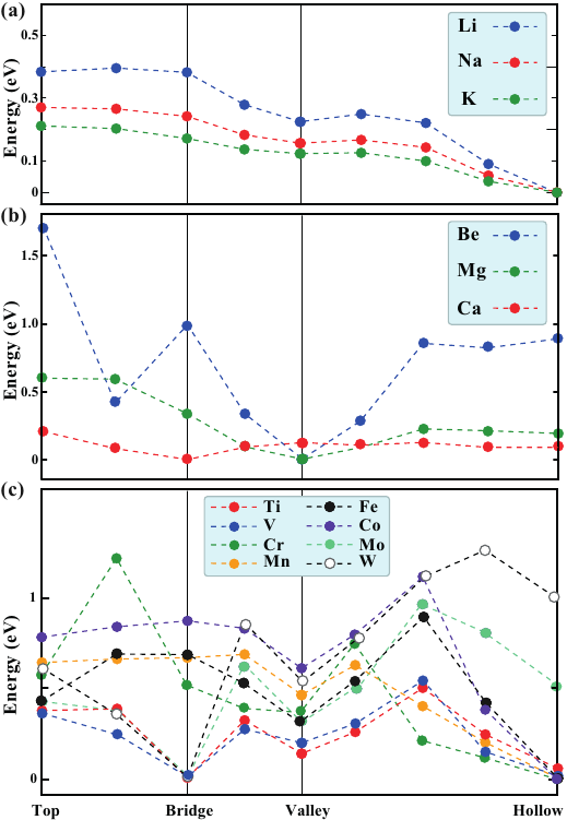
Possible diffusion pathways of the adsorbate atoms on silicene lattice can also be deduced from the energy barrier between hollow, valley, top and bridge sites. In Fig. 4 we present the energetics of different adsorption sites. For alkali atoms, shown in Fig. 4(a) it appears that the most likely migration path between subsequent hollow sites passes thorough the nearest valley sites. It is also seen that the energy difference between hollow and valley sites becomes smaller for larger atoms and therefore the diffusion of larger alkali atoms are relatively easier. Though alkali atoms strongly bind to the silicene surface, at high temperatures they may diffuse along hollow and valley sites when they overcome the energy barrier of 140-280 meV.
Alkaline earth metals are the elements of the periodic table having two valence electrons in their outermost orbital. Compared to alkalis, alkaline earth metals have smaller atomic size, higher melting point, higher ionization energy and larger effective charge. Strong interaction between alkaline earths and silicon surfaces is well-known and have been used for various silicon etching and surface engineering techniques. Therefore one can expect strong bonding of alkaline earth’s to a monolayer silicon surface. Resulting atomic geometries for Be, Mg and Ca adsorbed on a silicene sheet are depicted in Fig. 3. Unlike alkalis, the hollow site is not the most favorable adsorption site for alkaline earth metals. Among these, while Be and Mg favor adsorption to a valley site, the Ca adsorbate that has a quite large atomic size (empirically 1.8 Å) prefers bridge site adsorption. Adsorption energy of alkaline earth’s is slightly higher for alkali metals (except Mg). Similar to the Na adsorbate a second row element, adsorption energy has a sharp decrease for the second row alkali element Mg. As shown in Fig. 4(b), the Be atom has to overcome a quite large energy barrier (E > 1 eV) for migration from valley to other adsorption sites. Sudden increases in migration barrier stem from the stretching of silicene lattice by adsorbate which is freed only in one direction perpendicular to the surface. At high temperatures, migration of Ca atoms through bridge and hollow sites may take place by overcoming the energy barrier of 125 meV.
| Site | p | ||||||||
|---|---|---|---|---|---|---|---|---|---|
| (Å) | () | () | (Å) | () | () | ||||
| Li | H | 1.69 | 2.40 | 1.0 | 0.0 | m | 0.30 | 0.8 | 4.39 |
| Na | H | 2.19 | 1.85 | 1.0 | 0.0 | m | 0.60 | 0.8 | 4.25 |
| K | H | 2.70 | 2.11 | 1.0 | 0.0 | m | 0.94 | 0.8 | 4.09 |
| Be | V | 0.78 | 2.87 | 0.0 | 0.0 | 0.39 | 0.00 | 1.3 | 4.68 |
| Mg | V | 1.98 | 1.22 | 0.0 | 0.0 | 0.48 | 0.31 | 1.0 | 4.81 |
| Ca | B | 1.49 | 2.68 | 0.0 | 0.0 | 0.17 | 0.62 | 1.3 | 4.47 |
| Ti | B | 0.77 | 4.89 | 4.0 | 2.0 | hm | 0.29 | 0.9 | 4.77 |
| V | B | 0.62 | 4.32 | 5.0 | 2.7 | 0.06 | 0.18 | 0.7 | 4.84 |
| Cr | H | 0.48 | 3.20 | 6.0 | 4.0 | hm | 0.12 | 0.3 | 4.65 |
| Mn | H | 1.04 | 3.48 | 5.0 | 3.0 | 0.24 | 0.10 | 0.4 | 4.73 |
| Fe | H | 0.33 | 4.79 | 4.0 | 2.0 | 0.18 | 0.00 | 0.0 | 4.81 |
| Co | H | 0.72 | 5.61 | 3.0 | 1.0 | m | 0.00 | 0.0 | 5.00 |
| Mo | B | 0.37 | 5.46 | 6.0 | 0.0 | m | 0.15 | 0.1 | 4.97 |
| W | B | 0.01 | 7.05 | 6.0 | 0.0 | 0.02 | 0.04 | 0.2 | 4.90 |
We next investigate the adsorption characteristics of eight elements of the , and transition metal adatoms: Ti, V, Cr, Mn, Fe, Co, Mo and W. Though the outermost orbitals of the transition metals are completely filled, because of their partially filled inner orbitals diverse adsorption characteristics for different atoms can be expected. Due to relatively small atomic radius of all transition metals and having more electrons that can participate in the chemical bonding, we can expect stronger binding to the silicene lattice. From Fig. 3 it appears that while the adsorption of alkalis do not cause any significant change in the silicene lattice, transition metals are more likely to disturb the nearest silicon atoms.
Bonding of Ti adatom with 4.89 eV to silicene occurs with a significant lattice distortion whereas the adsorption of Ti occurs on the hollow site of graphene without disturbing the planar lattice structure. As a consequence of bridge-site adsorption of Ti, it binds six nearest Si atoms strongly by pushing the underlying two Si atoms downwards. In order not to exclude possible vacancy formation and adatom-induced fracturing in such Ti-adsorbed silicene lattice we also examine the stability of whole structure through molecular dynamics (MD) calculations. Ab initio MD calculations show that the adsorbed Ti atom remains bounded and neighboring Si-Si bonds are not broken after 1 at 300 K. Similar to Ti, V adatom is adsorbed on bridge site with 4.32 eV adsorption energy.
Among the transition metal adatoms considered here only Cr, Mn, Fe and Co similar to alkalis, are adsorbed on the hollow site. However, differing from alkalis, transition metals have quite strong binding (3.20, 3.48, 4.79 and 5.61 for Cr, Mn, Fe and Co, respectively) with three uppermost Si atoms. Therefore, instead of being adsorbed on top a hollow site like alkalis, transition metals are almost confined in the silicene plane. Energetics of transition metal atoms on the most favorable adsorption sites are also listed in Table 2.
Note that not only the electronic occupancy but also the atomic radius of the atom is important in determining the final geometry of the adatom on silicene. Since for orbitals having more than half-occupancy the atomic radii are significantly decreased by increasing the number of electrons, starting from Cr all 3 transition metals prefer to be relaxed on hollow site. To see how the atomic radius of transition metal affects the adsorption geometry we also perform calculations for other Group 6 elements Mo and W. According to the most recent measurement of Cordero et al.radius covalent atomic radii of Cr, Mn and W are 1.39, 1.54 and 1.62 Å, respectively. In this column of the Periodic Table, while Cr is adsorbed on hollow site, bridge site adsorption becomes more preferable for Mo and W due to their larger atomic radii. Effect of the atomic radii can also be seen even in the same row elements: adatoms Ti and V, that have covalent radius larger than that of Cr, are relaxed to the bridge site. Thus we can infer that only the transition metal adatoms having covalent atomic radii larger than 1.50 Å favor bridge site adsorption.
It appears from Fig. 4(c) that the energy barrier between different adsorption sites is relatively large for transition metal atoms. The diffusion barrier between the most favorable site and the less favorable one is 0.6 eV. The most likely diffusion path for Ti, V, Mo and W passes from bridge to hollow sites. However, diffusion of Mn, Cr, Fe and Co atoms from one hollow site to another one may occur via valley sites.
Furthermore, the effect of spin-orbit interaction on the optimized adsorbate-silicene geometry is examined for adsorption on (661) silicene supercell. Compared with the optimized geometries obtained excluding SOC, SO-induced change in adatom-silicon bond length is just on the order of 0.001 Å. It is also found that the migration path profile and the most favorable adsorption site do not change when SOC is included. Therefore, due to negligible effect of spin-orbit interaction on structural properties, in the rest of our study LDA calculations will be employed.
IV.2 Electronic Structure
In this section we present spin-polarized electronic band dispersion and density of states (DOS) for adatoms adsorbed on the most favorable site on the silicene surface. Since the alkaline earth and transition metal adsorption significantly disturb the hexagonal lattice symmetry, electronic band dispersion along the high symmetry points (-M-K-) of perfect silicene may not represent the real electronic properties of the whole structure. Therefore, a density of states plot covering large number of k-points in the BZ is more convenient for a reliable description of the electronic structure.
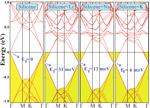
In Fig. 5, we present electronic band dispersions of alkali metal adsorbed silicene. For the sake of comparison, the band structure of the bare silicene is also included. Here it is worth to note that the Dirac cone that is located at 2/3 of first BZ is shifted from to high symmetry point due to band folding of the (661) silicene supercell. Similar shift can be obtained by band folding operations for all (3n3n1) supercells (=1, 2,…). As a result of the adsorption of an alkali atom, semimetallic silicene becomes metallic due to the donation of 0.8 e charge from the alkali atom into the silicene conduction band. Such an attraction of adatom through the hollow site of the silicene surface with a significant charge transfer resembles ionic bonding. Moreover, since the band dispersion of perfect silicene is negligibly disturbed by the alkali adatoms, it seems reasonable to assume that the bonding is of ionic type. Here, in accordance to the charge transfer, the Fermi level (EF) is shifted by 0.2 eV. It is seen that all alkali atom adsorption bands formed by the hybridization of adsorbate- states with the silicene- states appear in the vicinity of 0.4 eV. Additionally, a small gap opening in the bands below the Fermi level, which is 6, 13 and 31 meV for Li, Na and K, respectively, occur at the crossing point.
While each isolated alkali atom has a net initial magnetic moment of 1 , up-down spin degeneracy is not broken upon 0.8 charge transfer and therefore all the silicene+alkali structures are nonmagnetic metals. However, as a result of the large charge transfer between the alkali atom and silicene, remarkable dipole moment perpendicular to the silicene surface is induced. Calculated value of the dipole moment directed from silicene to the adatom is 0.30, 0.60 and 0.94 eÅ for Li, Na and K, respectively. Though the amount of the charge transfered is almost the same for all alkalis, the induced dipole moment is different due to the difference in distance between the adsorbate and the silicene layer. As a consequence of adatom-induced surface charge density redistribution, the workfunction of the silicene surface is decreased. Therefore, the trend of the increase in the dipole moment follows the decrease in workfunction.
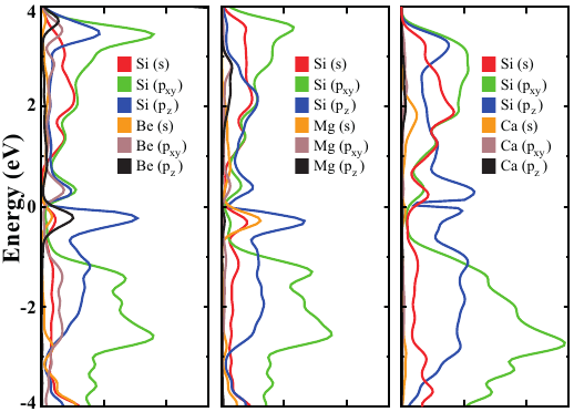
Alkaline earth metals are highly reactive elements that tend to form various compounds by loosing two outermost shell electrons. Natural silicate and carbonate forms of alkaline earths are well-known. As shown in Table 2, Be, Mg and Ca adsorption yields a gap opening of 0.39, 0.48 and 0.17 eV, respectively. It is also seen from the partial density of states shown in Fig. 6 that the top of the valence band (VB) of Be adsorbed silicene is due to the hybridization of and orbitals of the nearest silicon atoms and the alkaline earth metals. However, at top of the VB main contribution comes from Mg-, Si- and Si- hybridization, whereas orbital of Mg does not mix with surrounding silicon states. The bottom of the conduction band (CB) of both Be and Mg is formed by hybridization of states of adsorbates with and states of silicene. Differing from Be and Mg, adsorption of Ca on silicene does not yield appearance of Ca states around EF. While the states at the VB edge arise mainly from the silicene orbitals, the CB edge is composed of , and orbitals of Si.
Since atomic states of transition metal atoms have comparable energy values to that of their valence states, the shell of these atoms is partially filled. The net magnetic moment of isolated transition metals are nonzero and behave like small magnets unless the shell is completely filled. Though the shell electrons are located close to the nucleus like the characteristic core electrons, they can spread out much further like valence electrons. Therefore, transition metals with their partially filled shells are relaxed to different sites on silicene and we can expect diverse electronic properties upon their adsorption. We depict the spin-polarized electronic density of states of those transition metal adsorbed silicene in Fig 7.
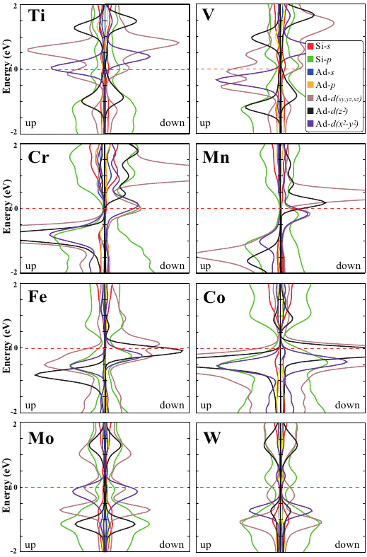
Ti adsorption on silicene has a quite different characteristics as compared to other transition metals. Upon the adsorption of a Ti atom that has an initial magnetic moment of 4.0 in its isolated state, on bridge site of silicene the structure becomes a ferromagnetic metal with 2.0 net magnetic moment per supercell. Since we use a quite large supercell such that the adatom-adatom interactions are negligible, describing the adatom levels in terms of orbitals, instead of bands, is more appropriate. As a result of the strong bonding, the silicene lattice is significantly distorted, Ti atom binds to six nearest Si atoms and the degeneracies of the Ti- states are completely broken. Metallic bands of the structure originates only from the Ti-() orbitals and silicene becomes half metal when Ti adatom is adsorbed.
For the case of V adsorption on silicene, the structure becomes semiconductor with 2.7 net magnetic moment per supercell. It is seen from Fig 7 that while only V-() states have a significant contribution to VB maximum, bottom of the CB is derived from Si-() and V-(). The contribution of the other eigenstates at the vicinity of EF are enhanced just because of the smearing of the DOS plot. Cr adsorption also turns the semimetallic silicene into a half metallic material with 4 per supercell. The up spin (minority) bands of the Cr adsorbed silicene are semiconducting with a direct band gap of 0.4 eV, whereas the down spin (majority) band shows metallic behavior. The bands in the vicinity of EF are mainly derived from the hybridization of Cr-() and Cr-() orbitals and the Si-() states. However, differing from Cr, the adsorption of Mo and W that occurs on bridge site results in a nonmagnetic ground state. While Mo-adsorbed silicene becomes metallic due to Mo- states at EF, W-adsorbed silicene is a nonmagnetic semiconductor with bandgap of 0.02 eV. Note that the half-metallic behavior for Ti- and Cr-decorated silicene can be quite important for potential use in spintronics.
The adsorption of Mn atom in close proximity to the hollow site of buckled hexagonal lattice results in semiconducting behavior with a bandgap of 0.24 eV. The degeneracy of and spin states are broken due to the existence of a net magnetic moment of 3.0 . Since Mn, Fe and Co atoms have the smallest atomic size of the considered metal atoms here, they are the most closely bonded one among all hollow site adsorbed atoms. Both the adsorption of Fe and Co result in metallic ground state, that originates from the () and () states at EF, with 2 and 1 net magnetic moment, respectively. As a consequence of the small adsorption height, the induced dipole moments are much smaller than those of the alkali adatom adsorbed silicene.
The adsorbate-induced magnetic moments induced in the silicene layer lead to an exchange-splitting especially in eigenstates. The calculated value of the exchange-splitting is 0.4, 2.0, 2.1, 1.9, 0.5 and 0.4 eV for Ti, V, Cr, Mn, Fe and Co, respectively. However, bridge-site adsorbed Mo and W adatoms exhibits no splitting due to their nonmagnetic ground state.
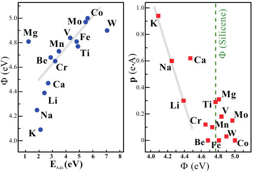
To reveal the correlations between adsorption energy (EAds), workfunction () and induced dipole moment (p) we also present -EAds and p- plots as shown in Fig 8. Note that the adsorption of large transition metals that occurs with large binding energy changes the silicene’s workfunction negligibly. Especially for transition metals having more than half filled -subshell, the larger the adsorption energy the higher the workfunction. However, it appears that even with a small coverage (1/72) of silicene surface by alkali metals, a significant decrease of the work function can be produced. For alkalis and alkaline earths, there is almost a linear correlation between EAds and . Because of the ionic nature of the alkali-silicene bonding, the workfunction linearly depends on the atomic size and therefore one can expect a significant decrease (>1 eV) in the workfunction for adsorption of larger alkalis on silicene. It is also seen that, while multivalent adatoms do not follow a particular trend in dipole moment, for alkali atoms workfunction shift exhibits a linear decrease with increasing dipole moment.
V Conclusions
In this study, we presented a first-principles investigation of the adsorption characteristics of alkali (Li, Na and K), alkaline earth (Be, Mg and Ca) and transition metals (Ti, V, Cr, Mn, Fe, Co, Mo and W) on silicene. Investigation of the interaction of silicene with metal atoms has a significant importance because of its fundamental relevance to applications in catalysis, batteries and nanoelectronics.
We found that silicene has quite different adsorption characteristics as compared to grapheneweh1 ; weh2 because of the diversity of adsorption geometries and its high surface reactivity. As a consequence of its buckled lattice structure, all the metal atoms bind strongly to silicene. While the binding energy of alkali and alkaline earth metals is 1-3 eV, transition metals have larger binding energies of 3-7 eV. Our diffusion path analysis shows that compared to graphene migration of metal atoms on a silicene lattice is more difficult and requires to overcome higher energy barriers. On the other hand, diffusion of metal atoms Li, Na, K, Mg and Ca may occur at moderate temperatures. Depending on the adatom type, semimetallic silicene can show metal, half-metal and semiconducting behavior. It was also noted that as a result of the high surface reactivity the direction of the charge transfer is always from metal adsorbate to silicene. However, the existence of charge donation and the resulting adatom-induced dipole modify the workfunction of silicene considerably. Especially the linear decrease in for larger alkali adatoms is promising for tunable enhancement of electron and ion emission which is appealing to silicene-based thermionic converters and cathodes. Our findings also suggest that the half-metallic ferromagnetic nature of Ti- and Cr-decorated silicene have a great potential for silicon-based spintronic device applications. Moreover the existence of a tunable bandgap opening in silicene by alkaline earth metal adatoms is highly desirable for its use in nanoscale optoelectronic device applications.
The extension of our investigation to a detailed study to include the effect of spin-orbit coupling and of the substrate interactions on the adsorption characteristics of silicene is planned for future studies.
VI Acknowledgements
This work was supported by the Flemish Science Foundation (FWO-Vl). Computational resources were provided by TUBITAK ULAKBIM, High Performance and Grid Computing Center (TR-Grid e-Infrastructure). H. S. is supported by a FWO Pegasus Marie Curie Fellowship.
References
- (1) K. S. Novoselov, A. K. Geim, S. V. Morozov, D. Jiang, S. C. Dubonos, I. V. Grigorieva, and A. A. Firsov, Science 306, 666 (2004).
- (2) A. K. Geim, and K. S. Novoselov, Nature Materials 6, 183 (2007).
- (3) M. I. Katsnelson, K. S. Novoselov, and A. K. Geim, Nat. Phys. 2, 620 (2006).
- (4) K. S. Novoselov, A. K. Geim, S. V. Morozov, D. Jiang, M. I. Katsnelson, I. V. Grigorieva, S. V. Dubonos, and A. A. Firsov, Nature (London) 438, 197 (2005).
- (5) C. Berger, Z. Song, T. Li, X. Li, A. Y.Ogbazghi, R. Feng, Z. Dai, A. N. Marchenkov, E. H. Conrad, P. N. First, and W. A. de Heer, Science 312, 1191 (2006).
- (6) Y. Zhang, Yan-Wen Tan, H. L. Stormer, and P. Kim, Nature (London) 438, 201 (2005).
- (7) D. A. Dikin, S. Stankovich, E. J. Zimney, R. D. Piner, G. H. B. Dommett, G. Evmenenko, S. T. Nguyen, and R. S. Ruoff, Nature (London) 448, 457 (2007).
- (8) G. Eda, G. Fanchini and M. Chhowalla, Nature Nanotech. 3, 270 (2008).
- (9) J. T. Robinson, F. K. Perkins, E. S. Snow, Z. Wei and P. E. Sheehan, Nano Lett. 8, 3137 (2008).
- (10) D. C. Elias, R. R. Nair, T. M. G. Mohiuddin, S. V. Morozov, P. Blake, M. P. Halsall, A. C. Ferrari, D. W. Boukhvalov, M. I. Katsnelson, A. K. Geim, and K. S. Novoselov, Science 323, 610 (2009).
- (11) J. O. Sofo, A. S. Chaudhari and G. D. Barber,Phys. Rev. B 75, 153401 (2007).
- (12) H. Sahin, C. Ataca and S. Ciraci, Appl. Phys. Lett. 95, 222510 (2009).
- (13) H. Sahin, C. Ataca and S. Ciraci, Phys. Rev. B 81, 205417 (2010).
- (14) M. Topsakal, S. Cahangirov, and S. Ciraci, Appl. Phys. Lett. 96, 091912 (2010).
- (15) R. R. Nair et al., Small 6, 2877 (2010).
- (16) J. T. Robinson, J. S. Burgess, C. E. Junkermeier, S. C. Badescu, T. L. Reinecke, F. K. Perkins, M. K. Zalalutdniov, J. W. Baldwin, J. C. Culbertson, P. E. Sheehan, and E. S. Snow, Nano Lett. 10, 3001 (2010).
- (17) F. Withers, M. Dubois, and A. K. Savchenko, Phys. Rev. B 82, 073403 (2010).
- (18) O. Leenaerts, H. Peelaers, A. D. Hernandez-Nieves, B. Partoens, and F. M. Peeters, Phys. Rev. B 82, 195436 (2010).
- (19) H. Sahin, M. Topsakal, and S. Ciraci, Phys. Rev. B 83, 115432 (2011).
- (20) B. Li, L. Zhou , D. Wu, H. Peng , K. Yan , Y. Zhou and Z. Liu, ACS Nano. 5, 5957 (2011).
- (21) H. Sahin and S. Ciraci, J. Phys. Chem. C, 116 (45), 24075 (2012).
- (22) M. Ijas, P. Havu, and A. Harju, Phys. Rev. B 85, 035440 (2012).
- (23) C. Ataca, E. Akturk, H. Sahin, and S. Ciraci, J. Appl. Phys. 109, 013704 (2011).
- (24) M. Topsakal, H. Sahin, and S. Ciraci, Phys. Rev B 85, 155445 (2012).
- (25) H. Sahin and S. Ciraci, Phys. Rev. B 84, 035452 (2011).
- (26) X. Miao, S. Tongay, M. K. Petterson, K. Berke, A. G. Rinzler, B. R. Appleton, A. F. Hebard, Nano Lett., 12 (6), 2745 (2012).
- (27) S. Tongay, M. Lemaitre, X. Miao, B. Gila, B. R. Appleton, and A. F. Hebard, Phys. Rev. X 2, 011002 (2012).
- (28) S. Tongay, M. Lemaitre, T. Schumann, K. Berke, B. R. Appleton, B. Gila, and A. F. Hebard, Appl. Phys. Lett. 99, 102102 (2011).
- (29) K. S. Novoselov, D. Jiang, F. Schedin, T. Booth , V. V. Khotkevich, S. Morozov, A. K. Geim, Proc. Natl. Acad. Sci. U.S.A. 102, 10451 (2005)
- (30) C. Jin, F. Lin, K. Suenaga, and S. Iijima, Phys. Rev. Lett. 102, 195505 (2009).
- (31) L. Ci, L. Song, C. Jin, D. Jariwala, D. Wu, Y. Li, A. Srivastava, Z. F. Wang, K. Storr, L. Balicas, F. Liu and P. M. Ajayan, Nature Materials 9, 430 (2010).
- (32) Z. Zhang and W. Guo, Phys. Rev. B 77, 075403 (2008).
- (33) Cheol-Hwan Park and Steven G. Louie, Nano Lett. 8, 2200 (2008).
- (34) V. Barone, J. E. Peralta, Nano Lett. 8, 2210 (2008).
- (35) M. Topsakal, E. Akturk, and S. Ciraci, Phys. Rev. B 79, 115442 (2009).
- (36) K. S. Novoselov, Ang. Chem. Int. Ed. 50, 6986 (2011).
- (37) C. Tusche, H. L. Meyerheim and J. Kirschner, Phys. Rev. Lett. 99, 026102 (2007).
- (38) A. R. Botello-Mendez, F. Lopez-Urias, M. Terrones, H. Terrones, Nano Letters 6, 1562 (2008).
- (39) J. N. Coleman et al., Science 331, 568 (2011).
- (40) K. F. Mak, C. Lee, J. Hone, J. Shan, T. F. Heinz, Phys. Rev. Lett. 105, 136805 (2010).
- (41) Z. Wang, K. Zhao, H. Li, Z. Liu, Z. Shi, J. Lu, K. Suenaga, S. Joung, T. Okazaki, Z. Jin, Z. Gu, Z. Gao, and S. Iilima, J. Mater. Chem. 21, 171 (2011).
- (42) K. S. Novoselov, D. Jiang, F. Schedin, T. J. Booth, V. V. Khotkevich, S. V. Morozov, and A. K. Geim, Proc. Natl. Acad. Scie. USA 102, 10451 (2005).
- (43) C. Ataca, H. Sahin and S. Ciraci, J. Phys. Chem. C, 116, 8983 (2012).
- (44) P. De Padova, C. Quaresima, C. Ottaviani, P. M. Sheverdyaeva, P. Moras, C. Carbone, D. Topwal, B. Olivieri, A. Kara, H. Oughaddou, B. Aufray, and G. Le Lay, Appl. Phys. Lett. 96, 261905 (2010).
- (45) P. De Padova, C. Quaresima, P. Perfetti, B. Olivieri, B. Leandri, B. Aufray, S. Vizzini, and G. Le Lay, Nano Lett. 8, 271 (2008).
- (46) P. Vogt, P. De Padova, C. Quaresima, J. Avila, E. Frantzeskakis, M. C. Asensio, A. Resta, B. Ealet, and G. Le Lay, Phys. Rev. Lett. 108, 155501 (2012).
- (47) D. F. Perepichka and F. Rosei, Small 2 (2006).
- (48) B. Marsen and K. Sattler, Phys. Rev. B 60, 11593 (1999).
- (49) S. Cahangirov, M. Topsakal, E. Aktürk, H. Sahin, and S. Ciraci, Phys. Rev. Lett. 102, 236804 (2009).
- (50) H. Sahin, S. Cahangirov, M. Topsakal, E. Bekaroglu, E. Aktürk, R. T. Senger, and S. Ciraci, Phys. Rev. B 80, 155453 (2009).
- (51) D. Wu, M. G. Lagally, and F. Liu, Phys. Rev. Lett. 99 026102 (2007).
- (52) Cheng-Cheng Liu, H. Jiang, and Y. Yao, Phys. Rev. B 84, 195430 (2011)
- (53) Cheng-Cheng Liu, W. Feng, and Y. Yao, Phys. Rev. Lett. 107, 076802 (2011)
- (54) M. Ezawa, New J. Phys. 14 033003 (2012).
- (55) N. D. Drummond, V. Zolyomi, and V. I. Fal’ko Phys. Rev. B 85, 075423 (2012)
- (56) M. Ezawa, Phys. Rev. Lett. 109, 055502 (2012).
- (57) G. Kresse and J. Hafner, Phys. Rev. B 47, 558 (1993); G. Kresse and J. Furthmüller, Phys. Rev. B 54, 11169 (1996).
- (58) P. E. Blochl, Phys. Rev. B 50, 17953 (1994).
- (59) D. M. Ceperley and B. J. Alder, Phys. Rev. Lett. 45, 566, (1980).
- (60) G. Makov and M.C.Payne, Phys. Rev. B 51, 4014 (1995).
- (61) G. Henkelman, A. Arnaldsson, H. Jonsson, Comput. Mater. Sci.36, 254 (2006).
- (62) Y. Yao, F. Ye, X. L. Qi, S. C. Zhang, and Z. Fang, 75, 041401(R) (2007).
- (63) R. Qin, C.-H. Wang, W. Zhu, and Y. Zhang, AIP Advances 2, 022159 (2012)
- (64) K. T. Chan, J. B. Neaton, and M. L. Cohen, Phys. Rev. B 77, 235430 (2008).
- (65) T. O. Wehling, M. I. Katsnelson, and A. I. Lichtenstein, Phys. Rev. B 80, 085428 (2009).
- (66) T. O. Wehling, A. I. Lichtenstein, and M. I. Katsnelson, Phys. Rev. B 84, 235110 (2011).
- (67) B. Cordero, V. Gomez, A. E. Platero-Prats, M. Reves, J. Echeverria, E. Cremades, F. Barragan and S. Alvarez, Dalton Trans., 2832 (2008).