Electrostatic tailoring of magnetic interference in quantum point contact ballistic Josephson junctions
Abstract
The magneto-electrostatic tailoring of the supercurrent in quantum point contact ballistic Josephson junctions is demonstrated. An etched InAs-based heterostructure is laterally contacted to superconducting niobium leads and the existence of two etched side gates permits, in combination with the application of a perpendicular magnetic field, to modify continuously the magnetic interference pattern by depleting the weak link. For wider junctions the supercurrent presents a Fraunhofer-like interference pattern with periodicity whereas by shrinking electrostatically the weak link, the periodicity evolves continuously to a monotonic decay. These devices represent novel tunable structures that might lead to the study of the elusive Majorana fermions.
pacs:
73.21.Fg; 85.25.Cp; 85.35.Be.The interest into the electrostatic manipulation of the Josephson current in hybrid superconductor-normal metal-superconductor (SNS) nanostructures is attracting a great deal of attention in the last few years also thanks to the interest in topological superconductors, Oreg-PRL ; Beenakker-NJP i.e., systems that might host the striking Majorana fermions. Alicea ; Beenakker-arXiv To this end, proximized semiconductor-nanowires-based systems have been recently explored. Mourik-Sci ; Rokhinson-Nat ; Deng-NanoLett ; Das-Nat Yet, ballistic two dimensional electron gas (2DEG) Josephson junctions (JJs) might be more suited for the investigation of this elusive particle. Beenakker-NJP ; Beenakker-arXiv
The first evidence of the electrostatic tailoring of the Josephson coupling in proximized ballistic InAs-based nanostructures Schapers-book was reported by Takayanagi et al. Takayanagi-PRL In this work, the Josephson supercurrent passing through a superconducting quantum point contact (QPC) was modified by applying a negative voltage to the two splits gates, generating a depletion region in the nanoconstriction. This approach led to the reduction of the supercurrent and to the observation of plateaus of conductance. This behavior, predicted in Houten was confirmed experimentally in a subsequent work by Bauch et al. Bauch-PRB where the steps in conductance and the pinch-off of the QPC was seen in a sample similar to the one in Ref. Takayanagi-PRL, .
Heida et al. Heida-PRB performed the first characterization of the critical current () versus perpendicular-to-the-plane magnetic field () on 2DEG InAs-based SNS junctions showing a Fraunhofer-like interference pattern of the maximum of the supercurrent as a function of the external magnetic field. More recently, Harada et al. Harada-PC reported the first observation of and periodicities in the interference pattern of physically different SNS junctions with different widths. They found that for wider junctions the periodicity of the behaviour obeys an ideal Fraunhofer-like pattern with periodicity whereas for narrower SNS junctions the periodicity changes to a monotonic-like decay. These results have been lately confirmed either experimentally Rohlfing-PRB and theoretically Cuevas-PRL .

Here we report the fabrication of InAs-based QPC ballistic JJs where the magnetic interference pattern of the supercurrent can be tailored at will by shrinking electrostratically the QPC. We demonstrate how the combination of the JJ and lateral gates allow us to modify continuously (i.e., within the same device) the interference period of the critical current from a Fraunhofer-like pattern to a monotonic decay one, thus exploring both the wide and narrow-junction limits. The nano-devices presented in this work appear as promising candidates for the generation of magneto-electrostatically finely-tunable ballistic JJs systems which could pave the way for the study of Majorana fermions (MFs). Oreg-PRL ; Beenakker-NJP ; Alicea ; Beenakker-arXiv In sharp contrast with the widespread use of quantum wires (of InSb Mourik-Sci ; Rokhinson-Nat ; Deng-NanoLett and InAs Das-Nat ) for the investigation of MFs where the systems are still far to be ballistic and the geometry is restricted to a simple wire, here we present an alternative approach based on the use of 2DEG InAs-based systems with a high g-factor. This approach permits the realization of micrometric-size ballistic junctions whose geometry can be tailored at will.
The heterostructure used to fabricate the JJs consists of an InAs quantum well (QW) grown by means of molecular beam epitaxy on the top of a (001) GaAs substrate with an intercalated series of -nm-thick In1-xAlxAs (with ranging from to ) essential to relax the strain between the substrate and the QW and to obtain low-defect-density and high mobility electron gases. Capotondi-Crystal The -nm-thick InAs QW is finally inserted between two -nm-thick In0.75Ga0.25As layers and In0.75Al0.25As barriers. Capotondi-Thin The sheet electron density turned out to be cm-2 and the mobility in the dark cm2/Vs, yielding a large elastic mean free path of m.
| Device | Width | |||||||
|---|---|---|---|---|---|---|---|---|
| nm | nA | |||||||
| A | 800 | 714 | 256 | 377 | 0.96 | 0.94 | 52 | 52 |
| B | 800 | 757 | 256 | 327 | 0.97 | 0.99 | 52 | 51 |
| C | 600 | 961 | 341 | 292 | 0.95 | 0.95 | 52 | 52 |
| D | 600 | 1150 | 341 | 242 | 0.96 | 1.09 | 52 | 46 |

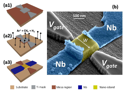
The nanofabrication of the hybrid S-QPC-S JJs required a series of three mutually aligned steps of electron beam lithography (EBL) sketched in Fig. 1 [(a1)-(a3)]. Fornieri Ni/AuGe/Ni/Au ohmics contacts were obtained in a single EBL operation followed by a subsequent aligned EBL step in order to define the semiconductor mesa into a QPC geometry with two lateral side-gates. A Ti mask was deposited by thermal evaporation [see Fig. 1 (a1)] and the heterostructure was then etched through reactive ion etching in Ar+/H2/CH4 atmosphere Carillo-PE ; Fornieri [see Fig. 1 (a2)]. The Ti mask was then removed by a : HF:H2O solution sample rinse. The resulting QPC mesa had a typical length of m, smaller than the elastic mean free path . The third and last aligned step of lithography [see Fig. 1 (a3)] was fulfilled to laterally contact the 2DEG with two Nb electrodes, that were deposited by sputtering (with a previous dip into a : HF:H2O solution and a low-energy Ar+ cleaning of the surface) with a growth rate of nm/s. A pseudo-color scanning electron micrograph of one typical device is shown in Fig. 1 (b). The superconducting gap of the Nb leads, of meV, yields a value of the superconducting coherence length nm (the Fermi velocity m/s). Low temperature magneto-electric characterization was performed in a filtered dilution refrigerator down to mK. 4-wire measurements were performed with the structure current-biased. The voltage drop across the junction was measured with a room-temperature differential preamplifier. Moreover, an external magnetic field was applied perpendicularly to the 2DEG plane to explore the Josephson current interference. The two side gates were used to deplete the 2DEG region of the QPC by biasing them negatively in voltage.
Table 1 shows the essential physical parameters of all four devices (A to D) studied in this work. The transmissivity () has been indirectly estimated both from the excess current and the Sharvin resistance and presents a consistent value in all the devices.
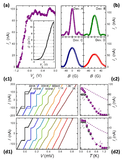
Figure 2 (a) displays the evolution of the Josephson critical current () as a function of the gate voltage () measured without external magnetic field. The Josephson coupling decreases noticeably by shrinking the QPC and disappears for V. The averaged conductance () in device A, extracted from different characteristics, is shown in the inset. was measured in the regime of Josephson coupling suppression, at G. Some conductance plateaus can be noted and the full suppression of is obtained when driving the QPC into the pinch-off regime at V. The other devices display similar characteristics. Figure 2 (b) shows the evolution of vs. for all the four devices. Devices A and B, which have a width nm, show a Fraunhofer-like pattern whereas the narrower junctions (device C and D having a nm) exhibit a monotonic decay interference pattern. Figure. 2 displays a selection of the current-voltage characteristics for devices A (c1) and D (d1) with the temperature spanning from mK to K. cooldown . The Josephson coupling survives up to K for both junctions whereas traces of superconductivity persists at greater . The temperature evolution for the switching () and re-trapping current () is shown in Fig. 2 (c1) (device A) and (d1) (device D). A noticeable hysteretic behavior is present in device A and B for temperatures below mK whereas in C and D for almost the whole range of . We observed that quasiparticle heating in the 2DEG region when the junction switches into the dissipative regime Courtois-PRL manifests mainly in the wider junctions. Dashed lines represent the theoretical temperature evolution of accordingly to the model of Chrestin et al. Chrestin-PRB calculated with the nominal values of meV, , and . The only fitting parameter is the value of the interface scattering parameter Flensberg-PRB ( for device A and for device D) yielding transparency of the interfaces of , thus, in very good agreement with the values extracted experimentally from (Table 1). At low temperature, the model recovers the experimental value for the maximum supercurrent in both junctions while the reduction predicted theoretically by increasing is much less pronounced than that observed experimentally.

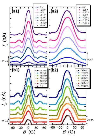
Figure 3 shows the evolution of the characteristics measured at mK for a few selected values of in devices A (a1) and C (a2). Device A exhibits the Fraunhofer-like interference pattern and by depleting the N-region (applying a negative voltage drop to the side gates) the pattern evolves to the one typically observed in narrow-junctions. Device C displays the Fraunhofer-like interference pattern for V with the second peak barely visible, and dramatically switches to a pattern characterized by a monotonic decay when shrinking the QPC further. From the position of the first zero in magnetic field of the pattern in Fig. 3 (a1) we can estimate the expected area of the proximized N-region from the expression , with Wb the superconducting flux quantum. At V turns out to be G thus m2 that matches perfectly with the physical dimensions of device A and B. By depleting the QPC the position of the first minimum evolves to higher values of . At V, the first minimum of the interference pattern manifests at G yielding a value for m2 which coincides with the area enclosed within N-region in the narrower junctions (device C and D). As we are depleting the N-region by electrostatic fields applied perpendicularly to the direction of the Josephson current, the evolution of the magnetic interference pattern is ascribed to the shrinkage of the effective width in the N-region.

To support our conclusions we now proceed to compare the experimental results with those obtained from a theoretical model introduced by Barzykin and Zagoskin Barzykin . This model predicts the evolution of the magnetic interference pattern as a function of the length-to-width ratio and temperature in ballistic mesoscopic SNS junctions. The expression for the Josephson current passing through the JJ is:
| (1) |
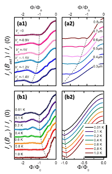
where with () the position at the left (right) S-N interface, , nm and . Figure 4 (a1) displays the experimental evolution of the characteristic normalized to the value at for a few selected values of . In Fig. 4(a2) we show the evolution of the curves for different values of calculated from Eq. 1. Gray dashed lines appear as a guide for the eye and show the evolution of the first interference pattern minimum. We note a good qualitative agreement between theory and experiment. The electrostatic shrinkage of the junction by the application of negative voltages in the side gates is equivalent to a physical reduction of the width of the junction, thus, a reduction of the number of conducting channels present in the system. By contrast, in Fig. 4 [(b1)-(b2)] we display the normalized characteristics [experimental (b1) and theoretical (b2)] for a few selected values of . Gray dashed lines appear again as a guide for the eye for the position of the first minimum of . The theoretical curves obtained from Eq. 1 captures qualitatively the experimental evolution also as a function of temperature with the first minimum of the interference pattern displacing towards when decreasing the temperature. The model, although rather idealized, is therefore an useful tool to grasp the physical picture at the basis of our junction’s behavior.
In summary, we have reported the magneto-electrostatic tailoring of the supercurrent in ballistic nanofabricated JJ QPCs based on an InAs heterostructure laterally contacted to superconducting Nb leads. The depletion of the N-region by biasing negatively the two etched side gates allows us, in combination with the application of a perpendicular , to tune the magnetic interference pattern continuously. We have demonstrated that for wider junctions the supercurrent displays a Fraunhofer-like interference pattern with periodicity whereas by shrinking the QPC, the interference pattern evolves continuously up to a monotonic-like decay typical of narrower junctions as theoretically predicted. Cuevas-PRL The evolution of as a function of and in such samples has been qualitatively explained by a simple theoretical model that captures the underlying physics. Barzykin
We thank R. Aguado, D. Esteve, M. Goffman, P. Joyez, H. Pothier and C. Urbina for fruitful discussions. Partial financial support from the FP7 program No. 228464 ”MICROKELVIN”, from the Italian Ministry of Defence through the PNRM project ”TERASUPER” and for the POR CRO FSE 2007-2013 project ”TERASQUID” is acknowledged.
References
- (1) Y. Oreg, J. D. Sau, and S. Das Sarma, Phys. Rev. Lett. 107, 177002 (2011).
- (2) M. Wimmer, A. R. Akhmerov, J. P. Dahlhaus, and C. W. J. Beenakker, New J. Phys. 13, 053016 (2011).
- (3) J. Alicea, Rep. Prog. Phys. 75, 076501 (2012).
- (4) C. W. J. Beenakker arXiv:1112.1950v2 [cond-mat.mes-hall].
- (5) V. Mourik, K. Zuo, S. M. Frolov, S. R. Plissard, E. P. A. M. Bakkers, and L. P. Kouwenhoven, Science 336, 1003 (2012).
- (6) L. P. Rokhinson, Xinyu Liu, and J. Furdyna, Nature Phys. 8, 795 (2012).
- (7) M. T. Deng, C. L. Yu, G. Y. Huang, M. Larsson, P. Caroff, and H. Q. Xu, Nano Lett. 12 6414 (2012).
- (8) A. Das, Y. Ronen, Y. Most, Y. Oreg, M. Heiblum, and H. Shtrikman, Nature Phys. 8, 887 (2012).
- (9) For a review see Th. Schäpers, Superconductor-semiconductor junctions (Springer, Berlin) (2001) and references therein.
- (10) H. Takayanagi, T. Akazaki, and J. Nitta, Phys. Rev. Lett. 75, 3533 (1995).
- (11) C. W. J. Beenakker and H. van Houten, Phys. Rev. Lett. 66, 3056 (1991).
- (12) T. Bauch, E. Hürfeld, V. M. Krasnov, P. Delsing, H. Takayanagi, and T. Akazaki, Phys. Rev. B 71, 174502 (2005).
- (13) J. P. Heida, B. J. van Wees, T. M. Klapwijk, and G. Borghs, Phys. Rev. B 57, 5618R (1998).
- (14) Y. Harada, S. Jensen, T. Akazaki, and H. Takayanagi, Physica C 367, 229 (2002).
- (15) F. Rohlfing, G. Tkachov, F. Otto, K. Richter, D. Weiss, G. Borghs, and C. Strunk, Phys. Rev. B 80, 220507(R) (2009).
- (16) J. C. Cuevas, and F. S. Bergeret, Phys. Rev. Lett. 99, 217002 (2007).
- (17) F. Deon, V. Pellegrini, F. Giazotto, G. Biasiol, L. Sorba, and F. Beltram, Phys. Rev. B. 84, 100506(R) (2011).
- (18) F. Capotondi, G. Biasiol, D. Ercolani, V. Grillo, E. Carlino, F. Romanato, and L. Sorba, Thin Solid Films 484, 400 (2005).
- (19) F. Capotondi, G. Biasiol, D. Ercolani, and L. Sorba, J. Cryst. Growth 278, 538 (2005).
- (20) A. Fornieri, M. Amado, F. Carillo, F. Dolcini, G. Biasiol, L. Sorba, V. Pellegrini, and F. Giazotto, arXiv:1211.1629.
- (21) F. Carillo, G. Biasiol, D. Frustaglia, F. Giazotto, L. Sorba, and F. Beltram, Physica E 32, 53 (2006).
- (22) K. Flensberg, J. Bindslev Hansen, and M. Octavio, Phys. Rev. B 38, 8707 (1988).
- (23) The measurements were performed in different cool downs thus the electronic configuration of the 2DEG did not remain unchanged all along the realization of this work. Therefore, the maximum critical current found for a single device could slightly vary at a given temperature within the different figures.
- (24) H. Courtois, M. Meschke, J. T. Peltonen, and J. P. Pekola, Phys. Rev. Lett. 101, 067002 (2008).
- (25) A. Chrestin, T. Matsuyama, and U. Merkt, Phys. Rev. B. 49, 498 (1994).
- (26) V. Barzykin and A. M. Zagoskin, Superlattices Microstruct. 25, 797 (1999).