Rashba split surface states in BiTeBr
Abstract
Within density functional theory, we study bulk band structure and surface states of BiTeBr. We consider both ordered and disordered phases which differ in atomic order in the Te-Br sublattice. On the basis of relativistic ab-initio calculations, we show that the ordered BiTeBr is energetically preferable as compared with the disordered one. We demonstrate that both Te- and Br-terminated surfaces of the ordered BiTeBr hold surface states with a giant spin-orbit splitting. The Te-terminated surface-state spin splitting has the Rashba-type behavior with the coupling parameter eVÅ.
pacs:
73.20.-r, 75.70.TjI Introduction
Nowadays, a controllable manipulation of the electronic spin degree-of-freedom without recourse to an external magnetic field is a process in technological demand, since it constitutes the basis of functionality of spintronics devices Zutic_2004 . An obvious candidate for the phenomenon underlying this process is spin-orbit interaction (SOI) that couples spin and momentum of electrons. In the case of two-dimensional (2D) geometries (surfaces, asymmetric quantum wells, etc.), the SOI may result in a spin splitting of electron states, which has a nature of the so-called Rashba effect Rashba_1960_1984 . This splitting can be tuned by an applied electric field Caviglia_PRL_2010 ; Studer_PRL2009 ; Grundler_PRL_2000 ; Datta_1990 ; Nitta_1997 , which opens a pathway for realizing electric-field spin manipulation. There are two key operating characteristics here: the Rashba energy, , and the momentum offset of split states, , which together define the Rashba coupling strength as .
In the conventional semiconductor structures, where the Rashba effect has been revealed for the first time, the parameter is of order of eVÅ (see, e.g., Refs. Lommer_PRL_1988 ; Luo_PRB_1990 ; Nitta_1997 ). However, for room-temperature applications of spintronics devices, it is crucial to have as large as possible. As a result, over a long period of time the Rashba effect keeps attracting a great interest, and many systems with a large Rashba spin splitting have been discovered. It was found that the surface state on Au(111) has a Rashba splitting with that is about five times larger than that in the semiconductor heterostructures (see, e.g., Refs. LaShell_PRL_1996 ; Nicolay_PRB_2001 ; Hoesch_PRB_2004 ). A larger (half as much as that for Au(111)) has been reported for a surface state at the Bi(111) surface Koroteev_PRL_2004 . In seeking a way to tune spin-orbit-splitting of surface states, it was shown that, for instance, in the case of the Au(111) surface it can be done with deposition of Ag-atoms Cercellier_PRB_2004 ; Popovich_PRB_2005 . As was demonstrated in Refs. Nakagawa_PRB_2007 ; Ast_PRL_2007 ; Bihlmayer_PRB_2007 ; Ast_PRB_2008 ; Mirhosseini_PRB_2009 ; Gierz_PRB_2010 ; Bentmann_PRB_2011 , a more effective way to modify spin splitting of surface states is a surface alloying of heavy elements (Bi, Pb, Sb) on noble-metal surfaces. In this case, one arrives at a Rashba-type split surface state with that is about one order of magnitude greater than that in the semiconductor structures.
To go further in possible tuning of spin-orbit-splitting of electron states, quantum-well states evolving by the confinement of electrons in ultrathin metal films have been considered. In the presence of both the surface and the interface with a substrate, a number of impacts on the splitting doubles. As was reported, e.g., in Ref. Mathias_PRL_2010 , a Bi monolayer film on Cu(111) can provide with spin-orbit-split quantum-well states in the unoccupied electronic structure, which are characterized by similar to that in the surface alloys. However, apart from a large spin-orbit splitting, for an efficient spintronics application in the way specified above a semiconductor substrate and the absence of spin-degenerate carriers in a quite wide energy interval are more promising.
In the case of semiconductor substrate (e.g., an ultrathin Pb films on Si(111) Dil_PRL_2008 ) quantum well states show a Rashba splitting as small as in the semiconductor structures. A large Rashba spin splitting on a semiconductor substrate can be reached, for example, by means of a Bi-trimer adlayer on a Si(111) surface (see also Ref. Yaji_NatComm_2010 ), where the splitting has a similar origin as in the Bi/Ag(111) surface alloy and a close value for the parameter Gierz_PRL_2009 . Nevertheless, the found spin-split 2D states cannot be well described by a simple Rashba model, where a parabolic dispersion with a positive effective mass combines with the spin-splitting that is linear in electron momentum. This motivates an active search of new materials and a revision of the already known systems with a SOI that under certain conditions can lead to a technologically meaningful spin spliting of a free-electron-like state at a semiconductor surface. In that sense, the reexamining of bismuth tellurohalides, where a Rashba-type spin splitting of states has been revealed to be caused by intrinsic inversion asymmetry of bulk crystal potential NatMat_BiTeI ; Bahramy , can be considered as a great advance made recently in the search. Actually, it was shown that Te-terminated surfaces of BiTeCl and BiTeI possess a giant spin-orbit splitting of a free-electron-like surface state Eremeev_PRL ; Crepaldi_PRL ; Landolt_PRL ; Eremeev_JETPlett .
The mentioned bismuth tellurohalides have hexagonal crystal structures Shevelkov and are characterized by ionic bonding with large charge transfer from Bi to halide- and Te-atomic layers. The crystal structure is built up of alternating hexagonal layers Te-Bi-I(Cl) stacked along the hexagonal axis. Besides, each three layers Te-Bi-I(Cl) form a three-layer (TL) block, and the distance between the blocks is about one and a half times greater than the interlayer distances within the Te-Bi-I(Cl) TL structure. Such a three-layered structure breaks the inversion symmetry of bulk crystal potential, which leads to appearing of the Rashba-type spin-orbit splitting of the bulk bands NatMat_BiTeI . Due to the layered crystal structure, the bismuth tellurohalide surfaces can be terminated by Te- or halide-atom-layer. Both these terminations hold spin-split surface states Eremeev_PRL ; Crepaldi_PRL ; Landolt_PRL ; Eremeev_JETPlett . These states emerge by splitting off either from the lowest conduction band (for the Te-termination) or from the uppermost valence band (for the halide-atom-termination). The splitting off is caused by changes in potential (decreasing at the Te-terminated surface and increasing at the halide-atom-terminated surface) within the near-surface layers Eremeev_PRL as compared with the bulk region, which is a consequence of strong ionicity.
In addition to BiTeCl and BiTeI, the bismuth-tellurohalide group is known to have one more semiconductor—BiTeBr. It was previously reported Shevelkov ; Donges that its layered crystal structure is a disordered centrosymmetric one, where tellurium and bromine atoms randomly distributed within two layers adjacent to Bi-atomic layer Shevelkov ; Donges . As a consequence, both the bulk and surface electronic structure of the disordered BiTeBr was never addressed before. Recently, bulk electronic structure of the ordered BiTeBr has been calculated and Rashba-type splitting of some bands has been analyzed Eremeev_PRL .
In the present paper, we examine both disordered and ordered phases of BiTeBr. We model the crystal structure of the ordered phase as that of BiTeI but with Br instead of I and the lattice parameters were taken form Ref. Shevelkov , at that atomic positions are obtained within a structural optimization. On the basis of ab-initio calculations we show that the ordered structure is energetically preferable. We demonstrate that both the Te- and Br-terminated surfaces of the ordered BiTeBr hold the spin-orbit split surface states emerged by splitting off from the bulk conduction or valence band like in other bismuth tellurohalides. For the practical use, as in the case of BiTeCl and BiTeI the Te-terminated surface of BiTeBr is more suitable than the halide-atom-terminated one, since it holds a surface state that has a free-electron-like dispersion and a large Rashba-type spin splitting. At the same time, BiTeBr has an advantage over BiTeCl and BiTeI. As compared with BiTeCl, the bromide has a larger Rashba spin splitting of the Te-terminated surface state and a wider bulk band gap. In contrast to BiTeI, the surface state is larger split off from the bulk conduction band and more isotropic.
II Computational method
The structural optimization and electronic band calculations are performed within the density functional formalism as implemented in VASP VASP1 ; VASP2 . We use the all-electron projector augmented wave (PAW) PAW1 ; PAW2 basis sets with the generalized gradient approximation (GGA) of Perdew, Burke, and Ernzerhof (PBE) GGA_PBE to the exchange correlation (XC) potential. The Hamiltonian contains the scalar relativistic corrections, and the SOI was taken into account by the second variation method KH .
To treat the bulk disordered phase effect, we employ two approaches. The first one is a supercell approach used within VASP, where supercell with several configurations for randomly distributed Te and Br atoms were considered. The second approach is a virtual crystal approximation (VCA) as implemented in the ABINIT code abinit1 , where the configuration averaged potential of a gray atom occupying a site in the Te-Br sublattice is defined as a mixture of Br () and Te () pseudopotentials with . We used GGA-PBE Hartwigsen-Goedecker-Hutter (HGH) HGH relativistic norm-conserving pseudopotentials taken from Ref. PSP_HGH which include the SOI.
The surface of the ordered BiTeBr formed under cleavage can have Te-layer or Br-layer termination. To simulate semi-infinite BiTeBr(0001), using VASP we consider a 24 atomic layer slab with bromine side (for Te-terminated surface) or tellurium side (for Br-terminated surface) passivated by hydrogen monolayer.
III Calculation results and discussion
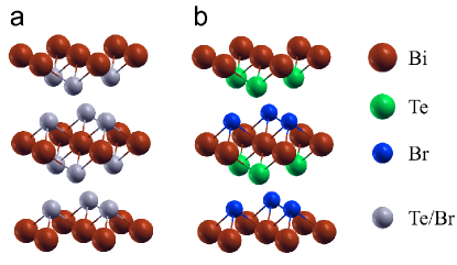
In earlier works Shevelkov ; Donges , the CdI2 hexagonal structure for BiTeBr was reported. This structure differs from that of BiTeI in that Br and Te atoms are statistically distributed over I2-type sites (Fig. 1(a)). According to Ref. Shevelkov , the mixed Te/Br layers are located at a distance of 1.806 Å from central Bi layer. To study the geometry of the disordered phase, we constructed a set of supercells with different configurations of randomly distributed Te and Br atoms. The simulation shows that owing to markedly different charge transfer from Bi atom to Br and Te atoms, the Bi layer acquires a substantial rippling of Å. This value is larger than the rippling within the Te/Br layer, which amounts to Å. Such a huge corrugation of atomic layers leads to a remarkable variation (from 1.3 to 2 Å) of the distance between Bi atoms of the central rippled layer and atoms of adjacent Te/Br layer. As a consequence, the resulting atomic structure differs essentially from that predicted in Ref. Shevelkov . Next we considered the BiTeI-type ordered structure (Fig. 1(b)). In this system, interlayer distances obtained within the structural optimization are 1.769 Å between Bi and Te layers and 1.917 Å between Bi and Br layers. The ordered BiTeBr gains an energy of meV per formula unit with respect to the disordered supercells. The VCA calculation confirms the preference of the ordered phase.
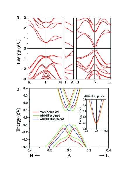
In Fig. 2(a), we show the bulk band structure calculated by VASP code for the ordered BiTeBr. As clearly seen in the figure, both the conduction band minimum (CBM) and the valence band maximum (VBM) demonstrate a giant Rashba-type spin splitting in the H-A-L plane. This spin splitting is characterized by a slightly anisotropic momentum offset that in A-H and A-L directions is of and Å-1 for the VBM and the CBM, respectively. The Rashba energy for the VBM is approximately twice of that for the CBM (111 meV vs 66 meV). As a result, it provides noticeably larger spin-orbit coupling for the upper valence-band states as compared with the lower conduction-band states (see Tabl. 1).
As seen in the Fig. 2(b), the pseudopotential ABINIT calculations performed for the ordered BiTeBr confirm the large spin-orbit splitting in the vicinity of the A point. Moreover, we have obtained values for the Rashba parameters, which are very close to those found with VASP (see in Tabl. 1). The bulk band gap evaluated by ABINIT is about 100 meV smaller than that obtained from the VASP calculations. The spectrum calculated within the VCA for the disordered phase shows practically the same band gap and demonstrates the expected lack of spin-splitting of the bulk bands due to the presence of inversion symmetry in the disordered structure. Note that the spin-splitting of the bulk bands obtained within supercell approach is negligible, and it agrees well with the VCA result (Fig. 2(b), inset), which indicates that chosen geometry is well suited for describing the disordered BiTeBr.
| (meV) | valence band | conduction band | |||
|---|---|---|---|---|---|
| A-H | A-L | A-H | A-L | ||
| VASP | 283 | 4.33 | 4.36 | 3.52 | 3.57 |
| ABINIT | 187 | 4.72 | 4.93 | 3.97 | 4.06 |
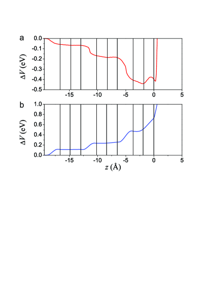
As was mentioned above, the spin-split surface states of BiTeI and BiTeCl emerge as a result of splitting off from the lowest conduction band (at the Te-terminated surface) or from the uppermost valence band (at the halide-atom-terminated surface). The splitting off is caused by the potential change, , in the near-surface layers of the crystal with respect to that in central, bulk-like layers. Such a potential change is negative at the Te-terminated surface and positive at the Cl(I) atom-terminated surface Eremeev_PRL ; Eremeev_JETPlett , at that bears a stepwise character owing to clearly defined three-layered structure of bismuth tellurohalides. A similar behavior of occurs on the surfaces of the ordered BiTeBr, as seen in Fig. 3, where the change of the potential within the three outermost TLs on both surface terminations is shown.
The negative observed at the Te-terminated surface of the ordered BiTeBr leads to a downward shift of energies of the electron states trapped in the stepwise surface potential (Fig. 4(a)). These states are predominantly localized in the first three TLs. At the Br-terminated surface, an upward shift of energies of the trapped states is provided by the positive (Fig. 4(b)). The trapped states are offset in momentum, reflecting a large bulk spin-orbit splitting. They appear partially overlapping the valence band continuum except the local energy gap regions within bulk continuum states where the trapped states can be well resolved in ARPES at high binding energies. As a net result, for both terminations the changes of the electronic structure of BiTeBr under the surface formation lead to emergence of the spin-split surface states in the bulk band gap (Fig. 5).

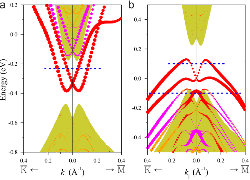
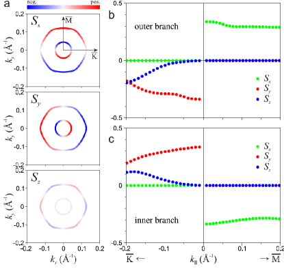
At the Te-terminated surface (Fig. 5(a)), the spin-orbit split surface state localized in the topmost TL replicates the conduction band edge. The degeneracy point of the surface spin-split state is 150 meV lower than the CBM. Within the energy gap region, the surface-state dispersion demonstrates the free-electron-like parabolic character. The spin splitting of the state is characterized by and 2.007 eVÅ in the and directions, respectively.
The parabolic character of the surface state provides circular shape of the constant energy contours (CEC) for inner and outer branches of the spin-split surface state in the bulk band gap region. As one can see in Fig. 6(a), in approaching the bulk conduction band the CEC for the outer branch acquires the hexagonal deformation that is already visible at 100 meV above the degeneracy point. The surface-state spin structure demonstrates counter-clockwise and clockwise in-plane helicity for the inner and outer branches, respectively, with a small spin component for both of them (Fig. 6(a)). Owing to symmetry constrains, the expectation value of the and spin components vanishes along , and they have maximal values along at any chosen energy. In turn, is zero along and reaches maximal values along direction. In Fig. 6(b), we show the absolute value of the cartesian spin components as functions of for the inner and outer branches of the spin-split surface state. As one can see, for a small the component is negligibly small, and, thus, the surface state is completely in-plane spin polarized. This component starts rising at Å-1, i.e. at energy of 50 meV above the degeneracy point, which leads to a decrease of the in-plane spin components under approaching the bulk conduction states. Thus, owing to (i) the parabolic energy dispersion, (ii) outermost TL localization, and (iii) the in-plane helical spin structure within the band gap energy region, the surface state on the Te-terminated surface of BiTeBr(0001) can be described as the Rashba-split surface state with Rashba coupling parameter of eVÅ.
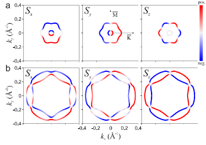
At the Br-terminated surface (Fig. 5(b)), the spin-orbit split surface state localized in the topmost TL lies entirely in the band gap right above the upper valence band and follows its edge. As one can see, the states localized in the second TL spread already along the valence-band edge in and directions but they degenerate with bulk states in the close vicinity of . Furthermore, the second outermost-TL localized state arises at in the valley of the valence band. The appearance of the second pair of the spin-split states in the gap and the second state at is explained by the fact that the magnitude of the is larger than that on the Te-terminated surface (see Fig. 3). Such a provides a larger splitting off from the valence band edge.
In general features, the band-gap-lying outermost TL-localized spin-orbit split surface state at the Br-terminated surface resembles those found at the halide-atom-terminated surface of BiTeCl and BiTeI Eremeev_PRL ; Eremeev_JETPlett . This state demonstrates noticeable anisotropy of the energy dispersion with respect to , which results in more complex shape of the CECs both above and below the degeneracy point (see Fig. 7). Such an anisotropic dispersion is accompanied by an appreciably out-of-plane spin polarization and entangled spin structure of the surface state, especially below the degeneracy point (Fig. 7).
Formally, the spin-splitting of the Br-terminated surface state is characterized by = 0.079 and 0.077 Å-1 in and direction, respectively, and by equal to 130.2 meV () and 125.6 meV (). These characteristics yield equal to 3.29 and 3.26 eVÅ for and directions, respectively. However, this spin-split surface state can not be identified as the Rashba state owing to its dispersion and entangled spin structure.
IV Conclusions
Thus, we have investigated the atomic and electronic structure of BiTeBr. The total energy calculations of the ordered and disordered phases of BiTeBr have shown that the ordered structure is energetically preferable. We have found that the surfaces of the ordered BiTeBr hold surface states which demonstrate a giant spin-orbit spin splitting. These states emerge as a result of splitting off from the bulk conduction or valence band, owing to the potential bending within the near-surface layers, like in other bismuth tellurohalides, BiTeCl and BiTeI, studied earlier. The spin-split surface state at the Te-terminated surface, owing to its parabolic energy dispersion, outermost TL localization, and in-plane helical spin structure preserved within the whole band-gap energy region, can be described as a Rashba-split surface state with the Rashba coupling parameter of eVÅ which is in a good agreement with recently reported experimental value of 2.0(7) eVÅSakano_arxiv . The Rashba-split state on Te-terminated BiTeBr has advantages over the other bismuth tellurohalides, which consist in the larger Rashba splitting and wider band gap as compared to BiTeCl and in the larger splitting off from the bulk conduction band with more isotropic energy dispersion within the band gap region in comparison with BiTeI.
The band gap surface state at the Br-terminated surface owing to its anisotropy and entangled spin structure can not be identified as the Rashba-split state and thus has less appeal than the spin split surface state at the Te-terminated surface.
References
- (1) I. Žutić, J. Fabian, and S. Das Sarma, Rev. Mod.. Phys. 76, 323 (2004).
- (2) E.I. Rashba, Sov. Phys. Solid State 2, 1109 (1960); Y.A. Bychkov and E.I. Rashba, JETP Lett. 39, 78 (1984); J. Phys. C 17, 6039 (1984).
- (3) S. Datta and B. Das, Appl. Phys. Lett. 56, 665 (1990).
- (4) J. Nitta, T. Akazaki, H. Takayanagi, and T. Enoki, Phys. Rev. Lett. 78, 1335 (1997).
- (5) D. Grundler, Phys. Rev. Lett. 84, 6074 (2000).
- (6) M. Studer, G. Salis, K. Ensslin, D.C. Driscoll, and A.C. Gossard, Phys. Rev. Lett. 103, 027201 (2009).
- (7) A. D. Caviglia, M. Gabay, S. Gariglio, N. Reyren, C. Cancellieri, and J.-M. Triscone, Phys. Rev. Lett. 104, 126803 (2010).
- (8) G. Lommer, F. Malcher, and U. Rossler, Phys. Rev. Lett. 60, 728 (1988).
- (9) J. Luo, H. Munekata, F.F. Fang, and P.J. Stiles, Phys. Rev. B 41, 7685 (1990).
- (10) S. LaShell, B.A. McDougall, and E. Jensen, Phys. Rev. Lett. 77, 3419 (1996).
- (11) G. Nicolay, F. Reinert, and S. Hüfner, P. Blaha, Phys. Rev. B 65, 033407 (2001).
- (12) M. Hoesch, M. Muntwiler, V.N. Petrov, M. Hengsberger, L. Patthey, M. Shi, M. Falub, T. Greber, and J. Osterwalder, Phys. Rev. B 69, 241401(R) (2004).
- (13) Yu.M. Koroteev, G. Bihlmayer, J.E. Gayone, E.V. Chulkov, S. Blügel, P.M. Echenique, and Ph. Hofmann, Phys. Rev. Lett. 93, 046403 (2004).
- (14) H. Cercellier, Y. Fagot-Revurat, B. Kierren, F. Reinert, D. Popović, and D. Malterre, Phys. Rev. B 70, 193412 (2004).
- (15) D. Popović, F. Reinert, S. Hüfner, V. G. Grigoryan, M. Springborg, H. Cercellier, Y. Fagot-Revurat, B. Kierren, and D. Malterre, Phys. Rev. B 72, 045419 (2005).
- (16) T. Nakagawa, O. Ohgami, Y. Saito, H. Okuyama, M. Nishijima, and T. Aruga, Phys. Rev. B 75, 155409 (2007).
- (17) C. R. Ast, J. Henk, A. Ernst, L. Moreschini, M. C. Falub, D. Pacilé, P. Bruno, K. Kern, M. Grioni, Phys. Rev. Lett. 98, 186807 (2007).
- (18) G. Bihlmayer, S. Blügel, and E. V. Chulkov, Phys. Rev. B 75, 195414 (2007).
- (19) C. R. Ast, D. Pacilé, L. Moreschini, M. C. Falub, M. Papagno, K. Kern, M. Grioni, J. Henk, A. Ernst, S. Ostanin, and P. Bruno, Phys. Rev. B 77, 081407(R) (2008).
- (20) H. Mirhosseini, J. Henk, A. Ernst, S. Ostanin, C.-T. Chiang, P. Yu, A. Winkelmann, and J. Kirschner, Phys. Rev. B 79, 245428 (2009).
- (21) H. Bentmann, T. Kuzumaki, G. Bihlmayer, S. Blügel, E. V. Chulkov, F. Reinert, and K. Sakamoto, Phys. Rev. B 84, 115426 (2011).
- (22) I. Gierz, B. Stadtmüller, J. Vuorinen, M. Lindroos, F. Meier, J. H. Dil, K. Kern, and C. R. Ast, Phys. Rev. B 81, 245430 (2010).
- (23) S. Mathias, A. Ruffing, F. Deicke, M. Wiesenmayer, I. Sakar, G. Bihlmayer, E.V. Chulkov, Yu.M. Koroteev, P. M. Echenique, M. Bauer, and M. Aeschlimann, Phys. Rev. Lett. 104, 066802 (2010).
- (24) J. H. Dil, F. Meier, J. Lobo-Checa, L. Patthey, G. Bihlmayer, and J. Osterwalder, Phys. Rev. Lett. 101, 266802 (2008).
- (25) K. Yaji, Y. Ohtsubo, Sh. Hatta, H. Okuyama, K. Miyamoto, T. Okuda, A. Kimura, H. Namatame, M. Taniguchi, and T. Aruga, Nat. Commun. 1:17 doi: 10.1038/ncomms1016 (2010).
- (26) I. Gierz, T. Suzuki, E. Frantzeskakis, S. Pons, S. Ostanin, A. Ernst, J. Henk, M. Grioni, K. Kern, and C. R. Ast, Phys. Rev. Lett. 103, 046803 (2009).
- (27) K. Ishizaka, M.S. Bahramy, H. Murakawa, M. Sakano, T. Shimojima, T. Sonobe, K. Koizumi, S. Shin, H. Miyahara, A. Kimura, K. Miyamoto, T. Okuda, H. Namatame, M. Taniguchi, R. Arita, N. Nagaosa, K. Kobayashi, Y. Murakami, R. Kumai, Y. Kaneko, Y. Onose and Y. Tokura, Nature Materials 10, 521 (2011).
- (28) M.S. Bahramy, R. Arita, and N. Nagaosa, Phys. Rev B 84, 041202(R) (2011).
- (29) S. V. Eremeev, I. A. Nechaev, Yu. M. Koroteev, P. M. Echenique, and E. V. Chulkov, Phys. Rev. Lett. 108, 246802 (2012).
- (30) A. Crepaldi, L. Moreschini, G. Auteè, C. Tournier-Colletta, S. Moser, N. Virk, H. Berger, Ph. Bugnon, Y. J. Chang, K. Kern, A. Bostwick, E. Rotenberg, O. V. Yazyev, and M. Grioni, Phys. Rev. Lett. 109, 096803 (2012).
- (31) G. Landolt, S. V. Eremeev, Y. M. Koroteev, B. Slomski, S. Muff, T. Neupert, M. Kobayashi, V. N. Strocov, T. Schmitt, Z. S. Aliev, M. B. Babanly, I. R. Amiraslanov, E. V. Chulkov, J. Osterwalder, and J. H. Dil, Phys. Rev. Lett. 109, 116403 (2012).
- (32) S. V. Eremeev, A. I. Nechaev, E. V. Chulkov, JETP Lett. 96, 437 (2012).
- (33) A.V. Shevelkov, E.V. Dikarev, R.V. Shpanchenko, and B.A. Popovkin, J. Solid State Chem. 114, 379 (1995).
- (34) E. Donges, Z. Anorg. Allg. Chem. 265, 56 (1951).
- (35) G. Kresse, J. Hafner, Phys. Rev. B 48, 13115 (1993).
- (36) G. Kresse, J. Furthmüller, Comput. Mater. Sci. 6, 15 (1996).
- (37) P.E. Blöchl, Phys. Rev. B 50, 17953 (1994).
- (38) G. Kresse, D. Joubert, Phys. Rev. B 59, 1758 (1999).
- (39) J.P. Perdew, K. Burke, and M. Ernzerhof, Phys. Rev. Lett. 77, 3865 (1996).
- (40) D.D. Koelling, B.N. Harmon, J. Phys. C: Solid State Phys. 10, 3107 (1977).
- (41) X. Gonze, B. Amadon, P.-M. Anglade, J.-M. Beuken, F. Bottin, P. Boulanger, F. Bruneval, D. Caliste, R. Caracas, M. Cote, T. Deutsch, L. Genovese, Ph. Ghosez, M. Giantomassi, S. Goedecker, D.R. Hamann, P. Hermet, F. Jollet, G. Jomard, S. Leroux, M. Mancini, S. Mazevet, M.J.T. Oliveira, G. Onida, Y. Pouillon, T. Rangel, G.-M. Rignanese, D. Sangalli, R. Shaltaf, M. Torrent, M.J. Verstraete, G. Zerah, J.W. Zwanziger., Computer Phys. Commun. 180, 2582 (2009); http://www.abinit.org.
- (42) C. Hartwigsen, S. Goedecker and J. Hutter. Phys. Rev. B 58, 3641 (1998).
- (43) http://cvs.berlios.de/cgi-bin/viewvc.cgi/cp2k/potentials/ Goedecker/abinit/pbe/
- (44) M. Sakano, M. S. Bahramy, A. Katayama, T. Shimojima, H. Murakawa, Y. Kaneko, W. Malaeb, S. Shin, K. Ono, H. Kumigashira, R. Arita, N. Nagaosa, H. Y. Hwang, Y. Tokura, and K. Ishizaka, arXiv:1212.1552v1