Mode space approach for tight-binding transport simulations in graphene nanoribbon field-effect transistors including phonon scattering
Abstract
In this paper, we present a mode space method for atomistic non-equilibrium Green’s function simulations of armchair graphene nanoribbon FETs that includes electron-phonon scattering. With reference to both conventional and tunnel FET structures, we show that, in the ideal case of a smooth electrostatic potential, the modes can be decoupled in different groups without any loss of accuracy. Thus, inter-subband scattering due to electron-phonon interactions is properly accounted for, while the overall simulation time considerably improves with respect to real-space, with a speed-up factor of 40 for a -nm-wide device. Such factor increases with the square of the device width. We also discuss the accuracy of two commonly used approximations of the scattering self-energies: the neglect of the off-diagonal entries in the mode-space expressions and the neglect of the Hermitian part of the retarded self-energy. While the latter is an acceptable approximation in most bias conditions, the former is somewhat inaccurate when the device is in the off-state and optical phonon scattering is essential in determining the current via band-to-band tunneling. Finally, we show that, in the presence of a disordered potential, a coupled mode space approach is necessary, but the results are still accurate compared to the real-space solution.
I Introduction
Graphene nanoribbons (GNRs) have been proposed in recent years as a possible replacement for silicon in the future generation of field effect transistors Han et al. (2007); Chen et al. (2007). Despite the outstanding challenges in producing GNRs with controlled width and edges and the resulting degradation of the graphene intrinsic mobility, devices with large on-off current ratio have been successfully demonstrated Wang et al. (2008).
Theoretical performance of GNRFETs have been widely investigated by numerous simulation studies (e.g Refs. Fiori and Iannaccone, 2007; Ouyang et al., 2007; Liang et al., 2007; Yoon et al., 2008; Zhao et al., 2009; Grassi et al., 2009). The state-of-the-art approach for modeling the electronic properties of GNRs is based on an atomistic tight-binding (TB) Hamiltonian with a orbital basis set. The transport problem is usually solved within the nonequilibrium Green’s function formalism (NEGF) Datta (2005), which provides a rigorous framework for including incoherent scattering processes in the quantum description. TB simulations of GNRFETs including phonon scattering have been reported too Ouyang et al. (2008); Yoon et al. (2011); Yoon and Salahuddin (2012); Akhavan et al. (2012). Those simulations were performed using a real space (RS) approach. On the other hand, more efficient mode space (MS) methods would be preferable for use in intensive device simulations.
The MS approach is well established with reference to an effective mass (EM) Hamiltonian Wang et al. (2004); Luisier et al. (2006). It is based on the expansion of the Green’s functions in terms of the transverse eigenfunctions (modes) and it is most efficient when quantum confinement is relatively strong in the transverse plane, so that only few of the lowest subbands are occupied. The so-called coupled mode space (CMS) is the general method, while a more efficient version, the uncoupled mode space (UMS), can be adopted when the transverse potential profile is slightly varying along the transport direction. The inclusion of electron-phonon scattering in the MS EM model is also well known Jin et al. (2006); Poli (2009); Esposito et al. (2009); Nikonov et al. (2009); Afzalian (2011).
On the other hand, the MS approach is not generally applicable to a TB Hamiltonian. Due to the non-separable Hamiltonian, even when the potential is uniform along the longitudinal direction (so that the longitudinal wavevector is conserved), the wavefunctions at different in the same subband are in general different. In other words, by defining the modes as the transverse part of the wavefunctions at a particular , the wavefunctions at the generic are a linear combination of them. This is similar to what occurs in the case of a Hamiltonian Shin (2009). Nevertheless, for the particular case of the TB Hamiltonian of GNRs with armchair edges, we have previously shown by numerical calculation that a MS method is actually possible, since each subband contains only few modes Grassi et al. (2011). A formal derivation was given in Ref. Zhao and Guo, 2009 using analytically defined modes.
In this paper, we propose a novel MS method for the inclusion of graphene acoustic phonon (AP) and optical phonon (OP) scattering within the NEGF formalism, and test its accuracy with respect to RS in both the cases of smooth and disordered potentials. Two approximations commonly found in the literature for treating the scattering self-energy are also evaluated. The paper is organized as follows. Sec. II reviews the standard RS TB method as well as the MS TB method from Ref. Grassi et al., 2011, modified so as to include phonon scattering. Simulation results of GNRFETs are presented in Sec. III and conclusions are finally drawn in Sec. IV.
II Mathematical model
II.1 Real space formulation
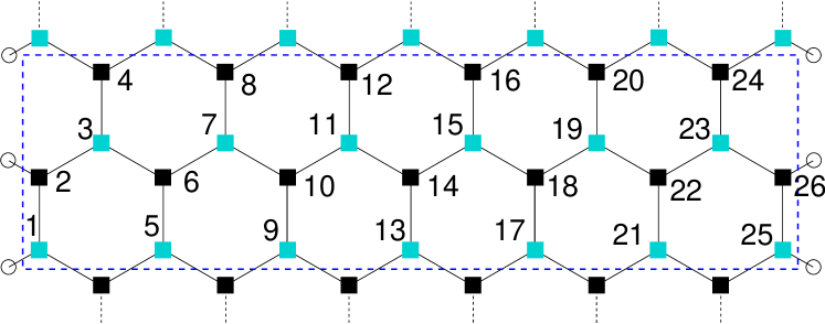
The atomic structure of an armchair GNR unit cell is shown for reference in Fig. 1. The GNR width is denoted by the number of dimer lines . We adopt the TB Hamiltonian model proposed in Ref. Son et al., 2006, which is based on a set of orthogonal orbitals, one for each atom, with hopping integrals limited to first nearest-neighbor orbitals and of value for internal atom pairs, and for atom pairs located along the edges of the GNR ( eV and ). The onsite energies are set equal to the value of the electrostatic potential energy at each atomic site. Unless stated otherwise, the electrostatic potential is calculated by self-consistently solving the 3D Poisson equation.
In order to calculate electron and hole densities within the NEGF formalism, the following equations need to be solved for the retarded, the lesser and the greater Green’s function matrices , and , respectively, for each energy
| (1) |
| (2) |
| (3) |
where denotes the restriction of the Hamiltonian matrix to the GNR portion inside the simulation domain and . Besides, and similarly for and , where are the self-energies for the semi-infinite source and drain leads, which are assumed in thermodynamic equilibrium, while account for phonon scattering. Calculation of both (2) and (3) is actually not needed, since either one of the two equations can be replaced by the identity .
Phonon scattering is treated within the self-consistent Born approximation. The model accounts for both OP and AP scattering, the latter within the elastic and high temperature limit, resulting in the following expressions of the lesser and greater phonon self energies
| (4) | |||||
| (5) | |||||
where indicates element-by-element matrix multiplication, is the OP occupation number, and and are given by
| (6) |
with eV the AP deformation potential, cm/s the sound velocity in graphene, the temperature, the carbon atomic mass, eV/cm and meV the zone-boundary OP deformation potential and energy, respectively. The retarded phonon self-energy is computed using the identity
| (7) |
where the symbol P stands for the principal part of the integral. Unless stated otherwise, we include the contribution to the principal part integral (Hermitian part of ) due to AP scattering, while we neglect the one due to OP scattering. See Appendix A for details on the numerical implementation of the principal part integral.
The equations above, namely (1)-(3) together with (4), (5) and (7), are iteratively solved. It is worth noticing that and can be ordered in a block tridiagonal and block diagonal form, respectively, each diagonal block having the size of the number of atoms in a specific transverse layer, or slab, of the GNR. Hence, the Recursive Green Function algorithm (RGF) Lake et al. (1997); Svizhenko et al. (2002) can be used to solve (1)-(3). In this paper, we consider each slab to be made of four rows of atoms, i.e. equal to the GNR unit cell (Fig. 1).
II.2 Mode space formulation
In this section the MS approach presented in Ref. Grassi et al., 2011, and in that paper discussed with reference to coherent transport simulations of GNRs, is extended to include phonon scattering.
The MS formulation starts by defining a set of orthonormal vectors, or modes, for each slab of the device. We choose the modes of the generic slab as the eigenvectors computed at of a fictitious GNR obtained by the periodic repetition (potential energy included) of that slab along the longitudinal direction. In the absence of topological differences between the slabs (such as edge irregularities or internal vacancies), the modes are the solution of the eigenvalue problem
| (8) |
where is the Hamiltonian block between slab and . Denoting by the matrix whose columns are the modes of layer , i.e. , a block-diagonal transformation matrix satisfying is constructed
| (9) |
with equal to the number of slabs.
In the following, we indicate with a tilde the MS matrices to distinguish them from the RS matrices. The CMS method consists in approximating (and similarly for and ) as
| (10) |
where is the solution of
| (11) |
with
| (12) | |||||
| (13) |
Eq. (11) is the MS version of (1). Analogous considerations apply to the other equations. Eq. (10) would be exact if was a square matrix. In practice, a mode truncation is performed so that and have a smaller size than their corresponding RS matrices and the solution of (11) instead of (1) is computationally advantageous. The computational time of the RGF algorithm scales as , where is the matrix block size Svizhenko et al. (2002), which is equal to the slab size for RS ( according to our choice of the slab size) and to the number of selected modes per slab for CMS. Thus, the speed-up of CMS compared to RS is a factor of the order of .
An algorithm to select the modes to retain in the matrix was presented in Ref. Grassi et al., 2011. It is based on identifying, among the modes calculated with zero electrostatic potential, the minimum set of modes that allow to reproduce with sufficient accuracy the subbands that lie in the energy range of interest. The mode indexes so identified are then used to select the actual modes calculated with the non-null electrostatic potential.
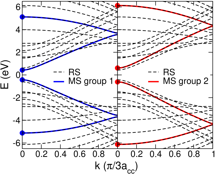
As shown in Fig. 2 for a GNR, it turns out that each one of the lowest conduction subbands at zero potential can be well reproduced by just four modes, which correspond to the eigenvalues at belonging to (i) the considered subband, (ii) the valence subband symmetrical to it, and (iii-iv) their respective folded continuations. Symmetrical considerations apply to the highest valence subbands. GNRs with different behave similarly. Since the sets of four modes described above, hereafter referred to as groups of modes, are disjoint from each other, a more efficient MS method, here called uncoupled group mode space (UGMS), can be obtained from (10)-(13) by neglecting the coupling between modes belonging to different groups. Let be the matrix whose columns are the modes in layer of group only. A transformation matrix similar to (9) is constructed by using the matrices as diagonal blocks. The UGMS method is derived by further approximating (10) as
| (14) |
where is the number of the considered groups and is the solution of
| (15) |
with
| (16) | |||||
| (17) |
In the UGMS method, the computational cost of the RGF algorithm scales as , where is the number of modes in each group. Hence, if the same number of modes is used, the speed-up of UGMS compared to CMS scales as , which can be sizeable for wide ribbons, since is proportional to the number of subbands that contribute to transport, which, in turn, is proportional to the GNR width.
In the following, we refer to the UGMS formulation, since the CMS one can be recovered from Eqs. (14)-(17) by considering all the selected modes as belonging to the same group and by setting . Note that and can be directly computed in MS without making use of (17). Instead, the calculation of is more complicated. In particular, in the MS representation these matrices are no longer diagonal, but just block diagonal. For example, as far as is concerned, from the equation for analogous to (17), using (4) and considering for simplicity the contribution of APs only (first term at the right-hand-side), with replaced by the equation analogous to (14), the following MS expression for the element relative to modes and of the diagonal matrix block associated with slab and group is derived
| (18) |
where the symbols and have been dropped for brevity and the form factor is defined by
| (19) |
( and are mode indexes within group , the atom index within the slab). Identical considerations apply to the OP terms and to the other types of phonon self-energies. It should be noticed that all the considered modes give their contribution to , not only those belonging to the same group of modes . This means that intersubband scattering between all considered modes is taken into account, without the necessity of going to full RS simulations. It must also be noticed that in the solution process the different mode groups can be treated independently, which is a great advantage compared to RS and also to CMS: at every iteration pass, once the Green functions for all groups have been calculated, the self-energies are updated using the equations like (18) collecting the contributions from all modes.
In the next section the MS and RS solutions will be compared in the presence of phonon scattering. A further approximation will be tested, which consists in simplifying the form factor as
| (20) |
where is the Kronecker delta, so that only the diagonal entries are kept in (18) and similar equations. This approximation is usually adopted in the context of the CMS EM approach due to its higher efficiency Jin et al. (2006); Poli (2009); Nikonov et al. (2009). The results obtained with expressions (19) and (20) will be named “MS2” and “MS1”, respectively.
III Results
All simulated devices have a double-gate structure with SiO2 1-nm-thick top and bottom oxides. As mentioned before, the source and drain are assumed to be semi-infinite leads. The portions of the source and drain regions included in the simulation domain are 10 nm long and uniformly doped. The channel is assumed to be intrinsic. Unless noted otherwise, the following device parameters are used: (corresponding to a ribbon width nm), gate length nm, and doping concentration in the source and drain regions equal to dopants per carbon atom. Also, unless stated otherwise, the MS method simulations are performed using the uncoupled group approximation (UGMS). For the reference GNR, the 2 groups of 4 modes of Fig. 2 are used (8 modes out of a total of 26 that correspond to the full RS solution). Both conventional FET and tunnel FET (TFET) devices are simulated. The latter have received great attention in recent years for their potential in low-power applications Zhao et al. (2009). The two structures only differ in the type of doping of the source region. While the drain is always n-type, the source is n-type and p-type for conventional FETs and TFETs, respectively.
We consider only ideal GNRs with perfect edges and no internal vacancies. Nevertheless, in the following, we also study the effect of adding a disorder potential to the TB Hamiltonian of the ideal GNR. Such disorder potential can, in principle, mimic the perturbation effect of impurities or the substrate.
III.1 Smooth electrostatic potential
The case of no disorder potential is treated first.
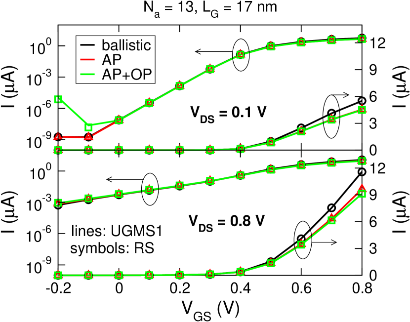
The vs. (“turn-on”) characteristics of a conventional n-i-n FET at and 0.8 V are plotted in Fig. 3. They are computed with the RS and the MS methods. For each method, we consider three transport conditions: (i) without scattering (i.e. ballistic transport), (ii) in the presence of only AP scattering, and (iii) in the presence of both AP and OP scattering. In the case of phonon scattering and MS approach, the simplified expression of the form-factor in (20) is used (MS1).
As regards the effect of phonon scattering and with reference to the RS results, it can be seen that AP scattering has only a limited effect on the current at this channel length, resulting in a ballisticity ratio (i.e. ratio between current in the presence of phonon scattering and ballistic current) of at V for both values. When also OP scattering is included, the current at high , i.e. on-state current, is only slightly decreased for the largest value. Similar findings were reported in Ref. Yoon et al., 2011. On the other hand, OP scattering is responsible for an increase of the minimum off-state current by a few orders of magnitudes when is low. This effect is caused by energy relaxation through emission or absorption of optical phonons, which favors band-to-band tunneling (BTBT) and shifts toward positive values the onset of the ambipolar conduction by BTBT, similar to what occurs in carbon nanotubes Koswatta et al. (2005).
With regard to the MS results, we do not observe any significant discrepancy with respect to RS, except for the curve with OP scattering at V, close to the point of minimum current. This discrepancy will be discussed later in the text.

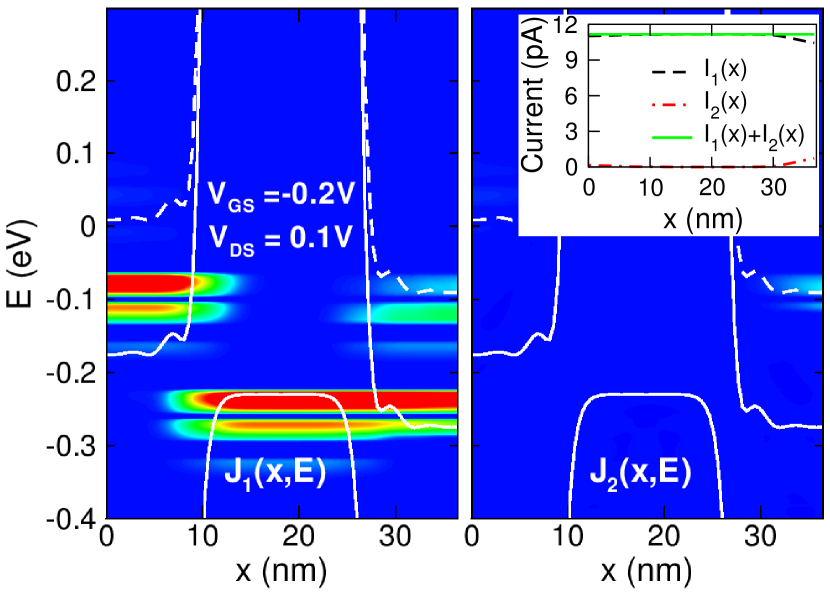
In order to test the validity of the MS method in describing inter-subband scattering, we separately plot in Fig. 4 the MS current spectrum for the first and second group of modes (corresponding to the first and second subband, respectively) at V and V, in the case with only AP scattering. It can be seen that both subbands contribute to current. In addition, despite the absence of inelastic scattering processes in the simulation, the distribution of current over energy of the single subband is not conserved when moving from source to drain, indicating that some of the carriers are transferred from one subband to the other. Indeed, thanks to phonon scattering, part of the electrons injected from the source in the second subband reach the drain by traversing the channel in the first subband, where the energy barrier is lower. The total current is properly conserved as shown in the inset of Fig. 4.
Inter-subband scattering and the conservation of the total current are also evident from simulations including OP scattering: see Fig. 5, which corresponds to a bias point where transport is dominated by phonon-assisted BTBT.
Next, we consider the TFET architecture.
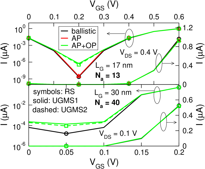
Fig. 6–top shows the vs. characteristics at V for the p-i-n counterpart of the device in Fig. 3, calculated with the different methods and by including different types of scattering, as indicated in the legend. Results obtained with both expressions MS1 and MS2 of the form-factor are reported. The symmetry of the characteristics is related to the symmetric doping of the source and drain regions Zhao et al. (2009). By looking at the RS results, one can see that AP scattering has a negligible effect in both the on- and off-state regimes, while OP scattering significantly increases the minimum leakage current and, consequently, the minimum inverse subthreshold slope (SS), similar to the n-i-n case.
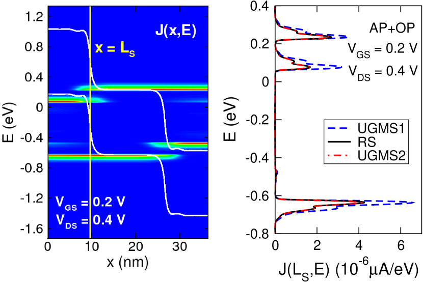
As illustrated by the current spectrum in Fig. 7–left, the increase of the minimum current is due to phonon-assisted BTBT at the source-channel and drain-channel junctions: although the first conduction and valence subbands do not face each other, electrons can transmit from the valence to the conduction subband by absorption of optical phonons. These results are in agreement with the ones in Ref. Yoon and Salahuddin, 2012.
Again, the only difference (of about a factor of ) between the RS and MS1 results is noticed in the presence of OP scattering at the point of minimum current. However, the accuracy with respect to RS can be almost completely recovered by the MS2 method, which uses the exact expression of the form-factor in (19). This is more clearly shown by the comparison in Fig. 7–right between the current spectra at the source-channel junction obtained with the different methods. The lack of accuracy of (20) in this bias condition could be related to the neglect of the terms with , which are actually of the same size as the terms included in (20). As a drawback, a slow-down of the simulation by about a factor of has been measured using MS2 compared to MS1, which can be ascribed to the increased computational cost of (18).
The above considerations apply also to the turn-on characteristics of a wider GNR TFET in Fig. 6–bottom. For this device, a lower is chosen due to the lower band gap. In addition, we set (corresponding to nm), nm, and a doping concentration in the source and drain regions of dopants/atom. 4 groups of 4 modes are used in the UGMS simulations. It is worth noticing that the UGMS method is still accurate for the wider ribbon, indicating that the decoupling in separate groups is still valid, even though the subbands are more closely spaced than in the GNR.
To evaluate the importance of the Hermitian part of , here denoted by , we report in Fig. 8
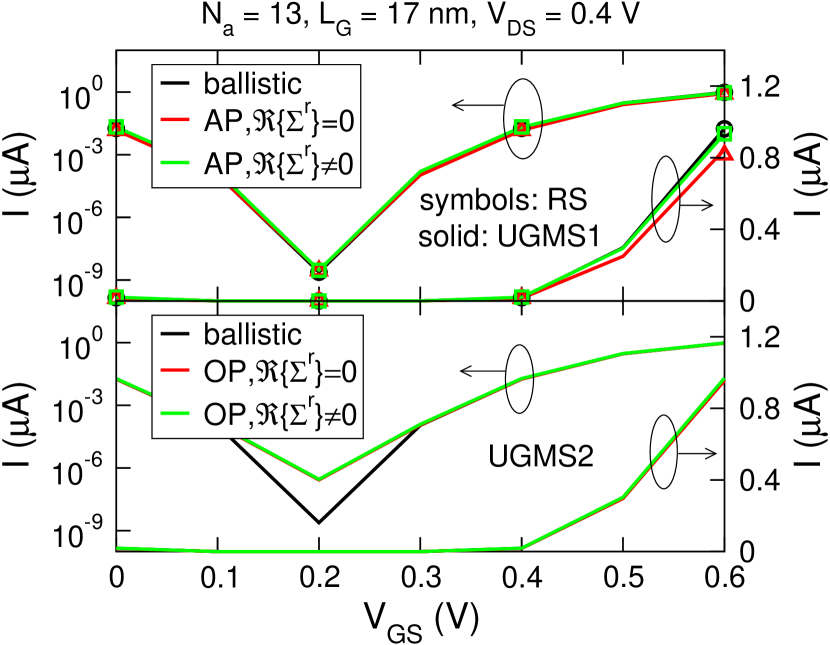
the vs. characteristics of the TFET computed with or without , separately for each type of scattering.
For AP scattering (Fig. 8–top), the neglect of leads to an underestimation of the on-state current. This can be understood as follows. In general, has the effect of shifting the Hamiltonian eigenvalues Datta (1997). However, in GNRs, the shift is of opposite sign for energies above and below the GNR mid-gap due to the symmetry of the subband structure. The result is a decrease of the GNR band gap, which favors BTBT, so that a larger current is expected when is included in the simulation. Interestingly, the two expressions of give almost identical values with respect to the minimum current. To clarify this point, we plot in Fig. 9
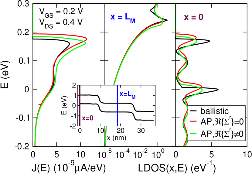
the current spectrum and the local density of states (LDOS) per slab at two positions along the device, for the bias point corresponding to the minimum current. First, it can be seen that the current spectrum with AP scattering and is larger than the ballistic one: the reason can be ascribed to an enhanced BTBT through the channel region due to the band gap narrowing effect mentioned above, which can be appreciated from the logarithmic plot of the LDOS at the mid-channel position in Fig. 9–center. Secondly, by looking at Fig. 9–right, it can be noticed that the peaks of the LDOS in the source region with are located at the same energy positions as the ones of the ballistic LDOS. On the contrary, the peaks of the LDOS with are shifted up in energy, resulting in a tunneling current larger than the ballistic one and similar to the one with (Fig. 9–left). The shift of the LDOS can be attributed to a “loss of charge” when is set to zero Svizhenko and Anantram (2005) and to the combined effect of the electrostatic feedback.
For OP scattering instead, no relevant difference is observed when including , even at high (Fig. 8–bottom).
III.2 Disordered electrostatic potential
We focus on the TFET. The simulations are performed in a non-self-consistent way, by solving the NEGF equations with a fixed electrostatic potential. We take the electrostatic potential as the sum of a disorder potential and the one calculated self-consistently in the absence of disorder and in the ballistic limit at V and V, using the RS approach. Two types of disorder are considered: a “long-range” one, i.e. slowly varying on the atomic scale, and a “short-range” one, i.e. rapidly varying from one atom to its neighbor ones. According to the first model, which is derived from Ref. Poljak et al., 2012, the disorder energy potential at the atomic site , located at position , is calculated as
| (21) |
where , , are parameters, while and are random variables: can take values with equal probability; is uniformly distributed over all the atomic position . The second model we study is the Anderson type of disorder Lherbier et al. (2008), according to which , where is a random variable uniformly distributed in .
The coherent case, i.e. without phonon scattering, is considered first.
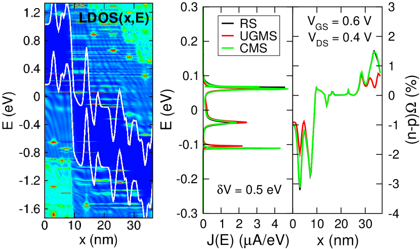
In Fig. 10–left we show the LDOS corresponding to a realization of the long-range type of disorder, obtained with , , and eV, where is the total number of carbon atoms inside the device and is the carbon-carbon bond length. The resonant states induced by disorder are clearly visible in the LDOS. In Fig. 10–center and Fig. 10–right we compare the current spectrum and net electron charge along the device, respectively, obtained with RS, UGMS, and CMS. The UGMS simulations are performed with the same 2 groups of 4 modes used in the case without disorder, while the CMS ones use the same 8 modes but all coupled in one group. It turns out that the UGSM method looses accuracy due to disorder-induced mode mixing, while the CMS method leads to results very close to the RS ones (e.g. the error on the current value is less than ).
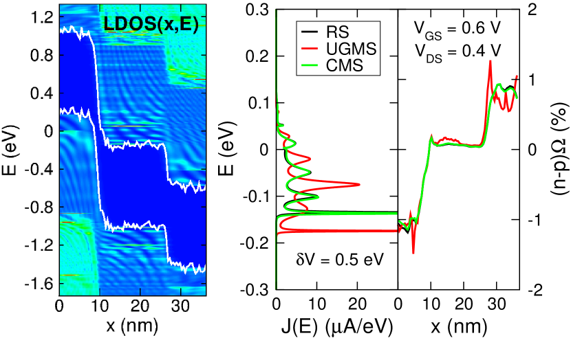
Similar considerations can be made regarding the results obtained with the second model of disorder with eV. (Fig. 11). The more regular LDOS pattern and the higher current spectrum in Fig. 11 compared to Fig. 10 indicate that the amount of scattering in this device is smaller.
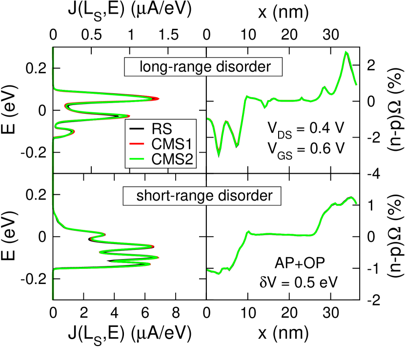
The simulations have been repeated including AP and OP scattering (Fig. 12). For both types of disorder, it is seen that the MS1 and MS2 approximations of the form-factor provide similar results and that the CMS approach is still accurate with respect to RS. By comparing the current spectra in Fig. 12 with the ones in Figs. 10–11, it can be noticed that phonon scattering adds a significant broadening. In the case of short-range disorder, phonon scattering only slightly decreases the current (from to A). On the other hand, in the case of long-range disorder, the current is increased from to A when phonon scattering is included in the simulation, indicating that the localization transport regime Datta (1997) that occurs in the coherent approximation is broken by the dephasing effect of phonon scattering.
IV Conclusions
A mode space method for TB NEGF simulations of armchair GNR FETs including phonon scattering has been presented and tested with reference to both conventional and tunnel FET structures. When no disorder is included in the simulation, an efficient decoupling of the modes in different groups (UGMS) can be employed with excellent accuracy. Despite the decoupling, the method correctly accounts for inter-subband scattering. Simplified expressions of the scattering-self energies have been compared. The one obtained by neglecting some entries of the form-factor is found to be accurate except for the bias points where transport occurs by phonon-assisted BTBT. On the other hand, the real part of the scattering self-energy has only a limited effect on the device characteristics, especially for the case of optical phonon scattering, where its calculation is most demanding. In the presence of a disorder potential, the modes need to be coupled in a single group (CMS) to account for mode mixing, but no additional modes, compared to the ones used to simulate the case without disorder, need to be included to achieve accurate results.
While the computational advantage of CMS over RS is about a constant factor with respect to the GNR width (equal to about 30 for the simulation parameters chosen in this paper), the speed-up of UGMS compared to RS is about for a device width of 1.5 nm and increases proportionally to the second power of the GNR width (for the 5-nm-wide device considered in this paper such speed-up is about ).
Acknowledgements.
R. G. would like to thank Dr. E. Baravelli of University of Bologna for fruitful discussions on the mode-space approach. This work has been supported by the EU project GRADE 317839. The authors acknowledge the CINECA Award N. HP10CPFJ69, 2011 for the availability of high performance computing resources and support.Appendix A Calculation of the retarded phonon self-energy
We consider here only the RS case, the generalization of the expressions to MS being straightforward.
Replacing (4) and (5) into the last member of (7) and using the identity analogous to (7) valid for the matrices, one can write
| (22) |
with
| (23) |
and
| (24) |
which does not contain . It is worth noticing that the principal part integral in (24) contains only a fraction of the Hermitian part of (Esposito et al., 2009). It is calculated here by means of a piecewise constant approximation of over the energy domain , which is discretized uniformly with energy steps typically of the order of , i.e.
| P | (25) | ||||
where the summation extends over all discrete energy points . An expression of analogous to (24) containing instead of can also be derived. Expression (24) is preferred for higher than the contact Fermi energies, since the numerical error introduced by truncating the upper limit of the integral to is minimized due to the decaying nature of at high energies. On the contrary, the alternative expression of which depends on is used for low energies below the contact Fermi levels, for analogous reasons. For intermediate energies an average of the two formulations is used.
References
- Han et al. (2007) M. Y. Han, B. Özyilmaz, Y. Zhang, and P. Kim, Phys. Rev. Lett. 98, 206805 (2007).
- Chen et al. (2007) Z. Chen, Y.-M. Lin, M. J. Rooks, and P. Avouris, Physica E 40, 228 (2007).
- Wang et al. (2008) X. Wang, Y. Ouyang, X. Li, H. Wang, J. Guo, and H. Dai, Phys. Rev. Lett. 100, 206803 (2008).
- Fiori and Iannaccone (2007) G. Fiori and G. Iannaccone, IEEE Electron Device Letters 28, 760 (2007).
- Ouyang et al. (2007) Y. Ouyang, Y. Yoon, and J. Guo, IEEE Trans. Electron Devices 54, 2223 (2007).
- Liang et al. (2007) G. Liang, N. Neophytou, M. S. Lundstrom, and D. E. Nikonov, J. Appl. Phys. 102, 054307 (2007).
- Yoon et al. (2008) Y. Yoon, G. Fiori, S. Hong, G. Iannaccone, and J. Guo, IEEE Trans. Electron Devices 55, 2314 (2008).
- Zhao et al. (2009) P. Zhao, J. Chauhan, and J. Guo, Nano Lett. 9, 684 (2009).
- Grassi et al. (2009) R. Grassi, A. Gnudi, E. Gnani, S. Reggiani, and G. Baccarani, J. Comput. Electronics 8, 441 (2009).
- Datta (2005) S. Datta, Quantum Transport: Atom to Transistor (Cambridge University Press, Cambridge, UK, 2005).
- Ouyang et al. (2008) Y. Ouyang, X. Wang, H. Dai, and J. Guo, Appl. Phys. Lett. 92, 243124 (2008).
- Yoon et al. (2011) Y. Yoon, D. E. Nikonov, and S. Salahuddin, Appl. Phys. Lett. 98, 203503 (2011).
- Yoon and Salahuddin (2012) Y. Yoon and S. Salahuddin, Appl. Phys. Lett. 101, 263501 (2012).
- Akhavan et al. (2012) N. D. Akhavan, G. Jolley, G. A. Umana-Membreno, J. Antoszewski, and L. Faraone, J. Appl. Phys. 112, 094505 (2012).
- Wang et al. (2004) J. Wang, E. Polizzi, and M. Lundstrom, J. Appl. Phys. 96, 2192 (2004).
- Luisier et al. (2006) M. Luisier, A. Schenk, and W. Fichtner, J. Appl. Phys. 100, 043713 (2006).
- Jin et al. (2006) S. Jin, Y. J. Park, and H. S. Min, J. Appl. Phys. 99, 123719 (2006).
- Poli (2009) S. Poli, Modelling and simulations of post–CMOS devices, Ph.D. thesis, University of Bologna (2009).
- Esposito et al. (2009) A. Esposito, M. Frey, and A. Schenk, J. Comput. Electron. 8, 336 (2009).
- Nikonov et al. (2009) D. Nikonov, H. Pal, and G. Bourianoff, “Scattering in NEGF: Made simple,” http://nanohub.org/resources/7772 (2009).
- Afzalian (2011) A. Afzalian, J. Appl. Phys. 110 110, 094517 (2011).
- Shin (2009) M. Shin, J. Appl. Phys. 106, 054505 (2009).
- Grassi et al. (2011) R. Grassi, A. Gnudi, E. Gnani, S. Reggiani, and G. Baccarani, IEEE Transactions on Nanotechnology 10, 371 (2011).
- Zhao and Guo (2009) P. Zhao and J. Guo, J. Appl. Phys. 105, 034503 (2009).
- Son et al. (2006) Y.-W. Son, M. L. Cohen, and S. G. Louie, Phys. Rev. Lett. 97, 216803 (2006).
- Lake et al. (1997) R. Lake, G. Klimeck, R. C. Bowen, and D. Jovanovic, J. Appl. Phys. 81, 7845 (1997).
- Svizhenko et al. (2002) A. Svizhenko, M. P. Anantram, T. R. Govindan, B. Biegel, and R. Venugopal, J. Appl. Phys. 91, 2343 (2002).
- Koswatta et al. (2005) S. O. Koswatta, M. S. Lundstrom, M. P. Anantram, and D. E. Nikonov, Appl. Phys. Lett. 87, 253107 (2005).
- Datta (1997) S. Datta, Electronic Transport in Mesoscopic Systems (Cambridge University Press, Cambridge, UK, 1997).
- Svizhenko and Anantram (2005) A. Svizhenko and M. P. Anantram, Phys. Rev. B 72, 085430 (2005).
- Poljak et al. (2012) M. Poljak, E. B. Song, M. Wang, T. Suligoj, and K. L. Wang, IEEE Trans. Electron Devices 59, 3231 (2012).
- Lherbier et al. (2008) A. Lherbier, B. Biel, Y.-M. Niquet, and S. Roche, Phys. Rev. Lett. 100, 036803 (2008).