Tunneling spectroscopy of phosphorus impurity atom on Ge(111)-(2x1)
surface.
Ab initio study.
Abstract
We have performed the numerical modeling of Ge(111)-(2x1) surface electronic properties in vicinity of P donor impurity atom located near the surface. We have found a notable increase of surface around surface dopant near the bottom of empty surface states band , which we called split state due to its limited spatial extent and energetic position inside the band gap. We show, that despite of well established bulk donor impurity energy level position at the very bottom of conduction band, surface donor impurity on Ge(111)-(2x1) surface might produce energy level below Fermi energy, depending on impurity atom local environment. It was demonstrated, that impurity, located in subsurface atomic layers, is visible in STM experiment on Ge(111)-(2x1) surface. The quasi-1D character of impurity image, observed in STM experiments, is confirmed by our computer simulations with a note that a few -bonded dimer rows may be affected by the presence of impurity atom.
pacs:
68.35.Dv, 68.37.Ef, 73.20.At, 73.20.HbI Introduction
At present it is a common place that Ge(111)-(2x1) surface consists of -bonded zigzag chains. This was confirmed many times by different means, see Rohlfing et al. (2000); Stekolnikov et al. (2002); Bussetti et al. (2008) and references therein. Surprisingly, just a few publications are devoted to investigations of impurity atoms on (111) surface of elemental semiconductors Garleff et al. (2007, 2005); Trappmann et al. (1997); Oberbeck et al. (2004); Arseyev et al. (2005); Schöck et al. (2000); Studer et al. (2012, 2013). And as one can see the interest to Si(111)-(2x1) surface is renewed. But not to Ge(111)-(2x1) surface. This is unexplainable, because Ge is the main candidate for technology, allowing to overcome scaling limits of Si-based MOSFETs Koike et al. (2013). The knowledge of local properties of Ge, especially caused by impurity atoms, is of vital importance. Besides, the surface and interface properties of Ge(111) have great significance for Ge spintronics applications. It is known Ge has some advantages above Si Jain et al. (2012).
The STM method till now is the only physical method achieving atomic resolution in real space. But experimenters often suffers from the lack of some reference points provided by the theory. For example, the reliable STM image interpretation still remains the challenging task. There is no general approach which takes into account all kind of physical processes responsible for STM image formation. Below we report on surface electronic structure investigation performed by ab initio computer simulations in the density functional framework, which is the first order estimation for STM/STS images, and could serve as a basis for further model improvements.
We restrict the present investigation to the case of left (negative) only surface buckling (Fig. 1(I)) as at present this matter is still controversial and is the subject of intensive investigations Violante et al. (2012); Löser et al. (2012); Bussetti et al. (2011). Our research is in some sense similar to reported in Garleff et al. (2007) for Si(111)-(2x1) surface. But we take into account all possible impurity positions in two surface bi-layers of Ge(111)-(2x1) reconstruction, and besides, our analysis is not aimed on pure STM image simulation, rather on comprehensive analyses of local density of states.
II Methods
We have performed our DFT calculations in LDA approximation as implemented in SIESTA Artacho et al. (1999) package. The use of strictly localized numerical atomic orbitals is necessary to be able to finish the modeling of large surface cell in reasonable time. The surface Ge(111)-(2x1) super-cell consists of 7x21 cells of elementary 2x1 reconstruction, each 8 Ge atomic layers thick (total 2646 atoms). Vacuum gap is chosen rather big - about 20 Å. Ge dangling bonds at the slab bottom surface are terminated with H atoms to prevent surface states formation. The geometry of the structure was fully relaxed, until atomic forces have became less then 0.003 eV/Å. More details about calculations can be found elsewhere Savinov et al. (2011).
As we have reported earlier, the atomic structure of Ge(111)-(2x1) surface is strongly disturbed in vicinity of surface defects Savinov et al. (2011, 2012). A few -bonded rows around the defect are affected. That is why the geometry relaxation has been performed with the large super-cell to keep the internally periodic for DFT images of impurity well separated. Although it is still the open question, if the defect’s images separation is sufficiently large.
At the last step of simulation the spatial distribution of Khon-Sham wave-functions and corresponding scalar field of surface electronic density of states were calculated. Because of strictly localized atomic orbitals, used in SIESTA, the special procedure of wave-functions extrapolation into the vacuum has to be used (it is also implemented in SIESTA package).
III Results
III.1 Geometry and ground state properties
In STM method the LDOS is measured above the surface, The tails of wave-functions are actually making the image. Thus in DFT calculations we are interested in the following quantity:
where are Khon-Sham eigenfunctions, is finite width smearing function, are Khon-Sham eigenvalues, and summing is evaluated at certain plane (), located a few angstroms above the surface. Here the broadening is the essential part of calculations, as we know from our experience that tunneling broadening in STM experiments on semiconductors typically amounts about 100 meV. Broadening provides the degree of smoothing, necessary to resemble experimental tunneling spectra.
At the first stage of DFT calculations the equilibrium geometry has to be established in the unit cell of Ge(111)-(2x1) reconstruction. Afterwards the unit cell is enlarged to the desired extend, the defect is introduced and the structure is relaxed again. The final step is calculation. The results are sketched in Fig 1.
The 1x1 and 2x1 surface irreducible Brillouin zones (IBZ) together with special points and directions are shown on pane (I). The right half of pane (I) contains the image correctly oriented with respect to special directions. The image corresponds to the whole 7x21 super-cell of 2x1 surface unit cells of Ge(111) surface, with P impurity atom placed at the position 1 (see below). We have to note that all figures are intensively cross-referenced, and the meaning of some notations on one figure can be better understood with another figure in mind.
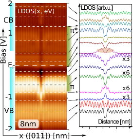
Pane Fig. 1(II) illustrates electronic structure of clean Ge(111)-(2x1) surface. Two surface states (SS) bands, empty and filled , can be seen in projected band gap. The widths of SS bands, derived from Fig. 1(II), equal to = 1.24 eV and = 0.44 eV respectively. The surface band gap is about 0.3 eV. As it should be expected, LDA approximation gives the band gap value which is much smaller than the experimental one. SS bands, as well as bulk bands, are also shown in Fig. 1(II) by small rectangles next to ordinate axis. This representation will be used on majority of figures below.
The surface band structure is presented for the case of Ge(111)-(2x1) surface with negative buckling. Our calculations predict that negative surface isomer is energetically (by almost 11 meV per (2x1) unit cell) more favorable and, as we stated above, we will restrict present analyses to negative buckling only.
The valence band (VB) top and empty SS bottom coincide with Fermi energy in Fig. 1(II). The band gap is completely covered by empty SS band. Specific for such band diagram was discussed in Arseyev et al. (2005).
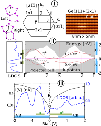
Jumping ahead, on pane Fig. 1(III) we display curve. The calculated I(V) dependence on a logarithmic scale is shown alongside. Surface curve is the result of averaging over the whole 8 nm x 5 nm area on Fig 1(I). The gap right below the Fermi level is clearly observed on graph. It does not corresponds to bulk band gap. The closest resemblance can be found with the surface band gap.
Rectangles at absсissa axis illustrate different band’s energy position. It is necessary to state, that everywhere below, the bottom of CB is schematically shown on the figures for the case of Ge(111)-(2x1) surface at room temperature. In this case the optical band gap is about 0.5 eV Olmstead and Amer (1984). The DFT band gap in LDA approximation is non-physically small, less then 100 meV. To give clear impression on relation between surface band structure and , the latter is also depicted at the left side of surface band diagram Fig. 1(II).
III.2 scalar field representation
In further exposition we will focus mostly on properties and before we go to the main results we have to clarify the physical meaning of our data representation for .
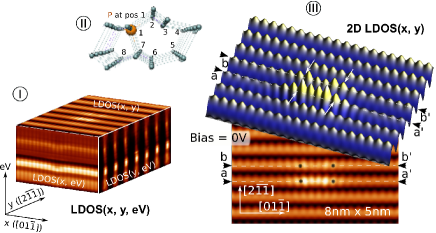
Below we are speaking about cross-sectioning of scalar field (Fig. 2(I)). The x and y directions correspond to and crystallographic directions. The two most relevant quantities are cross-section of scalar field along and planes - and respectively.
The is build up for different impurity atom positions in two subsurface bi-layers of Ge(111)-(2x1) reconstruction. The definition for donor atom position’s notation is presented in Fig. 2(II). Worth to mention, that impurity atom does not occupy exactly the same lattice site as host atom it substitutes.
In Fig. 2(III) we show the cross-sections at fixed bias voltage for the case of P donor atom located at position 1 in surface bi-layer. These images roughly correspond to experimental STM images, as at small bias voltage there are not too many sharp features, contributing to the image. It can be seen from Fig. 2, that two -bonded rows of surface reconstruction are influenced by impurity. In each row a protrusion can be observed. The spatial extent of impurity induced feature along the direction of -bonded dimer row ( direction) is at least 40 Å. Note two distinguishable maxima on the protrusion. We will come back to this fact later. Arrows and dots on the image, as well as (a-a’) and (b-b’) lines, mark spatial points and directions, referred to on figures below.
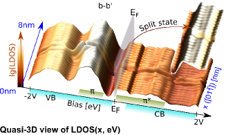
We have found notable increase of in vicinity of impurity atom at the bottom of empty SS band . We will refer to it as to split state. Fig. 3 proves the validity of this terminology. In the figure the field is shown by surfaces of equal value, colored by applied tunneling bias voltage. The is drawn for two -bonded rows denoted as a-a’ and b-b’ in Fig. 2. The position of donor atom is depicted in the figure. To prevent the confusion caused by quasi-3D picture, we clarify that the impurity is located at the left side for -bonded row b-b’, and at the right side for -bonded row a-a’.
Let us point out some important facts about this representation. First of all, high values of are confined within areas bounded by surface of constant value. They are perfectly localized above up -bonded rows. This is the reason, why only every second dimer row is imaged by STM. In between -bonded rows is relatively low. Beside this, all round shaped vertical structures in -bonded row are located above up-atom. Down-atom can be found in between them. Such spatial structure of is a consequence of collective -bonds formation. STM can only image the up-row dimers, and therefore, only up-rows. Basically, with used approach -bonds can also be directly visualized Savinov et al. (2011).
The hybridization of atomic orbitals is clearly visible from Fig. 3. It is very strong in close proximity to surface defect. This causes the appearance of specific feature near the bottom of empty SS band (marked by arrows in Fig. 2). The limited spatial and energy extents of this feature as well as its position in the band gap implies that this indeed is the split state.
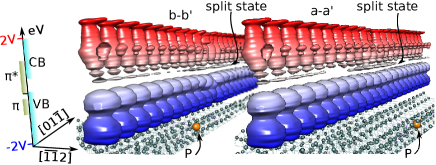
We are working with microscopic picture, on the level of individual atoms. That is why we are able to see the connection between atomic orbital’s hybridization and macroscopic band structure. Surface states itself appear due to atomic arrangement of the surface. Split state appear due to changes of this arrangement around the defect. They both have the same root - hybridization of atomic orbitals. One problem exists. It is really difficult to define the energetic position reference level, is it Fermi energy, or the SS band bottom? To be accurate we will refer to Fermi level, i.e. split state is located at the Fermi level, and not near bottom.
Axis directions and images size are indicated on the figure.
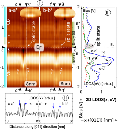
Important for our result’s understanding cross-sections at fixed coordinate are shown in Fig. 4(I). They are taken along (a-a’) and (b-b’) planes in Fig. 2, i.e. along -bonded rows of Ge(111)-(2x1) reconstruction. Areas near the Fermi level, where split state resides, are zoomed in on the insets. The positions of Fermi level , conduction band (CB) bottom, valence band (VB) top and empty and filled surface states bands are indicated in Fig. 3. According to our DFT calculations the top of VB almost coincide with the bottom of empty surface states band and Fermi level Fig. 1 and Savinov et al. (2011). Even more, the band can be partially filled at very high doping ratio Nicholls et al. (1985). Our calculations also predict for Ge(111)-(2x1) surface with negative buckling the position of empty SS band bottom about tens meV below the Fermi level.
The proportions of images are chosen on purpose in a way that is convenient for experimenters. Typically the number of point along spatial direction is less than the number of bias voltage points and tunneling spectra image is elongated in vertical direction. Though the DFT band gap in LDA approximation is non-physically small for the sake of completeness it is also shown in Fig. 4(I).
The distribution is reach of features. Its cross-section along coordinate gives the profile exactly in the same way as the cross-sectioning of (Fig. 1) along coordinate. The cross-sections of a-a’ and b-b’ panes along c-c’ line are shown on the panel (II). One can see two distinct maxima on the profiles. And what is really important is that the spatial extent of perturbation is obviously about 80 Å. The 40 Å estimation from Fig. 2 suffers from unsufficient contrast of image.
Cross-section of along coordinate (d-d’, e-e’, f-f’ and g-g’ lines Fig. 4(I)) corresponds to point spectroscopy dependencies (Fig. 4(III)) at points of profile, marked by vertical arrows in Fig. 4(II). These are points shown in Fig. 1 by dots and arrows.
Curves d-d’ and f-f’ are taken in between dimers in -bonded row, while curves e-e’ and g-g’ are taken on top of dimers (Fig. 4(II), Fig. 1). For the whole range of bias voltage the values of collected in between dimers are higher than that on top of dimers, except for narrow interval in vicinity of Fermi energy, where resides the split state. This split state contributes to the increase of on top of dimers in -bonded row. Thus, the protrusion, consisting of few dimers appear on (as well as on STM) image. It follows from Fig. 4(III) that the contrast of protrusion is higher on (a-a’) plane than on (b-b’) plane, and this indeed can be observed in Fig. 2.
To illustrate the usefulness of map the set of cross-sections along spatial coordinate is depicted in Fig 5 for P donor atom located at position 1. Profiles are slightly low pass filtered to stress the long range features, so they look a bit different comparing to Fig. 4(II). When tunneling bias changes, the profile also changes revealing depdf and protrusions of different shape. The profile, corresponding to split state energy (and to the presence of protrusion on STM image) is marked by ellipse. One can easily see that the amplitude of protrusion at Fermi level is much less than the amplitude of features at other bias voltage (see also Fig. 4(III)).
Also note, that impurity’s image might have elongated hillock like shape at positive bias (empty states). It means the protrusion on the image is not caused by charge density effects (like charge screening).
To the best of our knowledge this fact was never clearly stated. In other words, STM image of Ge(111)-(2x1) surface Arseyev et al. (2005) (as well as Si(111)-(2x1) surface Garleff et al. (2007, 2005); Trappmann et al. (1997)) around surface defect is dominated by the split state in vicinity of Fermi level, although the amplitude of the effect is relatively small.
To give even more insight into the power of data representation it is drawn in Fig. 6 as quasi-3D surface. Height is given on logarithmic scale to increase the image height contrast. The value of LDOS is coded both by height and by color with lightning. The spatial and energetic positions of specific features of tunneling spectrum can be easily deduced from the figure. The split state (zoomed in on the inset) is located at Fermi level. It has cigar like spatial shape which directly reflects in the shape of protrusion on image.
It is also obvious from Fig. 6, that split state really fills in the whole width of spectra. Thus we can not completely exclude the possibility of impurity induced electronic features overlap between neighboring super-cells of calculation. This overlap can introduce some difficult to estimate errors in quantum mechanical forces evaluation. This is the main reason, why we have increased the size of geometry relaxation surface cell to the upper available to us limit.
Let us now finish the overview of data representation. Taking stated above into account one can conclude that, given it is readily possible to estimate the outlook of point spectroscopy curves as well as the shape of spatial profiles. That is why the results of electronic properties calculations for all 8 possible positions of P impurity atom in two surface bi-layers (Fig. 2) are presented in Fig. 7 as maps.
III.3 Surface around P donor impurity
Let us point out the most important features of calculated images.
As we have discussed earlier, the empty surface states band is governing STM image formation for Ge(111)-(2x1) surface Arseyev et al. (2005, 2007) in the band gap region. Now the same concerns the split state. The STM image is dominated by split state in vicinity of Fermi energy.
The noticeable influence of surface states inside CB and VB bands can be inferred from Fig. 7. There are peculiarities near the top of empty surface states band and at the edges of filled surface states band . They are imaged as horizontal bright stripes.
For all P doping atom positions except position 3, the split state is located at the Fermi level. When P impurity is placed at position 3, the split state can be observed below Fermi energy Fig. 7(3). Position 2 is somewhat specific. In this case the impurity atom is directly breaking -bonded chain, and this strongly influences (Fig. 7(2)) - at almost all possible bias voltage values the impurity LDOS image has two well pronounced peaks.
As with other semiconductors, individual impurity is visible in STM experiment when it is located below the Ge(111)-(2x1) surface (Fig 7(5-8)). To the best of our knowledge we report this for the first time. Albeit it should be rather obvious from simple speculations. The crystal lattice is disturbed noticeable far from atomic size defect Savinov et al. (2012), and this disturb the perfectness of collective -bonding in a few dimer rows. There is also another possibility. The P is shallow impurity in Ge, its ionization energy is 13 meV. Therefore it localization radii should be large, in 50 Å range. The , observed by STM for Ge(111)-(2x1) surface must have, in particular, two contributions. One quasi-1D, coming from surface reconstruction, and another one, coming from ionized donors with large localization radii. These two contributions are superimposed on each other. The resulting STM image would be linear structure, caused by (2x1) reconstruction, with wide spots, originating from impurities. These spots are poorly visible because of perfect screening by -bonded electrons, but some influence should exist. The calculations for impurity deep below the surface are to be done in the future and there is need to re-analyze experimental data thinking in this direction. Also we should mention, that the above speculations must be taken with great care, as the common sense might often be misleading in surface physics.
The overall behavior of impurity images strongly differs, depending on the position of donor atom in the crystal cell. This is observed even for subsurface defects. The same P donor impurity may looks as protrusion, depression, protrusion superimposed on a depression etc. It depends both on the spatial location of impurity and applied bias voltage.
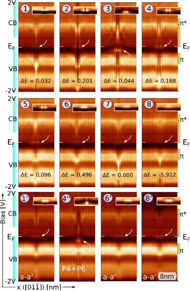
(1’, 6’, 8’) maps along a-a’ dimer row for the case when two -bonded rows are disturbed by impurity atom. (4”) map for the case of two donor atoms located at positions 4 and 6. Note split state located below Fermi level. Axis directions and images size are indicated near the bottom of the figure.
The atomic orbitals in vicinity of surface defects are strongly hybridized. This results in up/downward band edges ”bending”. The insets of Fig. 7 with split state areas zoomed in with high contrast, illustrate this. Basically, the orbital’s hybridization leads to specific spatial shape of tunneling spectra and, in other words, to the appearance of local electronic density spatial oscillations Savinov et al. (2011, 2012). Let us note, these are not charge density oscillations, because they are observed in empty states energy range (above Fermi level). Spatial oscillation on Ge(111)-(2x1) surface were the subject of Muzychenko et al. (2010) work.
The energy differences, measured with respect to the total energy of a system of 2646 atoms with P donor atom at position 7, are shown on every pane of Fig. 7. The difference is not very large. At least, we suppose, it does not allow to make any conclusions about the most favorable position of donor atom. The difference is large for donor positions 8. We do not have any explanation for huge energy gain for impurity position 8. At the same time this energy difference applies to the huge surface slab. Due to slightly different atoms relaxation a few electronvolts can easily be acquired by the whole super-cell. Also it could be, that the thickness of model slab is not sufficient.
The last row of Fig. 7 will be described later on.
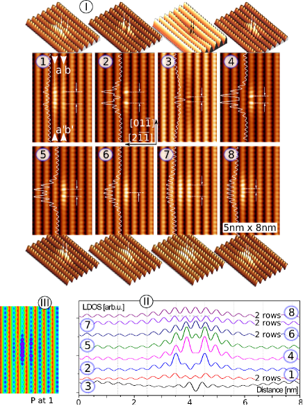
The (and STM) image of individual impurity is dominated by the split state at zero (Fig. 1) and low bias (see above) voltage as illustrated by Fig. 8, where zero bias maps of for different donor atom positions are presented together with corresponding quasi-3D images. The profiles along b-b’ direction (the same for Fig. 2 and Fig. 8) are shown on the maps with equal scales.
Three things can be immediately noticed from Fig. 8. Firstly, one or two -bonded rows are affected by donor impurity. Secondly, one or two local maxima are present on the profile. Thirdly, the distance between maxima can be one or two dimers along -bonded row ([01] direction). This is shown in Fig. 8 by thin lines and arrows and is summarized in Table. 1.
| Atom position | 1 | 2 | 3 | 4 | 5 | 6 | 7 | 8 | |
|---|---|---|---|---|---|---|---|---|---|
| 2 rows | x | - | - | - | - | x | x | x | |
| 2 maxima | x | x | x | x | x | - | x | x | |
| Num. dimers | 2 | 2 | 1 | 1 | 1 | - | 2 | 1 |
Thus, P donor impurity at position 1 is imaged as two row feature with two maxima in a row and double dimer distance between maxima.
To be absolutely accurate, not two, but a few rows are affected by impurity. The situation is the same as with spatial extent of image protrusion. One should either increase the contrast of images (see Fig. 8(III)), either use profiles in analyses (Fig. 8(II)). Reduction to two disturbed rows allows to classify images of impurity located at different positions.
Having this classification, we can apply it to the test case. Si(111)-(2x1) and Ge(111)-(2x1) surfaces are similar in many senses. It is possible to perform a simple check of our results by comparison with Si(111)-(2x1) surface Garleff et al. (2007). In general the situation with STM imaging of individual impurities is much more simple on Si(111)-(2x1) surface. The empty surface states band and the valence band VB are separated by about 0.4 eV gap Löser et al. (2012). Near Fermi level there are no states, available for tunneling, but empty surface states. That is why the STM impurity images on Si(111)-(2x1) are much easier to classify.
In accordance with Fig. 8 and Table. 1 the conclusions of authors can be immediately confirmed. In our notations: Fig.2a Garleff et al. (2007) corresponds to P in position 2, Fig.2b Garleff et al. (2007) - P in position 4, Fig.2b Garleff et al. (2007) - P in position 5. The remaining unclear feature (Fig.2d Garleff et al. (2007) ) most probably is the STM image of P atom, adsorbed on the surface. This statement is out of scope of present investigation and will be proved in the future publications Savinov et al. .
Now we can come back to the lowest row of Fig. 7. Images 1’, 6’ and 8’ correspond to cross-sections of scalar field along a-a’ plane (see Fig. 2), i.e. along second (along with b-b’) disturbed -bonded row. As it can be seen from Fig. 7 the split state is also present on these images (see also Fig. 3). Images 6’ and 8’ are similar with the main difference being the image contrast. image for the case of P donor placed at position 7 is not shown as maps along a-a’ and b-b’ dimer rows are almost identical. At the same time for other cases the difference between a-a’ and b-b’ maps is rather big.
The only exceptional case among 1-8 images is the case of impurity at position 3, when the split state goes below Fermi level. To check if this situation can be reproduced with slightly different atomic environment, we have performed calculations for two impurities located at different positions in the atomic lattice. First impurity was fixed at position 6, while the second was sequentially placed at positions from 1 to 4. The results for P4-P6 pair is depicted in Fig. 7(4”). One can see that split state for impurity at position 4 was shifted below Fermi level by adding second impurity to position 6. Thus we proved, that split state location below Fermi energy can be observed for different conditions. The comprehensive analyses of donor pairs is out of scope of current paper.
III.4 Local tunneling spectroscopy
The last problem we would like to discuss is the local spectroscopy curves. This article was written with experimenter’s needs in mind, so we will analyze spectroscopy curves as if they were obtained by STM. There are two approaches to measure the tunneling spectra. One is simple I(V) curve measurement at certain surface point. It heavily relies on very high stability of mechanical system. Basically this is a case last years. Another approach is based on averaging of I(V) curves above some surface area. It is less sensitive to different noise.
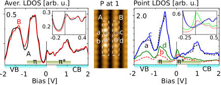
The problem is that two approaches can give different from the first sight results. In Fig. 9 we present model tunneling spectra for different measurement conditions for the case of P atom located at site 1. On the left pane there are spectra averaged over A and B areas above -bonded rows. On the right pane spectroscopy curves at points a, b, c and d are depicted. Points b and d are located on top of dimers in a row. Points a and c are in between dimers. Curves A and B are almost undistinguishable, though the heights of protrusions along a-a’ and b-b’ lines (see also Fig. 2) on image strongly differ. Split state is located close to the Fermi level and this part of spectrum is zoomed in on the inset. The difference in averaged spectra is on a few percent scale, which apparently is not enough to draw any reliable conclusions. Note nonzero tunneling conductivity at Fermi energy.
As to point spectroscopy, we can easily discriminate atomic size features. Dimers at similar positions in different dimer rows give different tunneling spectra (right pane of Fig. 9). Even relatively small difference above elevated features along dimer rows is obvious.
Looking at the spectra obtained by different methods we can conclude, that point spectroscopy does not give immediate impression on the band structure, while spectroscopy with averaging does. Averaging of two point spectroscopy curves, one on top of dimer and another in between dimers, will give curve, similar to averaged spectroscopy curve. Also note the vertical scales on both panes. Averaging significantly decreases the maximum value.
There are no obvious specific points on numerical tunneling conductivity I(V) dependence (nor on its derivative) allowing simple determination of band gap edges (see Fig. 1(III)). I.e. having perfectly defined I(V) and knowing we can not determine the band gap, although this can be caused by very narrow DFT band gap.
Another conclusion that can drawn from local spectroscopy analyses is that it is almost impossible to identify individual impurity on Ge(111)-(2x1) surface relying only on the results of local spectroscopy. As we discussed earlier, the maps of should be used together with local spectroscopy data Arseev et al. (2002); Savinov et al. (2011).
III.5 Model’s limitations
Let us specify the strong assumptions used in present calculations. Some of them are imposed by very big simulation super-cell.
In particular, we have performed the simulation in LDA approximation. It is known it gives non-physically small values of band gaps. This can be slightly improved by the GGA approximation, but real improvements can be achieved only with computationally expensive GW many body corrections Violante et al. (2012). At the same time cheap ”scissors“ method works quite well Bussetti et al. (2011).
There is no correction for closed STM feedback loop. The values of are calculated on the plane above the surface.
There is no STM tip density of states in our results.
In our model we can not account for the surface band bending. We simply do not have sufficiently thick model slab. Our slab is about 15 Å thick, and the depletion layer at Ge(111)-(2x1) surface with n-type of bulk conductivity is almost 250 Å thick. The depletion layer strongly affects the picture of tunneling for n-type doped Ge samples Arseyev et al. (2005). The same concerns the Si(111)-(2x1) surface.
That is why our model STM images do not coincide exactly with experimental observations, but nevertheless the correspondence is reasonable. All maps (except position 3) predicts the presence of protrusion on the STM images at zero (and small) bias voltage, which indeed agree with experiment Savinov et al. . We did not find any substantial difference when explicitly adding charge to the impurity atom.
IV Conclusions
In conclusion, we have performed the numerical modeling of Ge(111)-(2x1) surface electronic properties in vicinity of P donor impurity atom located near the surface. We have found a notable increase of surface around surface dopant near the bottom of empty surface states band , which we called split state due to its limited spatial extent and energetic position inside the band gap. We show, that despite of well established bulk donor impurity energy level position at the very bottom of conduction band, surface donor impurity on Ge(111)-(2x1) surface might produce energy level below Fermi energy, depending on impurity atom local environment. It was demonstrated, that impurity, located in subsurface atomic layers, is visible in STM experiment on Ge(111)-(2x1) surface. The quasi-1D character of impurity image, observed in STM experiments, is confirmed by our computer simulations with a note that a few -bonded dimer rows may be affected by the presence of impurity atom.
More work is needed to clarify if deep subsurface impurity atoms will be visible for STM on Ge(111)-(2x1) surface and to investigate how the different surface isomers will affect STM images of individual impurity.
Acknowledgements.
This work has been supported by RFBR grants and computing facilities of Moscow State University. We would also like to thank the authors of WxSM and Chimera free software.References
- Rohlfing et al. (2000) M. Rohlfing, M. Palummo, G. Onida, and R. Del Sole, Phys. Rev. Lett. 85, 5440 (2000).
- Stekolnikov et al. (2002) A. A. Stekolnikov, J. Furthmüller, and F. Bechstedt, Phys. Rev. B 65, 115318 (2002).
- Bussetti et al. (2008) G. Bussetti, C. Goletti, P. Chiaradia, M. Rohlfing, M. Betti, F. Bussolotti, S. Cirilli, C. Mariani, and A. Kanjilal, Surface Science 602, 1423 (2008).
- Garleff et al. (2007) J. K. Garleff, M. Wenderoth, R. G. Ulbrich, C. Sürgers, H. v. Löhneysen, and M. Rohlfing, Phys. Rev. B 76, 125322 (2007).
- Garleff et al. (2005) J. K. Garleff, M. Wenderoth, R. G. Ulbrich, C. Sürgers, and H. v. Löhneysen, Phys. Rev. B 72, 073406 (2005).
- Trappmann et al. (1997) T. Trappmann, C. Sürgers, and H. Löhneysen, EPL (Europhysics Letters) 38, 177 (1997).
- Oberbeck et al. (2004) L. Oberbeck, N. Curson, T. Hallam, M. Simmons, and R. Clark, Thin Solid Films 464–465, 23 (2004), proceedings of the 7th International Symposium on Atomically Controlled Surfaces, Interfaces and Nanostructures.
- Arseyev et al. (2005) P. Arseyev, N. Maslova, V. Panov, S. Savinov, and C. Haesendonck, JETP Letters 82, 279 (2005).
- Schöck et al. (2000) M. Schöck, C. Sürgers, and H. v. Löhneysen, Phys. Rev. B 61, 7622 (2000).
- Studer et al. (2012) P. Studer, V. Brázdová, S. R. Schofield, D. R. Bowler, C. F. Hirjibehedin, and N. J. Curson, ACS Nano 6, 10456 (2012), http://pubs.acs.org/doi/pdf/10.1021/nn3039484 .
- Studer et al. (2013) P. Studer, S. R. Schofield, C. F. Hirjibehedin, and N. J. Curson, Applied Physics Letters 102, 012107 (2013).
- Koike et al. (2013) M. Koike, E. Shikoh, Y. Ando, T. Shinjo, S. Yamada, K. Hamaya, , and M. Shiraishi, Applied Physics Express , 23011 (2013).
- Jain et al. (2012) A. Jain, C. Vergnaud, J. Peiro, J. C. L. Breton, E. Prestat, L. Louahadj, C. Portemont, C. Ducruet, V. Baltz, A. Marty, A. Barski, P. Bayle-Guillemaud, L. Vila, J.-P. Attané, E. Augendre, H. Jaffrès, J.-M. George, and M. Jamet, Applied Physics Letters 101, 022402 (2012).
- Violante et al. (2012) C. Violante, A. Mosca Conte, F. Bechstedt, and O. Pulci, Phys. Rev. B 86, 245313 (2012).
- Löser et al. (2012) K. Löser, M. Wenderoth, T. K. A. Spaeth, J. K. Garleff, R. G. Ulbrich, M. Pötter, and M. Rohlfing, Phys. Rev. B 86, 085303 (2012).
- Bussetti et al. (2011) G. Bussetti, B. Bonanni, S. Cirilli, A. Violante, M. Russo, C. Goletti, P. Chiaradia, O. Pulci, M. Palummo, R. Del Sole, P. Gargiani, M. G. Betti, C. Mariani, R. M. Feenstra, G. Meyer, and K. H. Rieder, Phys. Rev. Lett. 106, 067601 (2011).
- Artacho et al. (1999) E. Artacho, D. Sánchez-Portal, P. Ordejón, A. García, and J. M. Soler, physica status solidi (b) 215, 809 (1999).
- Savinov et al. (2011) S. Savinov, S. Oreshkin, and N. Maslova, JETP Letters 93, 521 (2011).
- Savinov et al. (2012) S. Savinov, A. Oreshkin, and S. Oreshkin, JETP Letters 96, 31 (2012).
- Olmstead and Amer (1984) M. A. Olmstead and N. M. Amer, Phys. Rev. B 29, 7048 (1984).
- Nicholls et al. (1985) J. M. Nicholls, P. Mårtensson, and G. V. Hansson, Phys. Rev. Lett. 54, 2363 (1985).
- Arseyev et al. (2007) P. Arseyev, N. Maslova, V. Panov, S. Savinov, and C. Haesendonck, JETP Letters 85, 277 (2007).
- Muzychenko et al. (2010) D. A. Muzychenko, S. V. Savinov, V. N. Mantsevich, N. S. Maslova, V. I. Panov, K. Schouteden, and C. Van Haesendonck, Phys. Rev. B 81, 035313 (2010).
- (24) S. V. Savinov et al., To be published .
- Arseev et al. (2002) P. Arseev, N. Maslova, V. Panov, and S. Savinov, Journal of Experimental and Theoretical Physics 94, 191 (2002).