Intrinsic Electrical Transport Properties of Monolayer Silicene and MoS2 from First Principles
Abstract
The electron-phonon interaction and related transport properties are investigated in monolayer silicene and MoS2 by using a density functional theory calculation combined with a full-band Monte Carlo analysis. In the case of silicene, the results illustrate that the out-of-plane acoustic phonon mode may play the dominant role unlike its close relative graphene. The small energy of this phonon mode, originating from the weak sp2 bonding between Si atoms, contributes to the high scattering rate and significant degradation in electron transport. In MoS2, the longitudinal acoustic phonons show the strongest interaction with electrons. The key factor in this material appears to be the Q valleys located between the and K points in the first Brillouin zone as they introduce additional intervalley scattering. The analysis also reveals the potential impact of extrinsic screening by other carriers and/or adjacent materials. Subsequent decrease in the actual scattering rate can be drastic, warranting careful consideration. Finally, the effective deformation potential constants are extracted for all relevant intrinsic electron-phonon scattering processes in both materials.
pacs:
71.15.Mb, 72.10.Di, 72.20.Ht, 73.50.DnI INTRODUCTION
Very recently, the attention to low-dimensional materials has expanded beyond the best known example of this kind graphene. Novoselov2005MoS2 ; Wang2012_2D ; Coleman2011 ; Sahin2009 In particular, silicene Kara2012 ; Cahangirov2009 ; Vogt2012 and molybdenum disulfide Mak2010 ; Radisavljevic2011 ; Kim2012 ; Kong2012 have gained much interest due to their unique properties in electronics, optoelectronics and magnetics. Silicene is expected to share certain superior properties of graphene due to its structural similarity and the close position in the periodic table. More importantly, it is compatible with the current silicon-based technology and can be grown on a number of different substrates. Chen2012_Silicene ; Feng2012 ; Fleurence2012 On the other hand, atomically thin MoS2 is a semiconductor with a finite band gap that ranges from approximately 1.3 eV to 1.9 eV depending on the thickness. Mak2010 It has been used as the channel material in field effect transistors with promising results. Radisavljevic2011 ; Lembke2012 In addition, monolayer MoS2 offers the possibilities of interesting spin and valley physics utilizing the strong spin-orbit coupling. Xiao2012 ; Cao2012 ; Zeng2012 ; Mak2012
Characterization of electronic transport, particularly the intrinsic properties, is critical for assessing and understanding the potential significance of a material. In the case of silicene, many of the crucial parameters are presently unknown due to the brief history of this material. In comparison, notable advances have been made in MoS2 lately. Experimental investigation of transistor characteristics deduced the channel mobilities ranging from 200 cm2/Vs to 1000 cm2/Vs at room temperature, Radisavljevic2011 ; Lembke2012 while a theoretical study estimated an intrinsic phonon-limited value of 410 cm2/Vs based on a first-principles calculation of electron-phonon interaction. Kaasbjerg2012 However, questions remain regarding the intrinsic electron transport in MoS2. For instance, those extracted from transistor current-voltage (I-V) measurements are indirect accounts and can be strongly affected by extrinsic factors. Similarly, the latter work Kaasbjerg2012 includes only the electronic states in the conduction band minima at the K points in the first Brillouin zone (FBZ); the impact of Q valleys located along the -K symmetry directions (which correspond to the minima of bulk MoS2) were not considered. A detailed investigation is clearly called for.
In this paper, we examine intrinsic transport properties of monolayer silicene and MoS2 by taking advantage of first-principles analysis and full-band Monte Carlo simulation. Along with the electronic band structure, the phonon spectra and electron-phonon coupling matrix elements are calculated for all phonon branches within the density functional theory (DFT) formalism. Baroni2001 ; Borysenko2010 The obtained electron scattering rates are subsequently used in the Boltzmann transport equation to compute the intrinsic velocity-field characteristics with a full-band Monte Carlo treatment. The calculation results are compared with the available data in the literature and the key factors affecting electron transport in these materials elucidated. The investigation also provides the effective deformation potential constants extracted from the first-principles results.
II THEORETICAL MODEL
Both monolayer silicene and MoS2 are hexagonal crystals. To account for their delicate atomic structures accurately, the calculations are performed in the DFT framework, as it is implemented in the QUANTUM-ESPRESSO package, (Giannozzi2009, ) using ultrasoft pseudopotentials. A minimum of 35 Ry is used for the energy cut-off in the plane wave expansion along with the charge truncation 15 times larger. The generalized gradient approximation is used for the exchange-correlation potential for silicene, while the local density approximation is adopted for MoS2. The momentum space is sampled on a 36361 Monkhorst-Pack grid with no offset (silicene) or on a 18181 grid (MoS2) for electronic band calculation. The simulated cells are optimized in both cases until the atomic forces decrease to values less than 0.015 eV/Å.
Each phonon is treated as a perturbation of the self-consistent potential, created by all electrons and ions of the system, within the linear response [i.e., density functional perturbation theory (DFPT)]. Baroni2001 The calculation of the potential change due to this perturbation gives the value of the electron-phonon interaction matrix element: Borysenko2010
| (1) |
where is the Bloch electron eigenstate with the wavevector , band index , and energy ; is the derivative of the self-consistent Kohn-Sham potential Baroni2001 with respect to atomic displacement associated with the phonon from branch with the wavevector and frequency ; and M is the atomic mass. Numerical calculations of lattice dynamics are conducted on a 18181 Monkhorst-Pack grid. Indices are dropped hereinafter as only the first (lowest) conduction band is considered.
With the electron-phonon interaction matrix from the first-principles calculation, the scattering rate of an electron at state can be obtained by using Fermi’s golden rule,
| (2) |
where is the phonon occupation number, the Boltzmann constant, and the temperature. As we are interested in the intrinsic scattering probability that is not limited to a specific carrier distribution (and thus, the Fermi level), our formulation assumes that all final electronic states are available for transition (i.e., nondegenerate) in the bands under consideration.
For transport properties, a Monte Carlo approach with full-band treatment is adopted. All of the details described above, including the wavevector (,) dependence of the scattering matrix elements [e.g., Eq. (1)], are accounted for. This allows solution of the Boltzmann transport equation beyond the conventional relaxation time approximation.
III RESULTS AND DISCUSSION
III.1 Monolayer Silicene
Earlier first-principles studies have shown that the stable structure for monolayer silicene has a low-buckled configuration. Sahin2009 ; Cahangirov2009 While planar and high-buckled cases lead to imaginary phonon frequencies around the point indicating an unstable structure, the low-buckled construction provides well separated phonon branches and positive frequencies. The origin of buckled geometry in silicene is the weakened bonding of the electrons in the outer shell. Compared with graphene, which has very strong bonding and planar geometry, the interatomic bonding distance is much larger in silicene, which decreases the overlap of orbitals and dehybridizes the states. Accordingly, the planar geometry cannot be maintained. In our analysis, the lattice constant is optimized to be 3.87 Å, with the buckling distance of 0.44 Å, in good agreement with Ref. Sahin2009, .
Figure 1 shows the outcome of electronic and phononic band calculation in monolayer silicene. The Fermi velocity extracted from the Dirac cone is around cm/s that is roughly one half of that in graphene [see bands and in Fig. 1(a)]. While this result is in agreement with other theoretical predictions, Cheng2011 ; Drummond2012 a value as high as cm/s was also claimed in the literature. Cahangirov2009 As for phonons in Fig. 1(b), six branches are identified with two atoms per unit cell. The transverse acoustic (TA) and longitudinal acoustic (LA) phonon dispersion relations are well approximated by sound velocities in the long-wavelength limit; cm/s and cm/s. Although the out-of-plane acoustic (ZA) phonon exhibits an approximate q2 dependence near the center of the Brillouin zone, its sound velocity can also be estimated; cm/s. An interesting point to note in the phonon dispersion is the discontinuities in the frequency derivative of the highest optical branch that, similar to graphene, appear at the high symmetry points, and K. These discontinuities are referred to as Kohn anomalies, Piscanec2004 ; Cheng2011 induced by unusual screening of lattice vibrations by conduction electrons. Sharp cusps typically indicate strong electron-phonon coupling. Calculated phonon energies at the , M, and K points in the FBZ are summarized in Table LABEL:table_ph_Silicene.
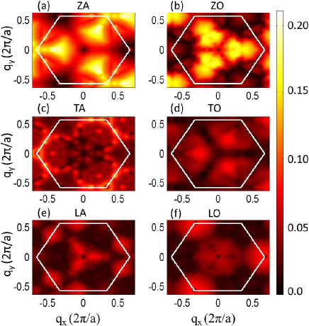
The electron-phonon interaction matrix elements obtained for the electron at the Dirac point [i.e., ] are plotted in Fig. 2 as a function of phonon wavevector . Kohn anomalies, illustrated by the three peaks at three equivalent K points in the transverse optical (TO) mode and another at the zone center for the longitudinal optical (LO) branch, are not as distinct as those observed in graphene. Borysenko2010 Overall, coupling of optical phonons with electrons appears to be relatively weak. In comparison, the acoustic phonons show much stronger interaction. Particularly striking is the large strength of ZA phonon coupling, unlike in graphene. Due to the buckled geometry (originating from the weak bonding mentioned earlier), silicene does not maintain certain key characteristics of ideal planar lattice, especially the reflection symmetry with respect to the atomic plane. As such, the symmetry consideration, in which only the in-plane phonons can couple linearly to two-dimensional (2D) electrons, Manes2007 no longer applies. An increased role of ZA phonons is clearly expected.
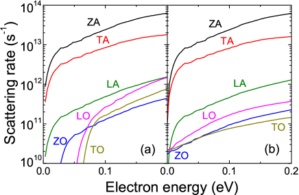
The scattering rates calculated at room temperature ( K) are shown in Fig. 3. The result is plotted specifically for electrons with wavevector along the K- direction. Since the integration in Eq. (2) is over the entire FBZ, both intravalley () and intervalley () transition events are included. As the interaction matrix elements illustrated above suggest, acoustic phonons have much larger scattering rates than optical modes. Specifically, the ZA branch provides the dominant contribution, which can be attributed to the observed large coupling strength as well as the small phonon energy near the zone center (i.e., a large occupation number ). This also indicates that the scattering rates are very sensitive to the phonon energies (or equivalently the value of ). Since an accurate description of ZA dispersion in the long wavelength limit requires a well converged calculation with a sufficiently dense grid, care must be taken when evaluating accuracy of the data in the literature. Drummond2012 ; Cahangirov2009
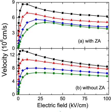
Figure 4(a) provides the drift velocity versus electric field at different temperatures obtained by full-band Monte Carlo simulations. The intrinsic mobility estimated from the figure is approximately 1200 cm2/Vs and the saturation velocity (defined at 100 kV/cm) cm/s at 300 K. When the temperature decreases, both the mobility and the saturation velocity enhance due to the suppression of phonon excitation; the respective values at 50 K are 3.0104 cm2/Vs and cm/s. The drift velocities show a slight negative slope at high fields that becomes more pronounced at low temperatures. This phenomenon (i.e., the negative differential resistance) can be explained, at least in part, by the nonlinear band dispersion at high electron energies as in graphene. Li2011
The calculation results discussed above demonstrate the intrinsic properties of silicene. When this material is synthesized or placed on a substrate, however, additional scattering sources such as surface polar phonons and impurities must be considered, which could degrade the performance further. A topic that may need additional attention is the role of ZA phonons in the presence of a supporting material. As recent measurement of graphene in-plane thermal conductivity attests, Cai2010 even a weak binding between a 2D crystal and the substrate could dampen the ZA vibrations substantially. Moreover, it is reasonable to anticipate that the extent of this suppression would be dependent on the detailed interaction between two materials. Since ZA phonons provide the dominant role in the electron-phonon interaction in silicene, it (i.e., the damped vibration) could actually lead to sizable reduction in the scattering rate. To gauge the impact, transport characteristics are also studied without the ZA scattering. As shown in Fig. 4(b), the mobility experiences an increase of greater than threefold (3900 cm/s), while the saturation velocity goes up more modestly ( cm/s). This estimate may be considered an upper limit for silicene on a substrate.
III.2 Monolayer MoS2
In the present DFT calculation for monolayer MoS2, the optimized lattice constant is 3.13 Å, consistent with other theoretical studies. Kadantsev2012 ; Kaasbjerg2012 ; Molina2011 Furthermore, this value is in good agreement with Å determined experimentally in bulk MoS2. Wakabayhi1975 The resulting electronic and phononic band dispersion is depicted in Fig. 5. As shown, monolayer MoS2 is a semiconductor with a direct gap of 1.86 eV at the K point a number within a few percent from a recent measurement of 1.9 eV. Mak2010 Our calculation also predicts the presence of second energy minima only about 70 meV higher. These so-called Q valleys are located along the -K axes at approximately the half-way points [e.g., Q= vs. K=]. At present, the energy separation between the K and Q valleys is unsettled with the estimates ranging from 50 meV to 200 meV. Kadantsev2012 ; Kaasbjerg2012 Since this is a crucial parameter for electron transport, a more extended discussion is provided later in the paper in relation to intervalley scattering. The band dispersion relations around the energy minima are nearly quadratic and can be well described by the effective mass approximation. For the K valleys (i.e., the energy minima at the equivalent K points), the extracted longitudinal and transverse effective masses are almost identical, . On the other hand, the Q valleys yield , with the longitudinal direction defined along the -K axis. denotes the electron rest mass.
Monolayer MoS2 has the symmetry of the point group , with nine branches of phonons. The irreducible representations associated with each phonon mode, together with the polarization (longitudinal or transverse), help denote all of the vibrational modes, Molina2011 ; Lee2010 as plotted in Fig. 5. The E′′ modes are degenerate at the point. These two modes are the in-plane optical vibrations, with two S atoms moving out of phase and Mo atom static. The E′ modes are polar LO and TO phonons, with Mo atom and two S atoms moving out of phase. Due to the coupling with the macroscopic electric field, there is LO-TO separation at the point, which slightly lifts the LO(E′) mode upward on energy scale. A non-analytical part is added to the dynamic matrix resulting in a small splitting of about 0.3 meV [not visible due to the energy scale of Fig. 5(b)]. The A1 and A branches are two out-of-plane optical phonon modes. A1 is also referred to as the homopolar mode, with two S atoms moving out of phase and Mo atom static. In the A mode, Mo atom and two S atoms vibrate out of phase. The three lowest branches are LA, TA, and ZA modes, with sound velocities of cm/s, cm/s. The phonon energies at different symmetric points are summarized in Table LABEL:table_ph_MoS2.
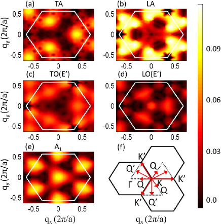
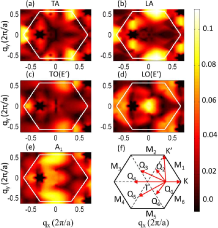
Figures 6 and 7 show the electron-phonon interaction matrix elements for the initial electron state at [=] and [ ], respectively, for TA, LA, TO(E′), LO(E′), and A1 (or homopolar) phonon modes. The contribution from the remaining four branches is found to be negligible due to the weak coupling. The matrix elements for demonstrate a threefold rotational symmetry (i.e., 120∘), while those of show the reflection symmetry with respect to the axis. As expected, the LO(E′) phonons near the point possess the characteristics of Fröhlich coupling through the induced macroscopic electric field typical of polar materials. Since the relative electronic potential is not periodic in the long wavelength limit, Baroni2001 DFPT does not yield a correct value to the electron-phonon interaction matrix. For an approximation, the matrix element of LO(E′) is interpolated at by using the values from the nearby points. This [i.e., LO(E′)] and A1 are the only two modes that have non-zero scattering matrix as (intravalley scattering); in the other three branches, the matrix elements only have first-order components, , leading to . With regard to intervalley scattering that requires large phonons, a number of different transition processes are possible as shown in Figs. 6(f) and 7(f). For instance, Fig. 6 indicates strong electron-phonon interaction at the symmetry points M in the phonon momentum space (denoted as for simplicity) for all modes except LO(E′); these phonons can induce electron transition from K to Q′ valleys. Another example is the phonons at for all five modes in Fig. 7, which can be associated with electron scattering from to .
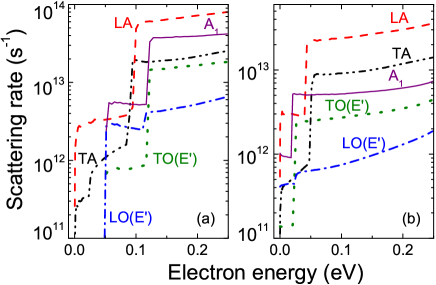
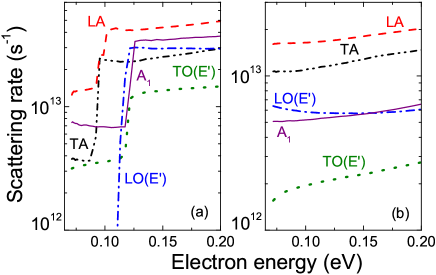
The electron-phonon scattering rates are calculated as a function of electron energy using Fermi’s golden rule. Figure 8 gives the rates for electrons in the K valleys at room temperature, while the result for Q-valley electrons is shown in Fig. 9. Similarly to silicene, the wavevector of the initial electronic state is chosen along the K- or Q- axis, respectively. As can be seen from the figures, the LA mode provides the largest scattering rates consistent with its large coupling strength. The discontinuities or steps in the curves represent either the onset of optical phonon emission or intervalley scattering. For instance, the abrupt increase observed in the rate of LA phonons at 100 meV in Fig. 8(a) can be attributed to the above mentioned strong transition via emission of a LA phonon with . Since this phonon energy is approximately 30 meV (see Fig. 5), the final state energy of 70 meV indeed matches to the Q-K separation . Similarly, the onset of transition via absorption can be found around 40 meV in Fig. 8(b). The large density of states in the Q valleys (evident from the large effective masses) makes the contribution of this scattering even more prominent. If, on the other hand, all of the final states in the Q valleys are excluded, the total scattering rate for the K-valley electron reduces drastically to approximately s-1, which is consistent with the prediction of an earlier first-principles calculation. Kaasbjerg2012 The observed difference of an order of magnitude clearly illustrates the strong dependence of the scattering rates on . The inconsistency of this value in the recent publications Kadantsev2012 ; Kaasbjerg2012 adds difficulty to accurately evaluating the role of Q valleys.
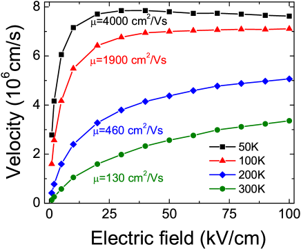
Utilizing the scattering rates, the velocity vs. field relation is obtained by a full-band Monte Carlo simulation at four different temperatures. As shown in Fig. 10, the extracted mobility decreases from cm2/Vs at 50 K to about cm2/Vs at room temperature while the saturation velocity changes from cm/s to cm/s. The small mobility and saturation velocity can be attributed to strong electron-phonon scattering as well as the heavy effective masses. With massive electrons that hinder acceleration and many states to scatter into (e.g., K, K′, Q, Q′ valleys), this is an expected outcome.
Compared to a recent theoretical estimation Kaasbjerg2012 of 410 cm2/Vs and experimentally extracted values Lembke2012 as high as 1090 cm2/Vs, however, our mobility is significantly smaller, requiring a careful analysis of the discrepancy. Two factors are identified that could yield at least a partial explanation. First, let us examine the issues surrounding the Q-K separation. With inconsistencies reported in several first-principles results on this sensitive quantity (see the discussion above), it is not unreasonable to imagine that our DFT calculation may have also experienced similar inaccuracies. If proves to be substantially larger than the estimated 70 meV, then the Q valleys would have a limited influence on the low-field mobility and can be neglected in the calculation as in Ref. Kaasbjerg2012, (with 200 meV). In this case, our simulation estimates the K-valley dominated mobility of 320 cm2/Vs that is essentially in agreement with the earlier prediction (410 cm2/Vs). Kaasbjerg2012 Clearly, both first-principles models produce a consistent picture of K-valley electron dynamics including intrinsic scattering with relevant phonon modes. The difference is the relative significance of Q valleys (e.g., 70 meV vs. 200 meV). As such, further clarification of intrinsic mobility in monolayer MoS2 may need to be preceded by accurate experimental determination of .
Even when the influence of Q valleys becomes negligible, a sizable disparity remains between the theoretically obtained mobility and the highest value claimed experimentally Lembke2012 (e.g., 320410 cm2/Vs vs. 1090 cm2/Vs). This is puzzling since the theoretical estimates of the intrinsic parameters are generally expected to provide an upper limit to the measured data that tend to experience additional mobility degrading, due to external scattering sources. When examining Ref. Lembke2012, , however, it becomes clear that the extracted data is not a direct measurement of intrinsic mobility; rather, it is the channel mobility that is strongly influenced by the details of the structure and the bias conditions. A particularly salient point is that the deduction relied on the transistor I-V data measured when the MoS2 channel is populated by electrons (i.e., degenerate). This condition deviates from the underlying assumption of nondegeneracy in our calculation, necessitating consideration of, among others, the screening effect. In a low-dimensional system, it is known that the screening due to the degenerate electrons can lower the bare scattering rates substantially (thus, affecting the mobility), Kawamura1992 ; Tanatar1993 as previously demonstrated experimentally in the AlGaAs/GaAs structures. Henriksen2005 The screening effect can be included by renormalizing the electron-phonon interaction through the dielectric function; i.e., . Kawamura1992 ; Tanatar1993
To gauge the potential significance in monolayer MoS2, we adopt a simple model for the dielectric function based on Thomas-Fermi screening of only the K-valley electrons: i.e., , where the screening wavevector . Here, the factor of accounts for the spin and valley degeneracies, is the electron charge, and is the background dielectric constant. Subsequent calculation with a rough estimate of shows that the scattering rates can experience a decrease of about an order of magnitude through screening. A corresponding increase of the mobility is estimated to be well over 1000 cm2/Vs that is more consistent with the value extracted from the transistor I-V characteristics. Lembke2012 Thus, it is evident that the screening must be taken into account accurately when the carrier density becomes degenerate in MoS2. A detailed analysis of is, however, beyond the scope of this investigation as our focus is on the properties of intrinsic electron-phonon interaction.
III.3 Deformation Potential Model
For practical applications, it would be convenient to approximate the ab initio results for electron-phonon coupling by a simple analytical model. Particularly useful in the present case is the deformation potential approximation. Under this treatment, the coupling matrix in Eq. (1) can be expressed in the first order (), or in the zeroth order (). Ferry2000 The first-order deformation potential constant () is adopted to represent the coupling matrices for the acoustic phonon modes in the long wavelength limit (i.e., intravalley scattering). In comparison, those involving the near zone-edge acoustic phonons (i.e., intervalley scattering) are treated by using the zeroth-order deformation potential () in a manner analogous to the optical modes. In the latter case (), the phonon energy is assumed independent of the momentum for simplicity. The obtained analytical expressions of the scattering rates are then matched to the first-principles results by fitting the effective deformation potential constants.
For silicene, the intravalley scattering rate by acoustic mode (= LA, TA, ZA) is obtained as
| (3) |
Here is the mass density ( g/cm2) and denotes the sound velocity, for which we can take the value of cm/s, cm/s, and cm/s, respectively, as discussed earlier. On the other hand, the rate of optical phonon scattering (both intravalley and intervalley transitions) as well as the intervalley acoustic phonon scattering can be expressed by the following form:
| (4) |
where (x) is the Heavyside step function and for phonon mode . Since the phonon dispersion is treated constant in Eq. (4), the intravalley optical phonon scattering approximates the zone-center (i.e., ) phonon energies for ( LO, TO, ZO). In the case of intervalley scattering via acoustic or optical phonons, takes the respective phonon energy at the zone-edge K point corresponding to electron transition . The specific values used in the calculation can be found in Table LABEL:table_ph_Silicene. When matched to the first-principles rates, the effective deformation potential constants can be extracted for each scattering process as summarized in Table LABEL:table_Silicene. A particularly interesting point to note from the result is that all three acoustic phonons show generally comparable values of and despite the large scattering rate of ZA mode (see also Fig. 3). Clearly, this mode (ZA) couples strongly with electrons but not enough to prevail over other acoustic branches; its dominant contribution is due mainly to the small phonon energy as discussed earlier.
The electron-phonon scattering processes in MoS2 are much more complicated as the deformation potentials need to be determined for both K- and Q-valley electrons. While feasible, it is not practically useful to define the effective interaction constants individually based on the mode of involved phonons and the transition types. Accordingly, we adopt a simplified description by combining the appropriate contributions into just two modes, acoustic and optical, respectively.
Using the effective mass approximation for the band structure near the valley minima, the scattering rate for intravalley acoustic phonon scattering (i.e., or by both LA and TA phonons; see Figs. 6 and 7) is given by
| (5) |
where g/cm2 for MoS2 and is the density-of-states effective mass for the K or Q valley (final state), ( K,Q). For electrons in the Q valleys, strictly speaking, an additional factor of is multiplied to the left side of Eq. (5) to account for the non-zero energy at the bottom of the Q valley. By taking the sound velocity ( cm/s), the value of is estimated to be 4.5 eV and 2.8 eV in the K and Q valleys, respectively.
The analytical expression that describes intravalley and intervalley optical phonon scattering as well as intervalley acoustic phonon scattering rate is obtained as
| (6) |
where is the valley degeneracy for the final electron states, and and denote the onset of scattering for phonon absorption and emission, respectively. For instance, and for electron transitions between the K valleys, whereas and for transitions between the Q valleys. The factors corresponding to intervalley transfer between K and Q valleys can be constructed accordingly, where may be treated as a potentially adjustable parameter. Tables LABEL:table_MoS2_K and LABEL:table_MoS2_Q summarize the initial/final electron states, the phonon momentum that is involved (in the form of its location in the momentum space), and the extracted deformation potential constants for each transition process considered in the investigation. For a given phonon momentum, the actual value used in the analytical calculation is the average of the relevant phonon modes. Specifically, the acoustic (optical) phonon energy is obtained as the average of LA and TA [TO(E′), LO(E′), and A1] modes at the respective symmetry points given in Table LABEL:table_ph_MoS2. An additional point to note is that the estimate of at the point includes the effect of Fröhlich scattering by the LO(E′) mode. Kaasbjerg2012 While this is a mechanism physically distinct from the deformation potential interaction and must be handled separately, its impact is relatively modest, at least for the electrons in the K valley. Accordingly, the present treatment is considered adequate. Further simplification of the model may also be possible judging from the narrow range of values in and (mostly in the low to mid 108 eV/cm).
IV Summary
We have performed a first-principles calculation together with a full-band Monte Carlo analysis to examine electron-phonon interaction and the intrinsic transport properties in monolayer silicene and MoS2. The results clearly elucidate the role of different branches as well as the intra/inter-valley scattering. The predicted intrinsic mobility for silicene is approximately 1200 cm2/Vs, with saturation velocity of cm/s at room temperature. In the case of MoS2, the K-valley dominated mobility gives approximately 320 cm2/Vs, while the intrinsic value reduces to about 130 cm2/Vs when the energy separation of 70 meV is used between the K and Q minima. The estimated saturation velocity is cm/s. The investigation also illustrates the significance of extrinsic screening, particularly in numerical evaluation of transport characteristics. The extracted deformation potential constants may prove to be useful in further studies of these materials.
Acknowledgements.
This work was supported, in part, by SRC/FCRP FAME, SRC/NRI SWAN as well as SRC CEMPI at the University of North Texas (Task ID P14924). MBN also wishes to acknowledge partial support from the Office of Basic Energy Sciences, US DOE at Oak Ridge National Lab under contract DE-AC05-00OR22725 with UT-Battelle, LLC. Calculations have been run at NCCS-ORNL and the NCSU-HPC Initiative.References
- (1) K. S. Novoselov, D. Jiang, F. Schedin, T. J. Booth, V. V. Khotkevich, S. V. Morozov, and A. K. Geim, Proc. Natl. Acad. Sci. 102, 10451 (2005).
- (2) J. N. Coleman, M. Lotya, A. O’Neill, S. D. Bergin, P. J. King, U. Khan, K. Young, A. Gaucher, S. De, R. J. Smith, I. V. Shvets, S. K. Arora, G. Stanton, H.-Y. Kim, K. Lee, G. T. Kim, G. S. Duesberg, T. Hallam, J. J. Boland, J. J. Wang, J. F. Donegan, J. C. Grunlan, G. Moriarty, A. Shmeliov, R. J. Nicholls, J. M. Perkins, E. M. Grieveson, K. Theuwissen, D. W. McComb, P. D. Nellist, and V. Nicolosi, Science 331, 568 (2011).
- (3) Q. H. Wang, K. Kalantar-Zadeh, A. Kis, J. N. Coleman, and M. S. Strano, Nat. Nanotechnol. 7, 699 (2012).
- (4) H. Şahin, S. Cahangirov, M. Topsakal, E. Bekaroglu, E. Aktürk, R. T. Senger, and S. Ciraci, Phys. Rev. B 80, 155453 (2009).
- (5) S. Cahangirov, M. Topsakal, E. Aktürk, H. Şahin, and S. Ciraci, Phys. Rev. Lett. 102, 236804 (2009).
- (6) A. Kara, H. Enriquez, A. P. Seitsonen, L. C. Lew Yan Voon, S. Vizzini, B. Aufray, and H. Oughaddou, Surf. Sci. Rep. 67, 1 (2012).
- (7) P. Vogt, P. D. Padova, C. Quaresima, J. Avila, E. Frantzeskakis, M. C. Asensio, A. Resta, B. Ealet, and G. L. Lay, Phys. Rev. Lett. 108, 155501 (2012).
- (8) K. F. Mak, C. Lee, J. Hone, J. Shan, and T. F. Heinz, Phys. Rev. Lett. 105, 136805 (2010).
- (9) S. Kim, A. Konar, W. S. Hwang, J. H. Lee, J. Lee, J. Yang, C. Jung, H. Kim, J. B. Yoo, J. Y. Choi, Y. W. Jin, S. Y. Lee, D. Jena, W. Choi, and K. Kim, Nat. Commun. 3, 1011 (2012).
- (10) B. D. Kong, C. Zeng, D. K. Gaskill, K. L. Wang, and K. W. Kim, Appl. Phys. Lett. 101, 263112 (2012).
- (11) B. Radisavljevic, A. Radenovic, J. Brivio, V. Giacometti, and A. Kis, Nat. Nanotechnol. 6, 147 (2011).
- (12) B. Feng, Z. Ding, S. Meng, Y. Yao, X. He, P. Cheng, L. Chen, and K. Wu, Nano. Lett. 12, 3507 (2012).
- (13) A. Fleurence, R. Friedlein, T. Ozaki, H. Kawai, Y. Wang, and Y. Yamada-Takamura, Phys. Rev. Lett. 108, 245501 (2012).
- (14) L. Chen, C. C. Liu, B. Feng, X. He, P. Cheng, Z. Ding, S. Meng, Y. Yao, and K. Wu, Phys. Rev. Lett. 109, 056804 (2012).
- (15) D. Lembke and A. Kis, ACS Nano 6, 10070 (2012).
- (16) D. Xiao, G. B. Liu, W. Feng, X. Xu, and W. Yao, Phys. Rev. Lett. 108, 196802 (2012).
- (17) T. Cao, G. Wang, W. Han, H. Ye, C. Zhu, J. Shi, Q. Niu, P. Tan, E. Wang, B. Liu, and J. Feng, Nat. Commun. 3, 887 (2012).
- (18) H. Zeng, J. Dai, W. Yao, D. Xiao, and X. Cui, Nat. Nanotechnol. 7, 490 (2012).
- (19) K. F. Mak, K. He, J. Shan, and T. F. Heinz, Nat. Nanotechnol. 7, 494 (2012).
- (20) K. Kaasbjerg, K. S. Thygesen, and K. W. Jacobsen, Phys. Rev. B 85, 115317 (2012).
- (21) S. Baroni, S. de Gironcoli, A. Dal Corso, and P. Giannozzi, Rev. Mod. Phys. 73, 515 (2001).
- (22) K. M. Borysenko, J. T. Mullen, E. A. Barry, S. Paul, Y. G. Semenov, J. M. Zavada, M. Buongiorno Nardelli, and K. W. Kim, Phys. Rev. B 81, 121412(R) (2010).
- (23) P. Giannozzi, S. Baroni, N. Bonini, M. Calandra, R. Car, C. Cavazzoni, D. Ceresoli, G. L Chiarotti, M. Cococcioni, I. Dabo, A. Dal Corso, S. de Gironcoli, S. Fabris, G. Fratesi, R. Gebauer, U. Gerstmann, C. Gougoussis, A. Kokalj, M. Lazzeri, L. Martin-Samos, N. Marzari, F. Mauri, R. Mazzarello, S. Paolini, A. Pasquarello, L. Paulatto, C. Sbraccia, S. Scandolo, G. Sclauzero, A. P. Seitsonen, A. Smogunov, P. Umari, and R. M. Wentzcovitch, J. Phys.: Condens. Matter 21, 395502 (2009).
- (24) Y. C. Cheng, Z. Y. Zhu, and U. Schwingenschlögl, Eur. Phys. Lett. 95, 17005 (2011).
- (25) N. D. Drummond, V. Zólyomi, and V. I. Fal’ko, Phys. Rev. B 85, 075423 (2012).
- (26) S. Piscanec, M. Lazzeri, F. Mauri, A. C. Ferrari, and J. Robertson, Phys. Rev. Lett. 93, 185503 (2004).
- (27) J. L. Mañes, Phys. Rev. B 76, 045430 (2007).
- (28) X. Li, B. D. Kong, J. M. Zavada, and K. W. Kim, Appl. Phys. Lett. 99, 233114 (2011).
- (29) W. Cai, A. L. Moore, Y. Zhu, X. Li, S. Chen, L. Shi, and R. S. Ruoff, Nano Lett. 10, 1645 (2010).
- (30) A. Molina-Sánchez and L. Wirtz, Phys. Rev. B 84, 155413 (2011).
- (31) E. S. Kadantsev and P. Hawrylak, Solid State Commun. 152, 909 (2012).
- (32) N. Wakabayashi, H. G. Smith, and R. M. Nicklow, Phys. Rev. B 12, 659 (1975).
- (33) C. Lee, H. Yan, L. E. Brus, T. F. Heinz, J. Hone, and S. Ryu, ACS Nano 4, 2695 (2010).
- (34) T. Kawamura and S. Das Sarma, Phys. Rev. B 45, 3612 (1992).
- (35) B. Tanatar, Phys. Rev. B 48, 12001 (1993).
- (36) E. A. Henriksen, S. Syed, Y. Ahmadian, M. J. Manfra, K. W. Baldwin, A. M. Sergent, R. J. Molnar, and H. L. Stormer, Appl. Phys. Lett. 86, 252108 (2005).
- (37) D. K. Ferry, Semiconductor Transport (Taylor and Francis, New York, 2000).
| Phonon modes | |||
|---|---|---|---|
| ZA | 0 | 13.2 | 13.0 |
| TA | 0 | 23.7 | 13.4 |
| LA | 0 | 13.2 | 13.5 |
| ZO | 22.7 | 50.6 | 50.7 |
| TO | 68.8 | 50.6 | 56.7 |
| LO | 68.8 | 61.7 | 64.4 |
| Phonon modes | ||||
|---|---|---|---|---|
| TA | 0 | 23.1 | 19.2 | 17.9 |
| LA | 0 | 29.1 | 29.2 | 23.6 |
| TO(E′) | 48.6 | 46.4 | 48.2 | 48.0 |
| LO(E′) | 48.9 | 42.2 | 44.3 | 44.2 |
| A1 | 50.9 | 51.9 | 50.1 | 52.2 |
| Phonon mode | Intravalley | Intervalley |
|---|---|---|
| ZA | 2.0 eV | 6.1107 eV/cm |
| TA | 8.7 eV | 1.4108 eV/cm |
| LA | 3.2 eV | 4.2107 eV/cm |
| ZO | 6.3107 eV/cm | 4.3107 eV/cm |
| TO | 1.8108 eV/cm | 1.4108 eV/cm |
| LO | 1.9108 eV/cm | 1.7108 eV/cm |
| Phonon | Electron | Deformation |
| Momentum | Transition | potentials |
| =4.5 eV | ||
| = eV/cm | ||
| = eV/cm | ||
| = eV/cm | ||
| = eV/cm | ||
| = eV/cm | ||
| = eV/cm | ||
| = eV/cm |
| Phonon | Electron | Deformation |
| Momentum | Transition | potentials |
| =2.8 eV | ||
| = eV/cm | ||
| = eV/cm | ||
| = eV/cm | ||
| = eV/cm | ||
| = eV/cm | ||
| = eV/cm | ||
| = eV/cm | ||
| = eV/cm | ||
| = eV/cm | ||
| = eV/cm | ||
| = eV/cm |

