Electron optics with dirac fermions: electron transport in monolayer and bilayer graphene through magnetic barrier and their superlattices
Abstract
In this review article we discuss the recent progress in studying ballistic transport for charge carriers in graphene through highly inhomogenous magnetic field known as magnetic barrier in combination with gate voltage induced electrostatic potential. Starting with cases for a single or double magnetic barrier we also review the progress in understanding electron transport through the superlattices created out of such electromagnetic potential barriers and discuss the possibility of experimental realization of such systems. The emphasis is particularly on the analogy of such transport with propagation of light wave through medium with alternating dielectric constant. In that direction we discuss electron analogue of optical phenomena like fabry perot resonances, negative refraction, Goos-Hänchen effect, beam collimation in such systems and explain how such analogy is going to be useful for device generation. The resulting modification of band structure of dirac fermions, the emergence of additional dirac points was also discussed accompanied by brief section on the interconvertibility of electric and magnetic field for relativistic dirac fermions. We also discuss the effect of such electromagnetic potential barrier on bilayer graphene in a similar framework.
pacs:
81.05. Ue, 73.63.-b, 78.20.Ci, 42.25.Gy, 73.43.QtI Introduction
Physically Maxwell’s equation that describes the propagation of electromagnetic wave/light through free space and dielectric medium, namely
| (1) |
and Schrdinger equation that describes the time evolution of probability amplitude or de Broglie wave in quantum systems, namely
| (2) |
correspond to the different type of phenomena. However, their striking mathematical similarity indicates that a large number of wave like phenomena will occur in either of these cases. Whereas the motion of a isolated single electron in presence of potential barrier is described by the wave Eq.(2), in real materials due to the scattering by other electrons, impurities etc. the motion of the charge carriers is generally diffusive. Therefore, such wave propagation based description of the electron transport becomes only meaningful if the electron mean free path is of the order the typical sample size. Such a transport regime is called the ballistic transport regime and in that regime the similarity between the propagations of transport electrons and electromagnetic wave or light promises rich dividend dutta ; analogy .
A particular consequence of the similarity between the wave equations (1) and (2) is that for a monochromatic wave with a given frequency in Eq. 1 the role played by the dielectric constant of a given medium has its corresponding analogue in the the potential landscape for a stationary solution of the Schrdinger electron described by Eq. 2. Thus some of the effects that one obtains by spatially modulating the potential in a Schrdinger equation can be reproduced for the light also by spatially modulating the dielectric constant of the medium. Indeed this was pointed out in seventies in the pioneering work by Yariv and collaborators yariv that the propagation of light through a medium with periodically modulated dielectric constant will lead to the similar band structure of transport electron as observed in Kronig-Penny model Kittel . In this context it is particularly useful to point out that for conventional two dimensional electron gas (2DEG), the analogy between transmission of de Broglie waves satisfying the Schrdinger equation through a one-dimensional electrostatic potential SIVAN90 ; Stormer and light propagation in linear dilelectric medium is well established and led to the development of a number of applications.
The recent discovery of graphene Wallace ; KSN1 ; KSN2 ; YZ1 added a new twist to this well established optical analogy of ballistic electron transport and vice versa. In graphene, electrons near the Fermi level, namely the transport electrons no more obeys quadratic dispersion law, a typical characteristics of their non-relativistic nature, but rather obeys a linear dispersion relation at or near the Fermi surface, an archetypical of the ultra relativistic massless particles. Hence they are called massless Dirac fermions. It has now been established that transport of such massless Dirac fermions in the presence of an electrostatic potential barrier is analogous to negative refraction through metamaterials cheinov ; Veselago ; pend85 . The relativistic behaviour of graphene electrons also leads to Klein tunnelling KSN3 , where a massless relativistic particle can tunnel through any potential barrier above the Fermi surface, invalidating the possibility of confining it using such potential barriers.
In the context of electronic transport in graphene devices that are proposed for graphene based electronic in future, the local carrier concentration is controlled by one or more local gates. Particularly, in the cleanest devices which satisfy the criterion of ballistic transport, transport signatures of the relativistic nature of the charge carriers of graphene are observed. A vast body of theoretical work ( for a review see Youngreview ) has already been devoted to the study of multigated graphene superlattices which can form a basis for a new kind of electronic optics based on graphene as an electronic metamaterial. However the inability of confining the electrons using a electrostatic potential barrier severely limits the applicability of such devices. A solution to that problem was proposed by De Martino et al. eggerprl when it was pointed out that well localized magnetic field dubbed as magnetic barrier can confine massless dirac fermions in graphene. This suggests that one way of making high mobility graphene based electronic devices is to make locally gated structures in conjunction with such magnetic barriers. Given this context it is extremely important to see what will happen to the above mentioned optical analogy when it applies to the cases of such magnetic barriers.
However it may be pointed out that the study of transport properties of two dimensional non relativistic electron system in the presence of a transverse magnetic field remains mostly confined to the case where the magnetic field is uniform on the scale of sample size through phenomena such as Integer and Fractional Quantum Hall effect. Study of electron transport in inhomogenous magnetic field is relatively lesser known field nogaretjpcm , even though inhomogenous magnetic field is being used for many other purpose for a long time, such as one in the famous Stern Gerlach experiment sterngerlach . In a homogenous magnetic field, the electrons execute cyclotron motion, the direction of the wavevector continuously changes, hence rendering any analogy with the monochromatic light propagation in dielectric medium is very unlikely. In quantum mechanical language the electronic wavefunction is localized over the scale of the magnetic length. Thus a direct analogy with a propagating wave is not possible.
This situation however changed, when it was pointed out sgms that an optical analogy can be constructed for electron transport in graphene in presence of highly inhomogenous magnetic field peetersprl where one does not get bound state solutions, but rather scattering state solutions. This suggests that inhomogenous magnetic field not only confine massless dirac fermions eggerprl , but the ballistic transport through such barriers can also be understood in terms of suitable optical analogy. Ref. sgms also showed that the analogy with light propagation in medium with periodically modulated dielectric constant can again be constructed by considering the transport of massless dirac fermions in graphene through the periodic arrangement of such highly inhomogenous magnetic field. Subsequent work mssg showed that a very rich transport regime can be realized for such graphene electrons by considering structures where a local gate voltage is used simultaneously with such magnetic barrier. When such configurations are generalized to a superlattice structure, that significantly modifies the band structure of graphene electrons. Subsequently a large volume of theoretical work pointed out the relevance of such optical analogy and proposed device structures based on that. Other properties such as Goos Hänchen shift of graphene electrons by these type of barriers, collimation of the electron beam, generation of additional Dirac points was also discussed in further works. It was also extended in the case of bilayer graphene. In the current review article we plan to review these developments. The purpose is two fold. One, is to review the general theoretical framework in a pedagogical way, highlighting a number of significant work done in this subfield of graphene research. The other purpose is to indicate in very clear terms the possibility of designing interesting experiment and novel device structure that holds rich promises for graphene based electronics.
The organization of the article is as follows. After giving a brief review of low energy description of charge carriers in graphene, first we explain how electron transport through scalar electrostatic barriers and magnetic barriers is explained in the language of geometrical optics. Next, we explain how such transport gets modified when various types of potential barriers are created atop magnetic barriers. We discuss Goos-Hänchen shift and fabry perot resonances in this type of structure. Then we provide an analysis of transport through an infinite series of such barriers pointing towards an effective way of changing the bandstructure. Here we also discuss the collimation of the electron beam, emergence of extra dirac point etc. We then briefly discuss the issue of interconvertibilty of electrostatic potential and vector potential due to magnetic field citing relativistic invariance of the equation obeyed by transport electrons in graphene. Then we come to the issue of electron transport through graphene bilayer in presence of such potential barriers. The dispersion relation for graphene bilayer is very different from that of monolayer graphene. The charge carriers in bilayer graphene have a parabolic energy spectrum, which means they are massive, similar to conventional non relativistic electrons. On the other hand, due to the crystal structure of graphene consisting of two sublattices, these particles are described by spinor wave functions similar to that of monolayer graphene. We study how the transport of such electrons in graphene bilayer is affected, again when exposed to combination of magnetic barriers and voltages.
I.1 Low energy description of charge carriers in graphene
The interesting band structure of graphene was pointed out by Phil Wallace Wallace way back in 1947. After its experimental discovery by Geim, Novoselov, Kim and their collaborators there are many excellent review articles (for example see Castroneto ) where the band structure, the resulting dirac fermion nature of the charge carriers are detailed. Here we provide a brief introduction to the low energy description of these charge carriers for completeness. Graphene is a one atom thick planar sheet of bonded carbon atoms. The carbon atoms are distributed at the edges of regular hexagons forming a honeycomb lattice. However, the honeycomb lattice is not a Bravais lattice and, from a crystallographic point of view, has to be described by two inter penetrating triangular lattices with two atoms (sublattice A and B) per unit cell.
Each carbon atom has four valence electrons, three of which hybridize to form hybridized orbitals to form sigma bonds with neighbouring atoms. However, the fourth unbound electron lies in the orbital which extends vertically above and below the plane. It is this electron which interacts with the periodic field of the hexagonal crystal lattice of graphene. If we denote the creation operator by for an atom on the A(B) sublattice, then the nearest neighbour tightbinding Hamiltonian has the simple form pereirarev ; fuchs
| (3) |
where is the nearest neighbour hopping parameter. The tightbinding eigen functions has the form of bispinor, whose components corresponds to the amplitudes on sublattice A and B respectively within the unit cell. This also means that in addition to its usual spin , electrons carriers an additional pseudo-spin associated with its sublattice degree of freedom. The energy levels of the lattice can be determined by operating with the Hamiltonian on its eigen function to give the corresponding band structure:
| (4) |
where with lattice parameter, .
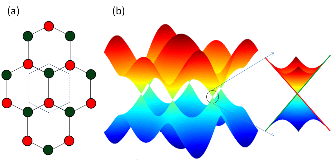
In Eq.(4) the plus sign refers to the upper () band and the minus sign refers to the lower () band. The unique feature of the band structure of graphene saito ; dressdress is that its valence band and conduction band touch each other at 6 specific points, which are also the vertices of the hexagonal Brillouin zone of this honeycomb lattice ( see Fig. 1). Out of these six points, only two and are non-equivalent and all the rest are related to these two points by symmetry. These points are also known as the points in the literature and their positions in the reciprocal space are:
Under ambient conditions, also known in the literature as zero biased doping, the Fermi level coincide with these corners of the hexagonal Brillouin zone. Thus, to understand the low energy charge transport properties of graphene one expands the full band structure close to the point by writing , with and then by keeping the first order term and neglecting all higher order terms in , the resulting dispersion relation is of the form such that low energy quasiparticles of graphene are described by the Dirac-like Hamiltonian szwski ; semenoff ; haldane
| (5) |
where is the fermi velocity, is the vector comprising of two component Pauli matrices, and is momentum vector in plane. Thus, charge carriers in graphene behave like massless relativistic fermions dubbed as massless Dirac fermions with only the velocity of light is replaced by the Fermi velocity. This way, the behaviour of transport electrons in graphene is very different from those in ordinary semiconductors where they have a parabolic dispersion like a non-relativistic free particle. In the following sections we shall describe how such charge carriers with ultra relativistic dispersion laws transports in presence of highly inhomogenous magnetic field dubbed as magnetic barriers in combination with local gate voltages.
II Electron transport in graphene : Optical analogy
II.1 Electron optics in the presence of scalar potential barriers
In a two dimensional electron gas (2DEG) it is well-established that transmission of de Broglie waves satisfying the Schrdinger equation through a one-dimensional electrostatic potential is similar to light propagation through a refractive medium. Such transport can be understood in terms of phenomena like reflection, refraction and transmission, leading to an analogy between electron transport and light propagation SIVAN90 ; Stormer ; dutta . When a non-relativistic electron in a 2DEG with quadratic dispersion, at Fermi energy , is incident on a potential barrier , its momentum parallel to the interface outside and inside the barrier is conserved; i.e., , where are the momenta and are the angles they make with surface normals respectively in the regions without and with potential barrier. This leads to the following Snell’s law:
| (6) |
Graphene charge carriers however do not have the quadratic dispersion, but instead behave as massless Dirac-Weyl fermions leading to a different set of transport phenomena KSN1 ; KSN2 ; YZ1 ; Geimreview ; Castroneto ; Beenakker . The optical analogues of such electron transport can again be constructed by considering the charge carriers in MLG incident on an electrostatic potential barrier . Such charge carriers in monolayer graphene (MLG) obey the following Dirac-Weyl like equation:
| (7) |
where in the barrier region () and vanishes outside, and is the two component wavefunction with denoting the transpose of the row vector. We assume to be the one dimensional potential. Due to the y invariance of potential barrier we consider the solutions of the form . On substituting this in Eq.(7), two coupled equations in and are obtained as:
The above two off-diagonal equations can be decoupled in terms of to give a Schrdinger like equation of the form
| (8) |
which admits exponential solutions,namely .
By parameterizing the energy momentum relation in polar coordinates, we obtain
The momentum component along a straight interface should be conserved. Accordingly, using the electron momentum conservation in the y direction at the left interface , we obtain the Snell’s law in the following form:
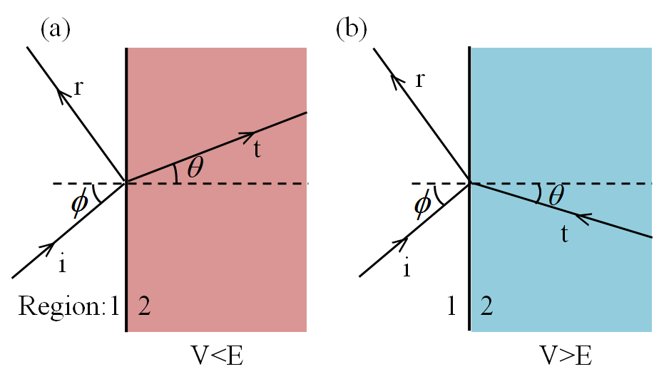
Clearly for , the barrier acts like a medium with negative refractive index cheinov . This is shown in Fig.2
| (9) |
This corresponds to the electronic analogue of the well known phenomenon of negative refraction, which occurs in left handed metamaterials and which was first proposed by Veselago Veselago and subsequently developed in more detail by Pendri and collaborators pend85 . If one uses so called split gate voltage by placing the region and side by side ( Fig. 2), the Fermi level can be tuned below and above the Dirac point. Since the region below and above the charge neutral Dirac points are respectively hole and electron states for such Dirac fermions, this creates and type region in graphene simply by changing the height of of the electrostatic potential barrier in a given region cheinov . The resulting structure is called graphene junction. Consequently, a graphene junction can be used as a Veselago lense for electron focussing. Similarly circular graphene p-n junctions has also been studied showing the formation of caustics jozsef .
II.2 Klein Tunneling
While electrostatic potential barriers can indeed manipulate charge transport in graphene, an electron could tunnel through any high barrier in contrast to the conventional tunnelling of non-relativistic electrons ando ; KSN3 . This behaviour, called Klein tunnelling in graphene, leads to several observable transport effects related to transport some of which have been demonstrated in graphene kleinexp ; kleinexp1 and also in carbon nanotubes Steele . Below we review briefly the work on such tunnelling problem for graphene charge carriers in the presence of an electrostatic potential barrier. This analysis will then be extended to similar transport through inhomogenous magnetic fields and will be followed by comparing and contrasting these transport to electrostatic and magnetic barriers, which is the central topic of this review article.
The wavefunction solutions in the presence of a potential barrier can be obtained by solving Eq.8. These solutions in any region of space can be written in terms of linear combination of forward and backward propagating plane waves such that
| (10) |
where is the Fermi wavevector, and are the wavevector components outside the barrier, , is the refraction angle, and .
By taking into account the continuity of wave-function components and at the boundaries of the barrier the transmission and reflection coefficients are obtained as
| (11) | |||||
| (12) |
Here is the width of the barrier. Clearly corresponds to the resonance condition at which the barrier transmission is unity. This corresponds to usual resonant tunnelling through a potential barrier and occurs for non relativistic electron as well. However remarkably, the above expression also shows that barrier always remains transparent for normally incident carriers, ie. when . This feature of anomalous tunnelling in graphene is peculiar to the Dirac like spectrum for graphene charge carriers and is explained as follows: As explained briefly in section I.1, the gapless, conical spectrum of graphene is the result of intersection of two cosine like energy bands originating form sublattices A and B. (represented in green and red for A and B sublattice respectively, see fig.1). Due to this, the sublattice degree of freedom i.e. pseudospin should remain fixed on each branch. This also means that an electron with energy and possessing wavevector will originate from the same branch as a hole with energy and possessing wavevector . Above two features allows the introduction of chirality for graphene charge carriers. The term present in the Hamiltonian (5) gives the chirality, namely projection of pseudospin on the direction of motion,
and has two possible eigen values, (for electrons) and (for holes). This operator is same as the usual helicity operator for -dimensional relativistic electrons that obey Dirac equation Greiner , but redefined for charge carriers in graphene which obeys dimensional Dirac-Weyl equation. In the absence of any potential, the chirality operator commutes with the Hamiltonian and is therefore a conserved quantity. For normally incident carriers, the chirality remains conserved even in the presence of an external electrostatic potential . This can be shown as follows: For normally incident carriers,
Hence
Also the velocity operator
Thus the velocity operator is same as the chirality which is a conserved quantity for this case fuchs ; todorovskiy . The velocity along the direction is therefore a constant of motion and thus cannot be reversed. This leads to perfect transmission through such a barrier at normal incidence. This is what describes Klein tunnelling in MLG KSN3 . This is to be noted here that a rectangular electrostatic barrier in graphene assumes that the gate voltage-induced doping changes abruptly at the edges . In reality, however, the doping level continuously changes and thus the edge of the potential barrier is actually smooth and not sharp. This issue has been considered for scalar potential barrier in Ref.falko , where it was found that a potential which is smooth on the scale of the Fermi wave length for small angles of incidence, where is the barrier width. A comparison with the transmission expression given in Eq.11 shows that the assumption of the rectangular barrier captures the effect of Klein tunnelling correctly. However, at other angles close to the normal incidence it overestimates the transmission. Transmission through trapezoidal barrier was also analysed in Ref.Sonin which combines the effect of a smooth barrier and a rectangular barrier.
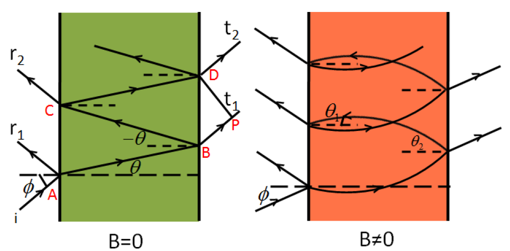
On expanding in eq.(12), close to the normal incidence, namely , by substituting , it can be seen that the reflection amplitude r undergoes a phase jump when the incident angle goes from positive to negative value . At zero magnetic field, at non-normal incidences, the two consecutive reflections on the two p-n interfaces occur with opposite angles and (Fig.20). When such a system is placed in a transverse magnetic field , the electronic trajectories bend in the presence of magnetic field. And above a critical field value , trajectory bending becomes sufficient to make the two consecutive reflections occur with the same incident angle which is exactly the case what happens at normal incidence in the absence of magnetic field. This suddenly adds to the phase accumulated by an electron between two reflections and shifts the interference fringes by half a period shytov . The observation of this half-period shift in Fabry Perot interference fringes is therefore a direct evidence of perfect tunnelling at normal incidence kleinexp . We analyse this in more detail in section IV.4. An alternative way of demonstration of Klein tunnelling in graphene p-n junctions has been addressed in kleinexp1 . This was done by probing the transition from clean to disordered transport across a single steep p-n junction. Very recently, an angle dependent carrier transmission probability in graphene p-n junctions has also been investigated experimentally sutar and theoretically avik where it is shown that chiral tunnelling can be directly observed from the junction resistance of a tilted interface probed with separate split gates.
III Electron transport in the presence of inhomogenous magnetic field profile
While the above mentioned absence of backscattering by a scalar potential due to Klein tunnelling is a very interesting phenomenon, this implies that confining transport electrons in graphene by a potential barrier is not possible in a conventional way. This leads to problem in device making. For example, even though it is easy to make a junction in graphene, reverse biasing such junction will be very difficult for Klein tunnelling. For the designing of graphene based electronics it is crucial to attain confinement of electrons within a mesoscopic or nanoscopic size of the sample. For this reason, several alternatives have been suggested. One way is to exploit the fact that suitable transverse states in a graphene strip may allow one to circumvent Klein tunnelling silvestrov . Other schemes that have been proposed include gated nanoribbons trauzette , gated milton or doped pereira bilayer etc. Yet another possibility was demonstrated theoretically in eggerprl ,eggerssc by making use of external inhomogeneous magnetic fields applied perpendicular to the graphene plane. This brings us to the the main focus of this review article- to investigate the electron transport in the presence of inhomogenous magnetic field viz. magnetic barrier(s) in graphene. Before proceeding further we first discuss the experimental strategies for creating such inhomogenous magnetic fields and point out that such magnetic barriers are already in very much use in other materials.
III.1 Producing inhomogenous magnetic field profile: Experimental strategies
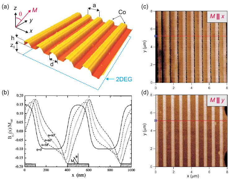
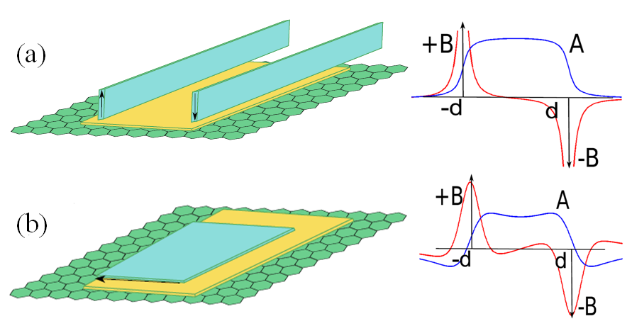
A microscopically inhomogenous magnetic field can be created for charge carriers in graphene by placing a graphene sheet in close proximity to long magnetic stripes that produce highly localized magnetic fields. Such field profiles can be generated using demagnetizing fields produced at the edges of narrow stripes made with hard ferromagnetic (FM) materials of either perpendicular or in-plane anisotropy. The magnetic field of such structures is given as
where for perpendicular magnetization, and for magnetization parallel to the graphene sheet. is a constant dependent on the aspect ratio of the stripe.
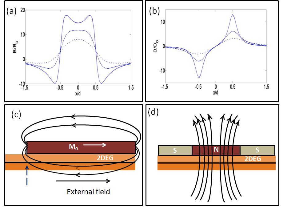
For a given value of we plot in Fig.3(a), (b) the profile of such a magnetic field. The major component of the demagnetizing field reaches the graphene monolayer and produces the desired field profile. Though there is always some component of the demagnetizing field that will give rise to undesired fringe fields in other directions, these can be substantially lowered by suitable magnetic design of the stripes. Such nanostructures are routinely used in magnetic recording media appphys . Materials such as CoCrPt produce fields of 1 Tesla close to the surface with bit lengths ranging from 50-100 nm. For example, in IEEE , isolated tracks of single-domain magnetic islands have been fabricated using focused ion-beam lithography for both perpendicular and parallel anisotropy using CoCrPt. Here, patterns with successive magnetizations pointed along opposite directions were achieved. In another recent work, off-axis electron holography has been used to probe the magnetization structure in high density recording medium by using perpendicular magnetic anisotropic (PMA) recording medium dipole . The direct imaging of magnetization done shows that the foils of PMA material consist of successively reversed highly stable domain structures of few ten’s of nanometer size. In practice, one can also change the strength of the magnetic field by suitable adjusting the width of such PMA material. Precise design of read-write structures for recording individual bits at these dimensions has also been achieved nphotonics . Using the above discussed techniques, typical magnetic barriers can be patterned down to 50-100 nm widths.
Apart from the above mentioned method of using ferromagnetic materials mancoff there are several other ways in which inhomogenous magnetic fields have been experimentally realised in conventional semiconductors. One such way is through the integration of superconducting elements, which may be used to screen the externally applied magnetic field in accordance with Meissner effect. When an external magnetic field is applied the flux lines will be expelled from the superconductor due to the Meissner effect. If the latter is close enough this will result in an inhomogeneous magnetic field in the 2DEG vonklitzing1 geimjetp . This is shown schematically in [Fig.3(d)]. As an example, in ref. vonklitzing1 , it was shown that with type II superconducting films deposited on top of the two-dimensional electron gas in a GaAs/AlGaAs heterostructure, the distribution at the 2DEG takes the form of flux tubes which are much narrower than an electron inelastic scattering length. The superconducting materials used in these experiments were typically 200nm of lead (Pb), 400 nm of a lead/indium [Pb(1 at. In)] alloy, and 200 nm of niobium nitride (NbN), as being materials whose characteristic superconducting length scales span a broad range. Growing the heterojunction on top of a pre-etched (nonplanar) substrate can also give rise to inhomogeneous magnetic fields leadbeater -grayson . When a uniform external field is applied on such a system, the angle between the field direction and the normal to the 2DEG depends on the tilt of the facet and therefore will have a normal component of magnetic field which varies spatially across the sample. Since it is only the normal component of magnetic field that influences the transport, by varying the facet length and angle, as well as the angle between the applied field and the normal to the substrate, a wide variety of field profiles can be generated.
In other studiesapl6 -kubrak a similar yet simpler approach was used based on the idea that if a thin magnetic film is placed on top of a heterostructure its in-plane magnetization can be saturated in an external in-plane magnetic field [Fig.3(c)]. In this case the out-of-plane component of the fringe field under the edge of the film creates a magnetic barrier for electron transport with a width of the order of 100 nm determined by the separation of the 2DEG from the magnetic film. Magnetic field strengths of more than 0.5 T have been realized in this way kubrak . A detailed discussion on experimental methods used for applying magnetic modulations to 2DEGs can be found in the review article nogaretjpcm .
III.2 Magnetic confinement of massless dirac fermions in graphene
In the previous section we reviewed the experimental progress of realizing inhomogenous magnetic field or magnetic barrier over a wide range of length scales in a number of systems. Mesoscopic transport in presence of inhomogenous magnetic fields has been studied theoretically soumaphyreports , peetersprb48 - ibrahimpeetersprb52 for non relativistic electrons . Related experimental studies also took place in conventional semiconductor heterostructures, e.g., transport in the presence of magnetic barriers johnson and superlattices carmona , magnetic edge states close to a magnetic step nogaret , and magnetically confined quantum dots or antidots dubonos . In the following section B we review the transport of massless Dirac fermions in graphene in the presence of of magnetic barriers with some suitable examples.
The magnetic barrier profile chosen here is in the form of step like function eggerprl ; eggerssc as
| (13) |
, and the vector potential chosen in Landau gauge in region , and respectively.
Typically, the equation of motion of charge carriers at the two inequivalent Dirac points K and are decoupled from each other shon in the absence of intervalley scattering which gives a wave vector change of the order of . We assume for the cases to be considered this condition is satisfied. Under this situation motion near each Dirac point can be treated separately. The stationary solutions near each such point is given by a two component spinor and satisfies the equation
| (14) |
Here, is the fermi velocity () and . Using as the unit of length scale such that and as the unit energy such that and in the Landau gauge, Eq.14 can be rewritten as
| (15) |
which can be decoupled to obtain the following Schrdinger like equation:
| (16) |
where sign in the above expression corresponds to region respectively.
Upon solving, we obtain the solutions outside the barrier as propagating solutions while inside the barrier the solutions are localised and can be written in terms of parabolic cylindrical functions gradshteyn .
| (17) |
| (18) |
where , , stands for parabolic cylindrical function, and and corresponds to the incidence and emergence angle in regioin I and III respectively.
The emergence angle can be obtained by conservation condition of as:
| (19) |
An alternative way of writing the above equation is
where and , is the net flux enclosed by an area . The second form particularly shows how the flux enclosed by the area containing the barrier changes the refractive index of this region in a non specular way.
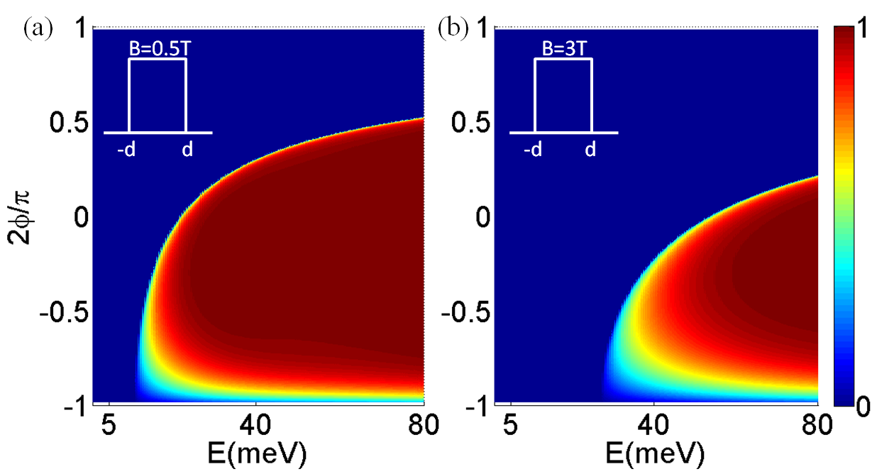
The transmission through such magnetic barrier can be obtained by matching the wavefunction at the boundaries of the barrier, , where the prefactor ensures the current conservation in the system. The transmission as function of incidence angle and incident energy is shown in fig.5. As one can see, Eq. 17 and 18 depicts the formation of localised states inside the barrier region. However these states are bound only in the direction perpendicular to the barrier but can propagate in the direction along the inhomogeneity of the magnetic field. The transmission, for this reason, depends very strongly on the incident wavevector and facilitates the possibility to construct wave-vector filter Masir1 . Fig. 5 depicts this situation clearly. The requirement of the propagating solutions in the incident region and region of exit determines the range beyond which no transmission is possible, thereby leading to the possibility of confinement. This is how magnetic barrier turn reflective for a set of wave vector for the massless Dirac fermions. In the following section we shall illustrate this property more clearly by building clear optical analogy of electron transmission through the extremely inhomogeneous magnetic barrier where the magnetic field profile can be approximated as a delta function.
IV Massless dirac fermions in inhomogenous magnetic fields: An analogy with light propagation
IV.1 Magnetic vector potential (MVP) barrier
The issue addressed here is whether the transport through such magnetic barrier can be understood in terms of propagation of light through medium with changing dilelectric constant using well known ideas in geometrical opticssgms . Even though such idea was developed for the ballistic electron transport through electrostatic potential barrier, generalizing this concept in presence of a magnetic field was non trivial since in the presence of magnetic field electron executes cylotron motion and the wave vector is not a good quantum number for such motion. Thus to yield a Snell’s law like one in Eq. (9) in presence of a magnetic barrier, it is essential that the electron should not complete its half cyclotron radius beyond which it get completely localised inside the barrier. This situation can be realized in the presence of a highly inhomogeneous magnetic field. Particularly, if the range of inhomogeneity is much smaller than the cyclotron radius, one is left with plane wave-like scattering states. Thus, such field profile scatter the electrons in the same way as an electrostatic potential does.
For this to be valid, two conditions must be satisfied. First, the magnetic length should be similar in order to the width of such magnetic barriers. Second, the de Broglie wavelength should be much larger than the barrier width so that the electron will not see the variation in the vector potential inside the barrier. An extreme case of such an inhomogeneous magnetic field is singular magnetic barrier - the one introduced in peetersprl ; ibrahimpeetersprb52 ; magb2 ; sgms ; mssg ; neetuinsa ; Masir1 , which gives rise to step-function like magnetic vector potential (MVP) barriers. Here, we shall consider the scattering of massless Dirac fermions by such singular magnetic barriers as in Eq.20. Such field profiles having highly localized field variations are well known in literature and have been realized experimentally as we have already pointed out in the section III.1. Patterned stripes down to length scales as low as 10 nm have been realized using nanolithography terriskrawczykbader . It is possible to achieve field profiles at even smaller dimensions using domain walls with widths in the range of 10-50nm and magnetic nanostructures down to 5 nm sunsci ; zhengFePt and 0.15 nm bergmann having highly localized field variations which can be approximated as such delta function barriers.
IV.1.1 Electron optics with MVP barrier
The most elementary of such magnetic field profile that satisfy the flux line closure condition and its vector potential in the Landau gauge can be given as :
| B | (20) | ||||
In the absence of intervalley scattering, the charge carriers in graphene in the presence of above potential form can be described by Eq.14 which can be rewritten in the form of the following coupled equation
| (21) |
Here for and for . The coupled equations Eq.21 can be decoupled easily and results in a Schrdinger like equation of the form
| (22) |
Thus, in the barrier region electrons see a momentum-dependent barrier of height . Hence such a barrier will be termed as magnetic vector potential barrier (MVP).
Since magnetic field doesn’t do any work, the energy conservation gives for and for . By parameterizing the above two equations in polar co-ordinates as shown in Fig. 7, we obtain the relation
| (23) |
The situation is depicted in Fig.7. For a wave incident with positive wave vector bends away from the normal whereas for a wave incident with negative incidence angle the corresponding wave vector bends towards the surface normal inside the barrier region. Here, is the angle of refraction (denoted as for positive and negative angles of incidence). Clearly, the Snell’s law for electron waves in such magnetic barriers is not specular as it is for light waves on smooth surfaces or for the incidence of the electrons on an electrostatic potential barrier cheinov , KSN3 .
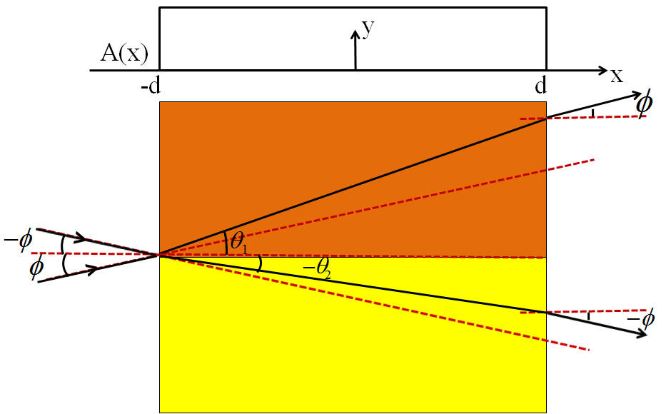
According to Eq.23, when , becomes imaginary and the wave in the second medium becomes evanescent. In the language of optics this corresponds to total internal reflection (TIR). According to Fig. 8, this will happen when for and when for . In the latter case, this requires the wave vector to be negatively refracted falko at sufficiently high magnetic field before TIR occurs. It also follows that for a given strength the magnitude of critical angle of incidence for TIR is higher for as compared to the one for . Because of TIR the transmission on both sides of Fig 8 drops to beyond a certain value of and for fixed B field this value is higher for negative angles of incidence . Thus we can understand the reflective nature of such barrier using the corresponding Snell’s law given in 23. To illustrate this we shall now calculate the transmission through such barrier.
IV.1.2 MVP barrier: Transmission probability
On solving Eq.22, the corresponding wavefunctions in any region of space can be written in terms of a linear superposition of forward and backward moving plane waves. Then continuity of the wavefunction at the boundaries of the MVP barrier can be used to calculate the transmission coefficient as
| (24) |
Here . And s and are given by sgn() and are both +1 for electrons when only magnetic fields are present. It may be pointed out that the form of the transmission expression is same as the corresponding one for electrostatic potential barrier (11). But because the wave vector inside the barrier is different as compared to those in presence of scalar barrier, the transmission profile is fundamentally different. Fig.8 shows how the Transmittance, changes with the angle of incidence. As suggested by Eq.23, the transmission is clearly asymmetric unlike the case of electrostatic potential KSN3 .
For high electrostatic barriers such that , the wavevector is given by , which is real. The corresponding transmission for electrostatic potentials is
and is 1 at , exhibiting Klein tunnelling for massless Dirac fermions KSN3 . In contrast at high values of the magnetic barrier since , the wavevector given by . This leads to TIR and not Klein tunnelling. As seen in Fig. 8, the magnitude of critical angle beyond which TIR occurs is lower for a higher magnetic field. Thus, a stronger MVP barrier leads to higher reflections as opposed to complete transmission at normal incidence by high electrostatic potential barrier. Complete transmission occurs only for as given by Eq.24. This corresponds to resonant tunnelling for Dirac electrons and happens in the same way as for nonrelativistic electrons, appearing as a number of peaks in the plots in Fig.8 . The number of tunnelling peaks increases with barrier width for both MVP and electrostatic barriers.
In conclusion, we see that the reflectance can be controlled by suitably modifying the strength and locations of the magnetic barriers and thereby changing the refractive index of the intervening medium in a novel manner. This principle could be the basis of structures like magnetic waveguide, where the reflection must be high at desired propagation angles, here, this could be manipulated by changing the magnetic field. Also for strutures like the resonant cavity, high reflection is needed near normal incidence. Geometries such as three-mirror or four-mirror cavities sgms could be used for high reflection at other angles .
IV.2 Combined MVP barrier and electrostatic potential (EMVP) barrier
The charge carriers in graphene have a linear band structure albeit only close to the Dirac point, coincident with the Fermi level in undoped graphene. Small electrostatic potentials greatly affect electron states by shifting the Dirac point with respect to and causing the graphene sheet to behave as either an electron-deficit (p-type) or a hole-deficit (n-type) material. This situation was also experimentally verified by observing electron hole puddles yacobi ; Youngreview near the Dirac point in monolayer graphene. Thus, the effect of electrostatic potentials on any proposed graphene structure must be included.
Quantum hall effect in gate controlled p-n junction in graphene in presence of uniform magnetic field was already studied experimentally marcusscience which reveals new quantum hall plateaus. The top gate geometry was utilized in controlling the edge channels in the quantum Hall regime and with control over local and global carrier density. The effect of local modulation of charge density and carrier type in graphene field effect transistors using a double top gate geometry has also been studied mandar . Also, in a recent experiment by S. Pisana et al.Pisana , the enhanced magneto-resistance of a monolayer graphene sheet has been measured by connecting it to two voltage and two current terminals and simultaneously exposing it to various magnetic field strength at room temperature. The differential voltage as a function of the magnetic field has been plotted thereby analysing the joint effect of magnetic field and the applied voltage on the magneto-transport particularly close to the Dirac point. From the analysis of the magneto resistance data it was inferred that the band structure of transport gets strongly modified in presence of voltage and magnetic field. The above experiment result clearly shows that simultaneous application of voltage and magnetic field strongly influences band structure, as we’ll also see in the following section. For most of the above experiments the magnetic field applied is homogenous over the typical size of the sample. A complimentary case where as for our case we consider magnetic barrier which is a highly inhomogenous magnetic field over the typical size of the sample.
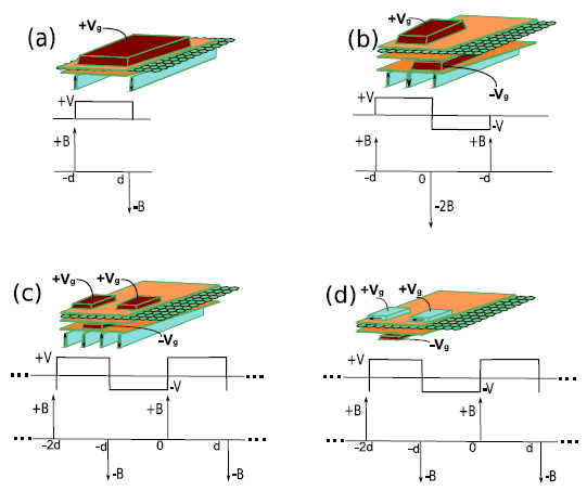
We first discuss briefly some of the practical issues when a electrostatic gate potential is applied to the graphene sheet. A gate voltage can be applied using a metal electrode and separating the electrode from the graphene layer with an insulating oxide layer. This oxide layer which serves as a dielectric medium between graphene sheet and metal electrode can be made as thin as several nanometers. When such a voltage is applied locally, it induces electron (hole) doping proportionally and changes the carrier concentration within the channel. This shifts the undoped Fermi level from the Dirac point by an amount , where is the sign of the induced charge. Due to this a local potential barrier V is created which is equal to the difference between the local Fermi level and the Fermi level in the undoped region. Since the typical breakdown strength of dielectrics such as alumina and fused silica are around , a graphene layer could be subjected to 1V applied across a 100nm thick dielectric. Following Refs.KSN1 ; KSN2 , gate voltages of upto have already been applied to graphene flakes. The electrostatic gate potentials would be generally applied by separate conductors placed suitably in different planes than the FM stripes, but in some cases, the FM stripes could also be used to apply voltages.
IV.2.1 Electron optics with EMVP barrier
Below we discuss the transport in the presence of a single MVP barrier and a commensurate electrostatic step potential (EMVP) barrier.
| (25) |
We assume and set the incident energy at , where is the Fermi level located at the charge-neutral Dirac point in monolayer graphene and the voltage V is measured with respect to . The entire treatment that follows is applicable in the neighbourhood of the charge-neutral Dirac points as long as the dispersion remains linear. In addition, we also assume that scattering by an EMVP barrier is not strong enough to break the degeneracy of the K and points. In the region at either of the K points, the motion will be described by
| (26) |
Here . In the Landau gauge, the stationary solutions can again be written as
Substituting this in Eq.26, we get the following coupled equations
| (27) |
The above equation can be decoupled to yield
| (28) |
The corresponding stationary solutions are
| (29) |
| (30) |
These are similar in form to those for a pure magnetic barrier or an electrostatic step potential 10. But and , namely the and components of the wavevector inside and outside the barrier regime are different. Here, are in the respective regions. Upon setting incident energy as , substitution of Eqns.(29) and (30) in Eq.(28) leads to
| (31) |
The incidence angle and the refraction angle are given by and respectively. Eq.(31) can then be rewritten to obtain the Snell’s law analogue for electron waves of such massless Dirac fermions incident on the EMVP barrier as
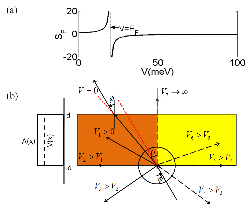
Comparison between Eq.(23) and Eq.(IV.2.1) shows that the potential barrier effectively scales the refraction angle by the scale factor defined above. is a non-monotonic and discontinuous function of [Fig.10(a)] and we shall study its impact on the refraction of the incident electron wave. There are basically two regimes to be analysed depending upon the strength of electrostatic potential applied (i) , (ii) . For positive incidence angles , in the absence of any electrostatic potential the refraction angle is larger than the incidence angle , thus the electrons are seen as passing from denser to rarer medium. As V increases from to , the function and hence increases continuously (this is shown in fig.10(a) and (b) respectively) and eventually the electron wave suffers TIR as soon as the r.h.s of Eq. IV.2.1 becomes greater than 1. Thus, by increasing V it is possible to totally reflect an electron wave for any given and . Since the reflectivity of a magnetic barrier increases with higher , this implies that the addition of can effectively convert a weaker magnetic barrier into a stronger one. This effective control of the strength of the magnetic barrier by an electrostatic potential ( gate voltage) is a consequence of the ultrarelativistic nature of the charge carriers in graphene. In a subsequent section we shall provide a more formal reasoning for this feature.
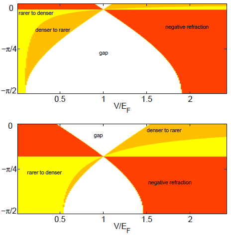
When V surpasses , the sign of will be opposite to the sign of . At smaller V close to there is still TIR, whereas for very high V much above the refraction becomes negative and the wave again retraces its path back in the barrier regime. This situation is depicted in Fig. 10(b), where the wavevector for the refracted ray is shown changing with increasing V. A similar analysis can be done for negative incidence angles. We summarize this discussion by plotting as a function of the incidence angle for different V and B values in Fig. 11. As can be seen, each of Fig.11(a) and (b) are separated into an upper and a lower part by the line . In the lower part where is larger than , with increasing the absolute value of the refracted angle, exhibits four phase regions: rarer denser, denser rarer, TIR gap, negative refraction. In the upper part, the four phase regions exhibit a different order with increasing : negative refraction, TIR gap, denser rarer, rarer denser. All these different regions meet at the limiting point , where the behaviour is singular and is discussed later on in this article in more detail.
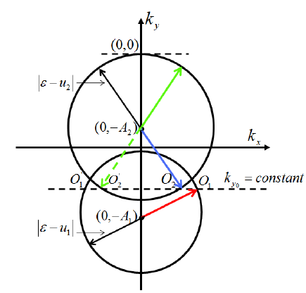
The refraction laws for the electron waves incident on an MVP/EMVP barrier can be alternatively understood with the following geometric considerationnori . We consider two domains with scalar and vector potential and respectively. The electron wave being incident from domain 1 at an angle and refracted in domain 2 at angle . Then the parallel and perpendicular wavevector components in domain 1 and 2 are related by the following dimensionless dispersion relations:
| (33) |
Each of the eq. 33 represents a circle in the plane, so that the wavevector for the propagating solutions will lie on the circle itself. Now, the refraction laws can be easily derived from fig.12 as follows. Due to translational invariance along the y-direction, the perpendicular wavevector component takes the same value in both domains . For a given , propagating solution in domain 1 and 2 will take the value which lie at the intersection of line with the corresponding circles. There are two such intersections for each of the circle. (This is shown in figure at and ). The physically meaningful intersection will be determined by the sign of . For definiteness we assume the incident current density to be positive i.e. . Then using the parametrization , will be positive or negative when respectively. This means the incident wave will be directed along the vector joining the centre of circle with when or opposite to the vector joining the centre of circle with when . Similarly, using the parametrization , the refracted current (which should possess the same sign as the incident current density) will be directed along the radius vector from the centre of the circle to the intersection point when , or opposite to the radius vector from the centre of the circle to when . Simple geometry from the fig.12 gives the following relation that defines the connection between the incident and refracted angles
This relation gives the same condition as in eq. IV.2.1 for EMVP barrier.
IV.2.2 EMVP barrier: Transmission probability
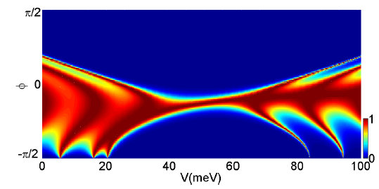
Transmission through a magnetic barrier gets strongly affected due to the presence of . Again from the continuity at in Eqs.(29) and (30), the transmission coefficient can be obtained as
| (34) |
where and . Here s and corresponds to sgn(E) and sgn(E-V) respectively. The expression for is same as the one for electrostatic potential barrier 11 or MVP barrier. However the difference in the result is due to the change in the expression for , namely the -component of the wave vector inside the barrier regime. In fig.13 is plotted transmittance as a function of and in the presence of an EMVP barrier. When the potential is lesser than but close to Fermi energy, transmission takes place over a very small window located asymmetrically along the axis. As the point is crossed, the function changes sign thereby changing the sign of refraction angle. Thus, the potential barrier induces more asymmetry in the transmission as against pure MVP barrier, this is clearly depicted in Fig. 13.
The point represents a singularity in the spectrum and demands a separate discussion. In the absence of magnetic barriers, such a point represents the zero modes for Dirac operators and leads to the emergence of new Dirac points. This has been discussed in a number of recent works considering Andreev Reflection in a graphene based NIS junction Shubhro and for electronic states of graphene in a periodic potential Brey ; CHPark2 ; CHPark3 . The presence of a magnetic barrier breaks the time reversal symmetry explicitly and these zero modes become the zero modes of the modified Dirac operator and the corresponding solutions are different. The equations satisfied by are
for which the solutions are obtained as
By using the continuity condition at , the transmission expression is obtained to be
The significance of such zero modes is that on the two sides of the singular point, the relative sign between the and becomes opposite.
IV.2.3 Conductance: Effect of various EMVP Barriers on Transport
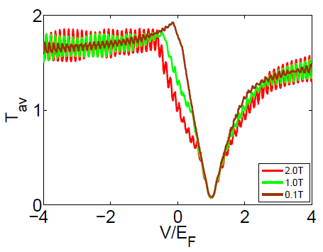
To see how the above angle-dependent transmission properties effect electron transport through such barriers, we plott the average transmission through the barrier as a function of the potential at various strengths of the magnetic barrier. The average transmission at a given barrier strength and is defined as Masir1
| (35) |
This formula, when generalized to a range of energy levels, leads to the Landauer conductance . This has been plotted for three different strengths of magnetic barrier over a range of potential barrier strength for a single EMVP barrier in Fig. 14. The transmission shows a minimum as expected when the point is approached. The transmission grows on both side of this singular point and finally at higher oscillates around an average value.
IV.2.4 Generalisation to MVP/EMVP barriers of any arbitrary shape
A general algorithm for the calculation of electron transmission in graphene through inhomogeneous electric and magnetic fields of any abitrary profile has been carried out in sameer using transfer matrix method. The fields are invariant in one direction; and the method involves the division of the one-dimensional domain into slices and taking an appropriate approximation of potential form in each slice. The equation for each slice is solved and the continuity conditions are used at the interfaces of two such slices. The exact solution of the equation in each slice depends on the potential form chosen. It is shown that in the presence of piecewise constant scalar potential and piecewise linear vector potential the resulting equation admits parabolic cylindrical functions as the solution basis in moderate magnetic fields while the basis functions tend to complex exponentials in the presence of extremely small magnetic fields. Also it is shown that the localised charge distribution (electron and hole puddles) which arises due to the presence of disorder in graphene yacobi can be modelled as the charge as arising from a scalar potential distribution proportional to it. With this the transmission calculation corresponding to a one-dimensional potential extracted from the experimental data in ref. yacobi is presented. The transport analysis with magnetic barriers in which the edges are smoothed out have also been carried out milpas - where a hyperbolic profile has been chosen. Here the corresponding Dirac equation can be analysed within the formalism of supersymmetric quantum mechanics, and leads to an exactly solvable model. Also, exact solutions have been given for a Dirac electron in the presence of an exponentially decaying magnetic field tkghosh .
IV.3 Quantum Goos-Hänchen Shift in single MVP and EMVP barriers
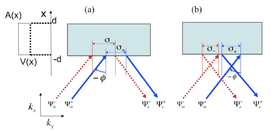
Analogues of optical phenomena such as refraction cheinov , collimation parknanolett , Fabry Perot interference peetersfabryperot , Bragg reflection sgms etc. in the ballistic transport regime for Dirac fermions in mono and bilayer graphene based structures in presence of scalar and vector potentials have been proposed. We discuss them in various sections of this review. In the following section we discuss another important optical phenomenon, the Goos-Hänchen (GH) effect GH ; Newton . The GH effect is a phenomenon of classical optics that describes the lateral shift between the centre of a reflected beam and that of incident beam when a total reflection occurs at the interface between two media. The shift occurs as the totally reflected ray undergoes a phase shift with respect to the incident beam, and this is is detectable since the extent of a real beam is always finite. The shift reverses sign if the second medium behaves like a metamaterial with negative refraction Berman ; Shadridov . Such a lateral shift for totally as well as partially reflected electron waves can also occur for non-relativistic electrons passing through a semiconductor barrier chen1 , magneto-electric semiconductor nanostructure chen2 . Recently, it has been shown that ballistic electrons passing through a p-n interface in graphene BeenakerGH also suffer a GH shift, which changes sign at certain angles of incidence. The analysis was extended for the case of MVP and EMVP barriers subsequently mssg . To understand GH shift in graphene, we consider the following wavepacket (beam) of electrons impinging on a p-n interface or a MVP/EMVP barrier at energy :
| (36) |
The envelope function ensures the wavepacket is of finite size along the -direction and is sharply peaked at . Thus, and the angle of incidence . This fact is represented by writing the x-component of wavevector, as well as both as function of in Eq.(36). We take a finite beam with a gaussian envelope such that
| (37) |
When , we can approximate the -dependent terms by a Taylor expansion around and retaining only the first order term to get
| (38) |
Substituting in Eq.(36) and integrating, we obtain
| (39) |
where
| (40) |
Here the primed quantities denote derivative taken wrt . Thus, upper and lower components of the spinorial wave function are localized at separate points along the -axis.
The reflected wavepacket can also be written in an analogous way by making the transformation to and to as well as multiplying the reflection amplitude . The reflected wave is then
| (41) |
Here again, . The spatial profile of the reflected wave can be again obtained by first expanding all dependent quantities around and retaining only the first order terms and then integrating in Eq.(41). This leads to
| (42) |
Here, and are given by
| (43) |
The above expression shows that the upper as well as lower components get shifted because of the phase factor. The GH shifts of the upper and lower components are respectively given by
| (44) |
Thus, the average shift for an MVP or EMVP barrier is
| (45) |
The situation is depicted schematically in Fig. 15. The last term in the above expression is a coordinate dependent quantity and will get an equal and opposite contribution from the term. The resultant will thus be independent of the choice of the coordinate of the interface from which TIR will take place.
IV.3.1 GH shift at p-n interface
To calculate the GH shift occuring at the p-n interface, we first require to calculate the gradient of the phase of the refletion coefficient, the negative of which gives the GH shift. For this we match the wavefunctions at the interface of the barrier such that the propagating wavefunction on the left of the interface should match with the evanescent wavefunction at the right of the interface.
| (46) |
| (47) |
Here , and
TIR at p-n interface will take place when , for which the incidence angle lies in the range . The continuity of the wave function at gives the reflection coefficient as
| (48) |
Clearly, the phase of the reflection coefficient is . The GH shift can now be written as:
| (49) |
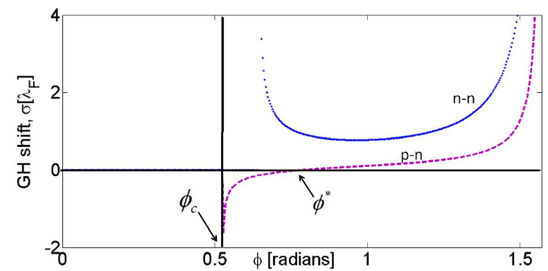
Using this expression, one can calculate the GH shift at p-n interface.
| (50) |
This is the same expression as the one obtained in BeenakerGH . Since for decaying evanescent solutions at the right of the p-n interface, for positive incidence angles the negative GH shift at the p-n interface will occur when . Thus, for angles of incidence , GH shift occurs in the backward direction. This is explicitly shown in fig.16.
IV.3.2 GH shift for MVP/EMVP barriers
For pure MVP barrier, TIR will take place when . This will happen when for and when for . In the latter case, this requires the wave vector to be negatively refracted at sufficiently high magnetic field before TIR occurs. This is already explained in section IV.1 in detail. The GH shift can then be obtained with the expression as in eq.49 with only
An EMVP barrier is essentially a p-n junction placed in a MVP barrier. For an EMVP barrier, TIR occurs for electrons incident from both sides of the surface normal but at different critical angles. For a given , it is possible to change adiabatically and get the electron wave reflected over a range of satisfying . We can keep fixed and increase . At , TIR occurs when giving
Upon further increasing , the electron wave remains totally reflected till reaches the second critical value such that giving
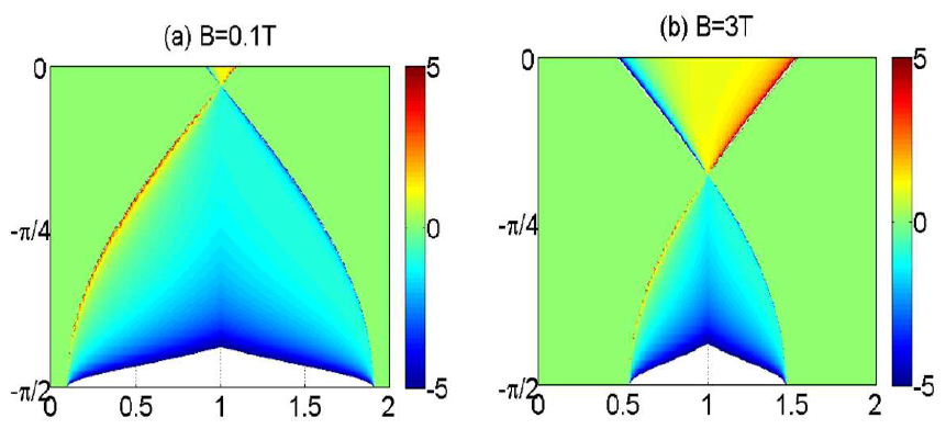
TIR occurs in the range . In Fig. 17 is plotted the GH shift over the entire range of and . At all other regions in the plane the GH shift is set to (green). The explicit expression for the GH shift for an EMVP barrier in dimensionless form is
| (51) |
The term in the numerator which is or diverges at the critical angle for TIR and leads to a divergent GH shift. This is because just at the critical angle the wavevector lies in the interface of the two regions. As a result in Fig. 17, the border TIR region of finite GH shift shows the highest GH shift.
The upper and lower parts of the curve are again separated by the line . The left and right boundaries correspond to and . In the lower part, the GH shift is mostly negative with the left and right boundaries having positive and negative refraction respectively.
Comparing Eq.(51) with Eq. (50), we see that . This is due to the non-specular nature of electron refraction at an EMVP barrier. This is an important difference in the quantum GH effect that occurs upon TIR by an EMVP barrier as compared to TIR by a purely electrostatic barrier for which as can be seen from Eq.50.
IV.3.3 Lateral shift in the transmitted wave
As explained in the previous section, Goos-Hänchen shift is analogous to the phenomenon of the lateral shift of the light beam total internally reflected from dielectric surface. Chen et al. chen1 ; chen2 investigated the lateral shifts for Dirac fermions in transmission through monolayer graphene barrier, based on tunable transmission gap. This shift has same physical origin that is due to the beam reshaping since each plane wave component undergoes different phase shift, however it has nothing to do with the evanescent waves which plays an all important role in the lateral shift of total internally reflected wavefunction. For this reason this shift can be termed as Goos-Hänchen like (GHL) shift and can be considered as an electronic analogue of the lateral shifts of light beam transmitted through a metamaterial slab.
According to stationary phase approximation stationaryphase and on the same lines as explained for GH shift for the reflected beam in th previous section, the GHL shifts of the transmitted beam through a barrier in graphene can be obtained as chen1 ; chen2 where refers to the phase of the transmission amplitude and the subscript corresponds to the wavevector at central incidence angle. Using (11), and assuming the form , the transmission phase is obtained as
so that
| (52) |
, where .
Since the product appears in the GHL shift expression so the analysis of the expression can be classified into (Klein tunneling regime) and (classical motion regime).
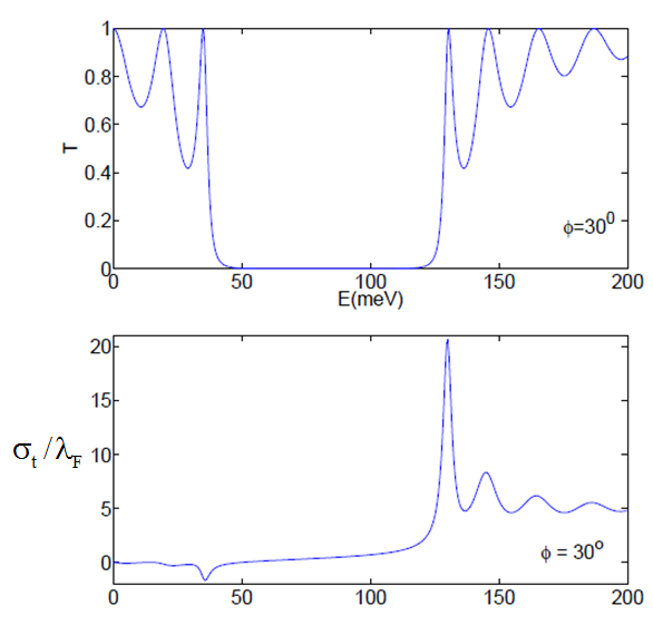
In the regime when , (for and for all values of incident energy, E). Then in accordance with (52), the maximum absolute value GHL shift corresponds to (These wavevector also corresponds to transmission resonances). Hence
Thus in Klein tunneling regime, the GHL shifts are negative shifts when .
In the other regime when , (for and for all values of incident energy, E). Then in accordance with (52), the maximum absolute value of GHL shift corresponds to (This wavevector also corresponds to transmission resonances). Hence
Thus in classical regime, the GHL shifts are always positive.
Thus we see that the GHL shifts in transmission can be negative or positive, and can be enhanced by the transmission resonances when the incidence angle is less than the critical angle for total reflection. This is clearly depicted in Fig.18.
IV.4 Fabry-Perot Interference in Graphene Heterojunctions: Effect of magnetic field
Another important optical analogue that can be studied in the ballistic transport regime of graphene is the formation of Fabry-Perot resonances. Study of such resonances is the linear and non-linear transport regime for non relativistic electrons for devices such as resonant tunnelling diodes is well known for a long time particularly after the pioneering work by Esaki ; dutta . A excellent review on the experimental progress on such resonances in graphene based heterostructures in the ballistic transport regime can be found in Youngreview .
Below we revisit the analysis of potential barrier as a Fabry-Perot interferometer peetersfabryperot ; shytov and then we analyse that how the FP resonances get effected in the presence of magnetic field in graphene.
The two edges of the square potential barrier acts as the two interfaces of FP interferometer peetersfabryperot , as shown in Fig. 20. As an electron wave is incident on the potential barrier at an angle , it splits into the transmitted wave and reflected wave at the left edge . The transmitted wave propagate further to suffer another reflection(transmission) at the right edge . In this way it gets multiply reflected between the two edges of the barrier. The difference in the optical paths between the transmitted wave and which suffer consecutive reflections at the right interface is given as
This means that the net phase difference between and is .
Again we introduce and to be the reflection and transmission coefficient for the potential step outside the barrier, and and the corresponding coefficients for inside the barrier. In analogy with the optical waves, net transmission through the barrier is obtained as
.
Then, the total transmission probability is obtained as
| (53) |
Proceeding with the calculation given in section 2, the reflection and transmission coefficients , , and can be obtained by matching the wavefunction at the interface of the potential step.
Matching conditions at gives
| (54) |
Substituting 54 in 53 we obtain the total transmission probability of a single barrier.
Clearly the transmission resonances which are also the Fabry perot resonances occur at . The energies at which these resonance occur are obtained as:
| (55) |
Also T is equal to 1 at normal incidence .
To show the effect of magnetic field which is already mentioned in sectionII.2 explicitly, we consider a potential barrier of height with a commensurate magnetic field peetersfabryperot
| (56) |
With the similar analysis as in section III.2, the carriers in the presence of such potential form, obey the Schrdinger like equation of the form:
Upon solving, the solutions can be obtained as:
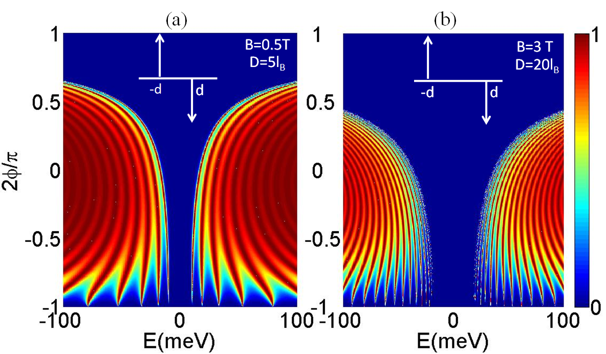
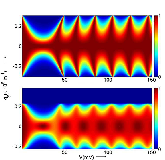
The solutions in the outside regions namely remain same as in section III.2. By using the continuity condition to match the wavefunctions at the boundaries of the barrier we numerically evaluate the transmission as plotted in fig.19. Since in the presence of magnetic field the y-component of the momentum varies inside the barrier as , so the for the incidence angles at the two interfaces 1 and 2 to be of equal sign, and should have opposite signs ie.
This gives the following condition on the y-component of momentum:
A fringe contrast from color minimum of transmission to the color maximum of the transmission on the two sides of the lines at can be clearly seen in the Fig.19 which occurs as a consequence of the half a period shift in the transmission resonances. Occurance of such phase shift for charge carriers in graphene was originally studied for a harmonic potential in a uniform magnetic field by Shytov et al. shytov and used as an experimental signature of Klein tunnelling kleinexp . This has already been discussed in section II.2. Transmission and conductance of massless Dirac fermions in the presence of multiple, disordered short range scatterers can also be understood in terms of resonant transport through double barrier structure. This has been discussed in detail in Ref. neetugreen .
V Periodic lattice of MVP barriers
Electron transport in graphene in presence of superlattices formed with electrostatic potential or magnetic barriers lead to large a body work in recent timesperiodic6 ; sgms ; mssg ; Martino ; fractal1 . They lead to interesting physics and potent with the possibility of creating new devices in the ballistic transport regime since they significantly alter the band structure. On other hand they resemble closely the phenomena of light propagation through medium with periodically modulated refractive index/dielectric constant which has been studied in detail in optics literature and also led to many important applications yariv ; kty . In the following section we discuss this type of transport and their consequences. We shall also discuss the emergence of additional dirac points in these modified band structure and the resulting collimation of transport electrons using such superlattice structure.
V.1 Bandstructure modification
In the previous section we have shown how MVP/EMVP barrier affects the ballistic transport in a profound way. Thus it will be interesting to find out how a periodic arrangement of these barriers will effect the transport, what is the resulting band structure etc.. As mentioned earlier, it has a direct optical analogue, namely with the electromagnetic propagation in periodic stratified media following the pioneering work by Yariv and collaborators yariv . It also provides us relativistic version of ordinary Kronig-Penny model and its magnetic counterpart.
Practically there will only be a finite number of barriers present in the system and the lattice translational symmetry will break down at the boundaries. However to simplify the analysis, we assume that the unit structure- a double EMVP barrier structure can be repeated infinitely along the -axis. The magnetic field creating such a barrier together with a superimposed splitgate voltage geometry, hence forth will be called DEMVP barrier. Since changing or reversing can locally convert a charge-neutral region into a p-n or n-p junction, such a periodic barrier can also be thought of as a semiconductor heterostructure. It should be emphasized that this can lead to new device structures due to combined effect of the highly inhomogeneous and periodic magnetic fields and controllable voltages. The vector and scalar potentials are characterized by
| (57) |
The schematic diagram in Fig. 9(b) shows how such DEMVP barriers can be constructed by placing metal electrodes and insulating layers between PMA materials with alternating magnetizations and the graphene sheet.
We consider each unit cell of size for the MVP as well as for the electrostatic potential barriers. Thus, the n-th cell is given by the region between and . In the -th part of a unit cell, the wavefunction is
| (58) | |||||
Here,
| (59) |
The wavevectors are given as
The exponential factor reveals the existence of lattice translational symmetry, which is not present for the isolated EMVP and DEMVP barriers.
The continuity of the wavefunction at the first interface at gives
| (60) |
Similarly, the continuity at the second interface at gives
| (61) |
Introducing a shorthand notations like,
The above two matrix equations can be combined as
| (63) |
According to Bloch theorem,
| (64) |
The matrix is unimodular. From Eqs.(63) and (64) we obtain the eigenvalue equation
| (65) |
where is the Bloch momentum. The complex conjugate eigenvalues are given by .This implies , which finally gives
| (66) |
Writing in terms of the wavevectors and the angles , the above eigenvalue condition reads
| (67) |
This equation provides the band structure for a periodic DEMVP barrier superlattice in general for any . By substituting in the above expression, the band structure for a periodic DMVP barrier superlattice can be obtained. This is an extension of the Kronig-Penney (KP) model to two-dimensional massless Dirac fermions. Thus, it is interesting to compare the DEMVP band structure with other variants of the KP model. The original KP model describes Bloch waves in a one-dimensional periodic potential Kittel . Several authors have also studied the relativistic KP model periodic1 ; periodic2 ; periodic4 ; periodic5 , where the motion considered is strictly one-dimensional. The non-relativistic KP model in periodic structures created by MVP barriers has also been studied peetersprl ; periodic3 . For graphene charge carriers, such problems have also been studied for different types of periodic magnetic sgms ; mssg ; Martino ; fractal1 as well as electrostatic periodic6 barriers. Magnetotransport studies in presence of periodic barriers Nasir where the periodic modulation is sinusoidal was carried out for monolayer graphene and it was found that such periodic modulations Landau levels into bands which oscillate with the strength of the magnetic field.
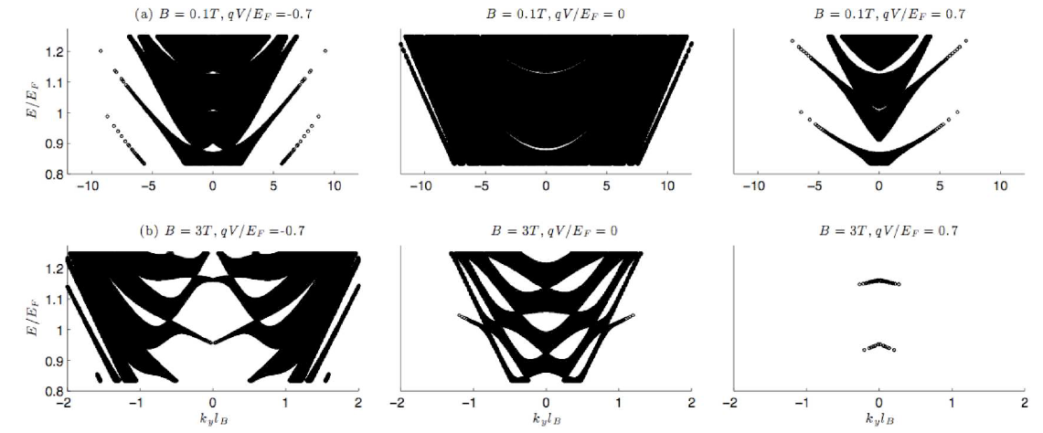
In Fig. 21 is plotted the band structure of corresponding to the periodic DEMVP barriers as a function of magnetic field and voltage . Conducting regions are seen over a wide range of with forbidden regions in between. At T, the region near is mostly conducting for different values of energy where a forbidden region starts opening up both to the left and right of the axis. The gaps are much wider than their counterparts for pure MVP barriers. Close to , an extended forbidden zone appears. To understand more explicitly, the band structure is also plotted at close to the singular point.
Here, the conducting regions are intervened by large patches of forbidden zones. In comparison, at , the behaviour is completely changed and the forbidden zone over the same range of shrinks considerably (left column). For higher where , the system is conducting at almost all . At T and near zero , a forbidden region opens up at various values of the energy and is much larger than at T. The gapped regions to the left and right of zero at T are located in a pronounced asymmetric manner as compared to when T. This asymmetry in the band structure as a function of as well as the opening up of large forbidden zones for certain values of differentiates the transport through EMVP barriers from MVP barriers and thus, it provides more flexibility to tune such transport.
As shown by various studies, carriers in graphene superlattices exhibit several interesting features parknat Bliokh parknanolett that result from the particular electronic SL band structure. Below we briefly analyse the bandstructure of periodic DMVP barrier superlattice.
V.1.1 Dispersion in the vicinity of neutrality point
We begin with analysing the dispersion relation in the vicinity of the neutrality point i.e.. close to zero energy. By rewriting the Eq.67 in the form of , then expanding the -function to the lowest order in and and then in in the vicinity of the neutrality point , we obtain the dispersion relation:
| (68) |
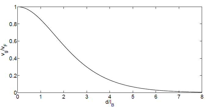
Clearly, the above dispersion relation is isotropic with zero gap between the valence band and conduction band. Moreover the group velocity depends on the width of the unit DMVP barrier as well as on the field strength. The group velocity is plotted in Fig. 22, which clearly shows that is always smaller than the Fermi velocity and it monotonously decreases for increasing , which is implied from the single MVP barrier analysis as well.
V.1.2 finite energy Dirac points
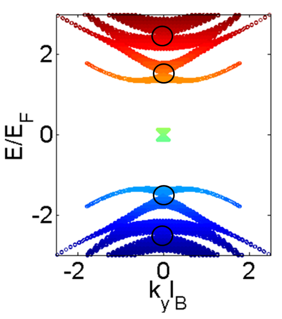
Apart from the neutrality point described in Eq. 68, many other degeneracy points can be seen in Fig.23 where the dispersion have a double cone like structure. The locations of these points occuring along the direction can be obtained analytically as
| (69) |
Again by expnading the -function in the vicinity of these points , the dispersion relation is obtained as
| (70) |
with the group velocity components given by
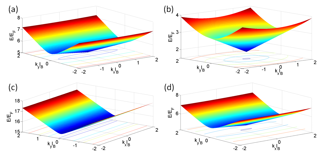
Clearly the dispersion relation is linear in and , which shows that in the presence of DMVP barrier superlattice, there are infinite number of degeneracy points close to which the dispersion has a double cone shape which is asymmetric in and direction. These points are termed as ”Extra Dirac points” in literatureana nygen .
In contrast to the dispersion relation at the neutrality point which is isotropic in nature, the dispersion at these finite energy extra Dirac points is anisotropic . As determined by Eq.70, we plot in Fig.24, the dispersion relation at for different field strengths, . From this we infer a collimation along direction ie. and as the contours become almost independent of . This is similar to that found for a superlattice of electrostatic potential barriers parknanolett .
VI The transformation of Magnetic to Electric Field for dirac fermions in graphene: a case for relativistic invariance
For the electron transport in presence of a transverse uniform magnetic field it was shown by Lukose et al. lukose that the Landau levels gets modified when the system is subjected to an electric field, finally leading to the Landau level collapse through the renormalization of the cyclotron frequency. A similar rescaling of the magnetic field strength took place when a suitable gate voltage is applied for the magnetic barrier problem as well mssg as discussed in section IV.2. To summarize one can change the strength of a magnetic field by suitably applying a get voltage. A more detailed analysis done later on tan how the relativistic invariance of the effective equation that governs the charge carriers in graphene leads to this interconvertibility of electric and magnetic field. In this section we shall describe this approach.
According to Special theory of Relativity, the laws of physics must be formed in a form so that it do not allow one to distinguish between the frames of reference which are moving with a constant relative velocity. The transformation between such frames are described by Lorentz transfromations. Like Maxwell’s equations, Dirac equation is also Lorentz covariant.
So, for the charge carriers in graphene obeying ”Dirac-like” equation, the Lorentz covariant structure of Hamlitonian can be used to find an analogy with special relativity. The analogy extends to problems involving coupling of electrons to external electric or magnetic fields. It is known from from special Relativity that in the presence of electromagnetic fields there are two invariants; namely and which remain unchanged in transition from one inertial frame to another landaulif . This means, by means of Lorentz transformation we can always give and any arbitrary values, subject to only condition that and have fixed values. Particularly, if , then we can always find a reference frame in which or (according as or , ie. the field is purely electric or purely magnetic. In the following discussion we’ll first find the transformation laws for the graphene charge carriers and then we analyse the consequences of application of Lorentz boost lukose ; tan ; shytovguthesispaper . For this, it will be convenient to write graphene equation in Lorentz - covariant form shytovguthesispaper :
| (71) |
where the matrices satisfy the anticommutation relation ; is the metric -tensor. We can explitly write the gamma-matrices as: , , , where are Pauli matrices. Here we use the space-time notation for coordinates as , momenta , and external field .
The above Eq.71 is invariant under Lorentz transformation. The transformation laws can be obtained on the same lines as for the general Dirac equation. The space-time coordinates, momenta and fields transform as:
| (72) | |||||
where for .
We consider the magnetic field modulations where the field strengths vary in direction and are constant in y-direction and scalar potential V = V(x), then in Eq.71. Writing the solutions as , we obtain
| (73) |
Now we apply two set of transformations tan (A) a lorentz boost in y direction with rapidity , followed by (B) a reflection about the y-axis. These two transformations together make a complex Lorentz boost as . With this complex Lorentz boost applied the energy and momentum transforms as :
And transformed Eq. 73 becomes
| (74) |
On comparing 73 and 74 it can be clearly seen that it is the imaginary scalar potential which is now coupling with the y-component of momentum and the role of scalar potential is now played by the external vector potential (again imaginary).
This section concludes our reviewing various aspects of ballistic electron transport in monolayer graphene through magnetic barriers, tuned by gate voltage and the associated optical analogy. In the subsequent section we shall discuss the electron transport in bilayer graphene in presence of such magnetic barriers.
VII Magnetic barriers in bilayer graphene
VII.1 Transmission through magnetic barriers
In this section, we consider the effect of such inhomogenous magnetic fields for the case of unbiased bilayer graphene (BLG). Bilayer graphene is modelled as two coupled hexagonal lattices including inequivalent sites and in the bottom and top layers respectively. The present work discusses bilayer graphene in bernal stacking. In such an arrangement, the bottom and top layers are shifted with respect to each other in such a manner that sites are exactly above the sites and sites are exactly in the middle of the hexagons of the bottom layer. In addition to intralayer interactions, there are interlayer interactions present in the system. The band structure is derived after taking into account two possible ways of hopping asymfalco : via the dimer state or due to weak but direct coupling. There are other weaker tunnelling processes dressdress which are neglected in this tight-binding approximation which we consider. The tight-binding Hamiltonian asymfalco derived in this way spans over the basis states that are located at . The effective low energy Hamiltonian near the Fermi level asymfalco obtained within the approximation from this tight binding Hamiltonian in this case is different from the corresponding one given in Eq.(5) for monolayer graphene.
The effective Hamiltonian is given as
The solutions of these equations are massive Dirac fermions since they have a quadratic dispersion and non-zero effective mass m. The applicability of this model Hamiltonian to study transport through a scalar potential was discussed in detail in poole . In the presence of scalar potential , under normal incidence , pseudospin is still conserved, but the Hamiltonian is like that of a Schrdinger particle; i.e., . The probability amplitude of corresponding charge carriers exponentially decays like usual Schrdinger particles inside the barrier leading to negligible transmission KSN3 ; todorovskiy ; parkprb84 . Drawing an analogy with optical transmission we call this phenomenon Klein reflection.
Below we calculate the effect of magnetic barrier for the case of bilayer graphene (BLG). The electronic wavefunction depends on the spatial profile of the vector potential and the boundary conditions when an electron is incident from a region with to a region where . We show this by explicitly calculating transmission by a transfer matrix approach masir , nilsson . Chiral charge carriers in BLG obey:
| (75) |
Here, they are described by a -component spinor and a Hamiltonian in the presence of a magnetic barrier and an electrostatic potential. with m/s and is the tunnel coupling between the two layers. and are the potentials at the two layers. The field profile taken here is . As pointed out earlier that such a sharp profile is routinely created in magnetic recording media where bit lengths can be varied over nm range using suitable domain engineering terris ; IEEE . Since this length scale is much larger than the A-A lattice constant of nm in graphene but also much smaller than the Fermi wavelength nm (at meV) of the incident electrons in bilayer graphene, the inhomogenous field pattern can be well approximated by the sharp edged profile proposed here. For bilayer graphene also, such sharp fields produced either by a patterned media layer or by a close-packed nanowire array can be easily integrated in the underlayer present in typical top- and bottom-gated graphene devices for Klein tunnelling studies kleinexp . The fields and voltages needed are within range of values already being used.
We are interested in the stationary state solutions of the form . Since , we can assume solutions like , for . Substituting this into Eq.75, and using and as units of length scale and energy scale respectively, to define the dimensionless quantities , , and , we obtain the following set of coupled equations:
| (76) |
Here
| (77) |
represents sign of , with and .
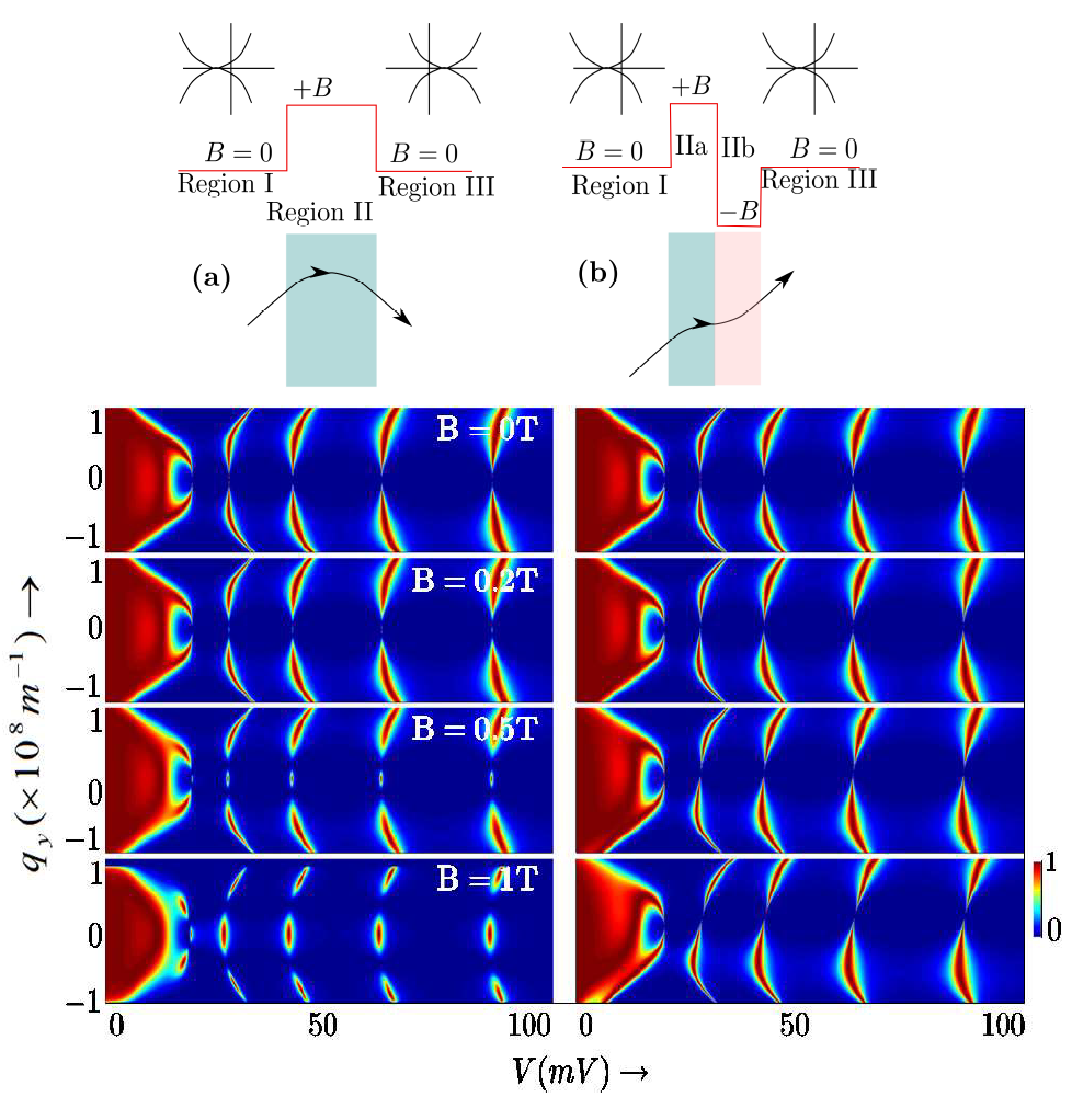
The solutions can be explicitly obtained in the three regions (region I), (region II) and (region III) as follows:
Region I() and III() are constant vector potential regions. We substitute in Eq.76. With this, the dispersion relation becomes:
| (78) |
Here, with . Also, is the total magnetic flux through an area in units of the flux quantum . The above Eq.78 leads to propagating as well as evanescent wave solutions. The unbiased BLG (which is the case considered here), corresponds to , and inregion I and III. Then the complete wave function in region I and III can be given as:
| (79) |
For the wavefunction solutions in region II, where the magnetic field is finite, we introduce and rewrite Eq.76 as:
| (80) |
With this, we obtain two coupled equations in and which looks like
| (81) |
The above two equations can be solved to obtain a fourth order differential equation which can be decomposed in two second order differential equations. For , we obtain :
| (82) |
The above equation admits the solutions which are of the form of parabolic cylindrical functions gradshteyn . For the case of unbiased BLG the complete wavefunction solution in region II can be given in terms of a compact matrix as:
Here D corresponds to parabolic cylindrical function of argument z and order . Also and , and . The current density expression is obtained as . The transfer matrix through any combination of a scalar and vector potential can now be written in terms of transfer matrices and for regions with finite and zero magnetic field respectively. This can then be used to find the transmission. The ratio of current density in region III and the incident current density in region I gives the transmission probability as a function of the angle of incidence .
In region I we parametrize in terms of incident energy, () and the angle of incidence as . In region III similar parametrization can be done in terms of the angle of emergence to write . The conservation of energy and constancy of the normal component of momentum then ensure
This equation explains that beyond a certain critical angle the electron beam and its cross-section (allowed values) is reduced with increasing barrier strength. This feature, along with chiral symmetry breaking, dictates the nature of transmission as is subsequently explained.
In figure 25 is plotted transmittance T for a magnetic barrier ((a), left column) and for a barrier well ((b), right column). In figure 1(a), the uppermost plot gives T for , clearly showing the region of perfect reflection around normal incidence symmetrically placed between two wings of resonant Fabry–Perot fringes. This is a generic feature of transmission through such barriers shytov masir . As the barrier strength increases to , a transmission region develops between these two wings due to the effect of the magnetic barrier and the resulting transmission also becomes asymmetric. For higher fields, the disappearance of perfect Klein reflection at normal incidence is seen even more clearly. We may then conclude that in BLG, though the passage from electron to hole states at normal incidence is usually forbidden due to pseudospin conservation, even a weak magnetic field lifts this restriction. For a weak magnetic field, the coupling between electron and hole states is also weak; however, for a case of resonant scattering one can expect total transmission nasgms The total angular range of transmission however shrinks in the presence of the magnetic barrier since, beyond a certain incident angle, all electron waves suffer total internal reflection. In figure 1(b) is plotted T through a barrier well, consisting of two magnetic barriers equal in magnitude and opposite in direction such that the total flux through the region vanishes. Now, the incident and the transmitted wavevectors are parallel to each other. As a result, the net rotation of the pseudospinor due to the inhomogeneous field vanishes and Klein reflection at normal incidence is restored. The Fabry–Perot fringes bend due to asymmetric transmission at a given V.
VII.2 Conductance
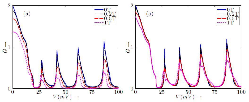
We now study the effect of the above transmission on conductance at very low temperatures and for energies close to the Fermi energy in the linear transport regime. To a good approximation, the dimensionless conductance can be written as Masir1
| (83) |
Fig.26 plots conductance as a function voltage. This shows that the gaps between the conductance maxima and minima get reduced in the presence of a magnetic barrier. The barrier reflects electrons incident upon it beyond a critical angle and the angular range of transmission shrinks with increasing barrier strength. As a result, the absolute value of conductance maxima comes down. Also the asymmetry, namely the way changes to the right and left side of such maxima, reduces in the presence of magnetic barrier. The behaviour of the conductance is strongly dependent on transmission resonances. To explain this behaviour, therefore we shall now model these numerically computed transmission resonances using a the Breit Wigner model breit
| (84) |
Such a form is valid near the transmission resonance. The above model has been widely used to model the transport due to resonant tunnelling in semiconductor structure dutta . Recently this model has been used to understand the cloaking phenomena in bilayer graphene rudner . Here are respectively the momentum dependent resonant energy and the resonance width.
Following the expression (78) in the absence of a magnetic field, the resonance energy and the resonance width can be assumed to have a quadratic dependence on the wavevector rudner . Thus and . The quadratic dependence of the resonant energy and the transmission width explains why the Fabry-Perot fringes of transmission resonance depicted in the left column of Fig. 27 are of convex shape. The asymmetry in the form of this fringes reflects themselves in the plot of the conductance again depicted in the left lower corner of Fig. 27, as one goes from the conductance peak to the left and right along the axis (effectively the voltage axis). In order to analyse the conductance peak, we evaluate the quantity , Here represents the conductance value at the peak, and represents the conductance value in its neighbourhood. Then,
On substituting the quadratic dependencies of reseonance energy and resonance width in the integral,
which upon solving gives:
| (85) |
Clearly shows the sqaure root sigularities at the conductance peak and the term appearing in the expression introduces the asymmetry on the two sides of resonance energy.
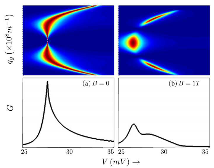
In the presence of a finite magnetic barrier, the small behaviour of such resonances can be obtained by using a semiclassical argument. We replace by its covariant form, namely . This yields where A is a constant. With increasing strength of the magnetic barrier, is shifted by the amount of the flux inserted in the barrier regime and this shift is independent of . The resonance width also follows a similar behaviour. The right column of figure 3 depicts this situation. The field-induced resonance leads to a central fringe symmetric about the voltage axis, unlike the upper and lower branches, which are asymmetric. This is again seen in the conductance plot as a right-left asymmetry around the conductance peak, which is now reduced. The reduction of the conductance peak can be attributed to the shrinking of the angular range of transmission due to the magnetic barrier, whereas the rounding of the conductance peak and the consequent reduction in the left and right asymmetry around this peak is an indicator of the reversal of Klein reflection. Since conductance is a physically measurable quantity, this provides a direct way to experimentally test our results.
VII.3 Generalisation beyond bilayer
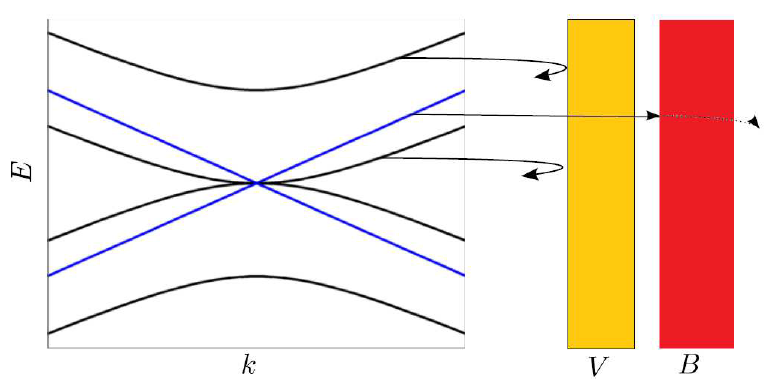
The above findings also extend to multilayer graphene. For N-layer graphene with Bernal () stacking The dispersion relation is given by min
where corresponds to the modes of the energy spectrum, is the Fermi velocity. For odd , is massless and it’s energy is given by
| (86) |
For all other cases the dispersion relation takes the form . In the limit the low energy spectrum for the -th massive mode is given as
where we define as the effective mass of the -th massive mode. Such band structure has been plotted in fig.28 for trilayer graphene. Now the transport electrons near the Fermi level will be a mixture of eigenmodes, one of which is a massless Dirac mode and the others are massive modes with different effective masses and also have a different chirality. These arguments extend to also. An extension of the semiclassical argument presented earlier therefore suggests the following possibility in the case of such multilayer graphene. When such a system is exposed to a scalar potential barrier, a normally incident massless mode will undergo Klein tunnelling, whereas in the case of a massive mode there will be exponentially decaying transmission. In contrast, a magnetic barrier will be highly reflective for a massless mode but will transmit normally incident electrons for massive modes. A typical situation has been depicted in fig.28. Since the low energy band structure decomposes into one massless and massive modes for N odd and only N massive modes for N even min , our results qualitatively suggest that a magnetic barrier can be used to selectively allow or partially filter out a mode.
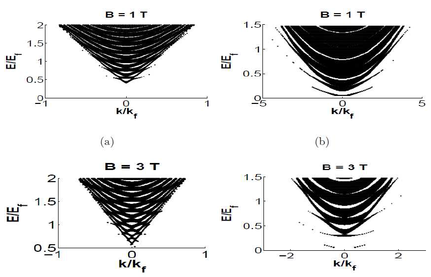
In Fig.29 we compare the modified bandstructure obtained with a periodic arrangement of DMVP in monolayer and bilayer graphene. One dimensional (1D) periodic modulation of the chemical potential or the electric field perpendicular to the layers was addressed in Ref. killi . For a periodic stratified media of several DMVP barriers, forbidden region appear in the bandstructure where the propagation of Bloch waves is not allowed. Th size of these forbidden regions increase with increasing strength of magnetic field. A comparison between the plots in Fig.29 (a),(c) and (b),(d) shows very clearly the conical band structure of monolayer graphene and parabolic bands in bilayer graphene.
This issue of anti-Klein tunnelling effect in bilayer graphene p-n-p junction and the effect of magnetic field on it, has also been addressed Ref. rudner . Here they describe it in terms of the bound states being completely decoupled from outside continuum states, thus calling it an electronic cloaking effect, and the barrier acting as ”cloak”. The effect is complete at normal incidence, leading to ”Klein reflection” or ”anti-Klein tunneling”. This is explained as follows: At normal incidence the effective equation that describes the motion of charge carriers in graphene , (as can be seen from Eq.75), can be analysed in the eigen basis of :
| (87) |
Clearly, the solutions for corresponds to the solutions outside the barrier. And the solution for (for which the equation appears with a negative sign) are bound state solutions, and corresponds to the solutions inside the barrier. Thus these two kinds of solutions are completely decoupled leading to zero transmission despite of the states available inside the barrier.
In section VII, our discussion on Klein reflection in bilayer graphene was based on the analysis of Fabry-Perot like transmission resonances developed from inhomogenous magnetic barriers in the presence of voltage. Here the oscillatory transmission due to Fabry-Perot like arises due to interference of forward and backward moving propagating waves which undergo multiple reflection between two interfaces. In addition to these FP like resonances a new kind of transmission resonances have also been seen for the case of gapped bilayer graphene nandkishore . In their recent work, R. Nandkishore et. al. proposed an entirely different approach to realize oscillatory transmission which involves only forward propagating waves and a single interface and thus is different from the FP resonances. They show that Zener transmission in a p-n junction in gapped bilayer graphene exhibits common path interference taking place under the tunnel barrier, leading to transmission that oscillates as a function of gate-tunable bandgap.The origin of this oscillatory behaviour lies in the fact that in the presence of p-n junction, bilayer graphene employs the propagating as well as evanescent wavevector solutions. The simultaneous existence of these two- leads to common path interference which gives rise to oscillatory transmission. These oscillations in transmission manifest themselves through negative differential conductivity in the characteristic. Interesting works were also done on pseudo spinotronics in biased bilayer graphene prada ; michetti which we shall not discuss in this review. Other recent developments made on these lines include the work by Campos et. al. trilayer , where they have realized giant conductance oscillations in ballistic trilayer graphene Fabry-Perot interferometers, which result from phase coherent transport through resonant bound states beneath an electrostatic barrier.
VIII Conclusion
A large body of work has followed since the proposal of using inhomogeneous magnetic fields in graphene and understanding the transport in an analogy with light beam propagation in optics- termed as electron optics. The similarities between polarization states of light and ballistic charge carriers in graphene has been investigated in detail in dragomanosa ; dragomanjosab29 . It is demonstrated theoretically dragomanjosab28 that regions with different electrostatic potentials in graphene can have the same transmission probability as the transmittance of layered structures in optics illuminated with normally incident TE waves if the incidence angle of electrons in graphene and the width of the gated region are appropriately chosen.This quantitative analogy can be useful for designing optical structures that correspond to graphene-based devices. Then there are proposals of electron waveguides created by electrostatic potential or by real magnetic barriers nori ; cesar . Here the control the of the quasiparticle flux in a graphene-based waveguide was theoretically investigated. Guided modes occuring in the negative-zero-positive index metamaterial waveguide ming and in symmetric velocity barrier jian , have also been investigated. It is shown that magnetically induced waveguide in graphene leads to strong confinement of Dirac fermions, regardless of its edge terminations myoung .The properties of unidirectional snake states have also been investigated in such waveguides tkghoshsnakestates . It was shown that for certain magnetic field profile, two spatially separated counterpropagating snake states are formed, leading to conductance quantization which is insensitive to backscattering by impurities or irregularities of the magnetic field.
It may be mentioned there are many other interesting articles in the relevant field and because of space restriction it is almost impossible to refer to all of them which we regret. We would also like to direct the readers some excellent reviews on electron transport in graphene where some of the related issues was discussed in somewhat different context. In ref. peresrevmodphy the transport properties of graphene that includes theoretical and experimental work was reviewed. In ref. norirev the charge and spin transport in mesoscopic graphene structures was reviewd in detail. In ref. dassharma the density and temperature-dependent charge transport in doped or gated graphene devices was reviewed. In ref. pereirarev ; fuchs the Klein tunnelling through single and multiple potential barriers was reviewed. Properties of graphene in presence of strong homegenous magnetic field was reviewed in ref. goerbig . Electronic properties of bilayer graphene was reviewed in detail in ref. mccann .
To summarize, We have reviewed several aspects of charge carrier transport in graphene through inhomogenous magnetic fields viz. magnetic barriers in detail. We reviewed experimental progress in designing such magnetic barriers at various length scales. Such barriers suppress Klein tunnelling, thereby achieving confinement in graphene, which can be seen through strong supression of transmission of electrons. We have shown that transport through MVP barriers can be understood in terms of propagation of light through periodic stratified media. This analogy can partially be attributed to the fact that equation describing Dirac like charge carriers in graphene and the Maxwell equations berreman are both linear wave equations. We show that such transport properties through a singular magnetic barrier can be much better controlled by the additional application of an electrostatic voltage. A detailed optical analogy for transport through single and multiple EMVP barriers arranged periodically was obtained highlighting optical analogues of phenomena such as TIR for positive and negative refraction and a Quantum Goos-Hänchen shift. One significant feature of such transport in this regime of the simultaneous application of highly inhomogenous magnetic fields along with electrostatic potentials, is highly anisotropic and strongly dependent on the sign of the voltage indicating possible device applications. We discuss collimation, emergence of extra dirac points in this context. We also reviewed transport through such magnetic barrier through unbiased graphene bilayer, describe reversal of Klein tunnelling, anticloaking, common path interference etc. in such systems. The wide range of optical analogues to charge transport in graphene may lead to practical devices such as Bragg reflectors, resonantors, waveguides etc. We hope this detailed review will augment theoretical and experimental research in this field.
IX Acknowledgements
We have benefited from discussions with many researchers including our students working on graphene in the last few years at various places. We particularly thank G. Bhaskaran, F. M. Peeters, R. Masir, M. Barbier, L. Levitov, R. Nandkishore, Leonardo Campos, Andrea Young, P. Michetti, V. Fal’ko, E. McCann, Mandar Deshmukh, K. Sengupta, Subhasis Ghosh, Sameer Grover, Sanjay Gupta, Nupur Gupta, V. Thareja for such discussions. We thank A. Nogaret and IOP Publishing for giving us the kind permission to use one the experimental figures published in ref. nogaretjpcm . This work is supported by grant SR/S2/CMP-0024/2009 from the Science and Engineering Research Council, DST, Government of India. NA is supported by a CSIR fellowship.
References
- (1) S. Datta, Electronic Transport in Mesoscopic Systems, Chapter 6 and 7, Cambridge University Press, (2005).
- (2) W. van Haeringen, D. Lenstra Analogies in Optics and Micro Electronics, Dordrecht: Kluwer, (1990).
- (3) P. Yeh, A. Yariv and C.S. Hong, J. Opt. Soc. Am., 67, 423 (1977) : A. Yariv and P. Yeh, Optical waves in crystals, Wiley Interscience, (2003).
- (4) C. Kittel, Introduction to Solid State Physics, th Ed., John Wiley and Sons Pte. Ltd., Singapore (1996).
- (5) U. Sivan, M. Heiblum, C. P. Umbach and H. Shtrikman, Phys. Rev. B 41, 7937 (1990).
- (6) J. Spector, H. L. Stormer, K. W. Baldwin, L. N. Pfeiffer and K. W. West, Appl. Phys. Lett. 56, 1290 (1990).
- (7) P. Wallace Phys.Rev. 71, 622 (1947).
- (8) K. S. Novoselov et al., Science, 306, 666, (2004).
- (9) K. S. Novoselov et al., Nature, 438, 197 (2005).
- (10) Y. Zhang et al., Nature, 438, 201 (2005).
- (11) V. V. Cheianov, V. Falko, B. L. Altshuler, Science 315, 1252 (2007).
- (12) V. G. Veselago, Sov. Phys. Usp. 10, 509 (1968).
- (13) J. B. Pendry, Phys. Rev. Lett.,85, 3966 (2000).
- (14) K. S. Novoselov et al., Nat. Phys., 2, 620 (2006).
- (15) A. F. Young and P. Kim, Ann. Rev. Cond. Matt. Phys. 2 1-20 (2010).
- (16) A. De Martino, L. Dell’Anna and R. Egger, Phys. Rev. Lett, 98, 066802 (2007).
- (17) A. Nogaret, J. Phys. Cond. Matt. 22, 253201 (2010).
- (18) J.Wro´bel et. al., Phys. Rev. Lett. 93, 246601 (2004 ).
- (19) S. Ghosh and M. Sharma, J. Phys. Cond. Matt. 21, 292204 (2009).
- (20) A. Matulis, F. M. Peeters and P. Vasilopoulos, Phys. Rev. Lett, 72, 1518 (1994).
- (21) M. Sharma and S. Ghosh, J. Phys. Cond. Matt. 23, 055501 (2011).
- (22) A. H. Castro Neto et al, Rev. Mod. Phys., 81, 109 (2009).
- (23) J. M. Pereira Jr et. al., Semicond. Sci. Technol. 25, 033002 (2010).
- (24) P. E. Allain and J. N. Fuchs Eur. Phys. J. B 83, 301 (2011)
- (25) R. Saito, G. Dresselhaus, and M.S. Dresselhaus Physical Properties of Carbon Nanotubes, Imperial College Press 1998.
- (26) M. S. Dresselhaus and G. Dresselhaus, Adv. Phys. 51 (2002) 1; R. C. Tatar and S. Rabii Phys. Rev. B 25, 4126 (1982) ; J. C. Charlier, X. Gonze, and J.-P. Michenaud Phys. Rev. B 43, 4579 (1991).
- (27) J. C. Slonczewski, P. R. Weiss, Phys. Rev. 109, 272 (1958).
- (28) G. W. Semenoff, Phys. Rev. Lett. 53, 2449 - 2452 (1984) .
- (29) F. D. M. Haldane, Phys. Rev. Lett. 61, 2015-2018 (1988).
- (30) A. Geim and K. S. Novoselov, Nat. Mater., 6, 183 (2007)
- (31) C. W. J. Beenakker, Rev. Mod. Phys., 80, 1337 (2008).
- (32) J. Cserti et. al., Phys. Rev. Lett. 99, 246801 (2007).
- (33) T. Ando, T. Nakanishi, J. Phys. Soc. Jpn. 67, 1704 (1998).
- (34) A. F. Young and P. Kim, Nat. Phys. 5, 222, (2009)
- (35) N. Stander, B. Huard, and D. Goldhaber-Gordon, Phys. Rev. Lett. 102, 026807 (2009).
- (36) G. A. Steele, G. Gotz and L. P. Kouwenhoven, Nat. Nano. 4, 363 (2009)
- (37) W. Greiner, Relativistic Quantum Mechanics, rd Ed., Springer (1997).
- (38) T. Tudorovskiy et al, Phys. Scr. 146T, 014010 (2012).
- (39) V. V. Cheianov and V. Falko, Phys. Rev. B, 74, 041403 (2006).
- (40) E. B. Sonin, Phys. Rev. B 79, 195438 (2009)
- (41) A. V. Shytov , M. S. Rudner and L. S. Levitov Phys. Rev. Lett. 101 156804 (2008).
- (42) S. Sutar, E. S. Comfort, J. Liu, T. Taniguchi, K. Watanabe, and J. U. Lee, Nano Lett. 12, 4460, (2012).
- (43) R. N. Sajjad, S. Sutar, J. U. Lee and A. W. Ghosh, Phys. Rev. B 86, 155412 (2012).
- (44) N. M. R. Peres, A. H. Castro Neto, and F. Guinea, Phys. Rev. B 73, 241403(R) (2006); P. G. Silvestrov and K. B. Efetov, Phys. Rev. Lett. 98, 016802 (2007).
- (45) B. Trauzettel and Denis V. Bulaev, D. Loss, and G. Burkard, Nat. Phys. 3, 192 (2007).
- (46) J. Milton Pereira, Jr., F. M. Peeters, and P. Vasilopoulos, Appl. Phys. Lett. 90, 132122 (2007).
- (47) J. Milton Pereira, Jr., P. Vasilopoulos, and F. M. Peeters, Nano Lett. 7, 946 (2007).
- (48) A. De Martino, L. Dell’Anna, and R. Egger, Solid State Commun. 144, 547 (2007).
- (49) S. Khizroev and D. Litvinov J. App. Phys. 95, 4521 (2004); M. Lu, L. Zhang, Y. Jin, and X. Yan, Eur. Phys. J. B 27, 565-70 (2002).
- (50) M. Albrecht et al. IEEE Trans. on Mag. 99, 2323 (2003).
- (51) A. Masseboeuf et al. Nano Lett., 9 (8), pp. 2803-2806 (2009).
- (52) W.A. Challener et al. Nat. Photon. 3, 220 (2009).
- (53) F. B. Mancoff, R. M. Clarke, C. M. Marcus, S. C. Zhang, K. Campman, and A. C. Gossard, Phys. Rev B 51, 13269 (1995); F. B. Mancoff, L. J. Zelinski, C. M. Marcus, K. Campman, and A. C. Gossard, ibid. 53, R7599 (1996); A. W. Rushforth, B.L. Gallagher, P. C. Main, A. C. Neumann, C. H. Marrows, I. Zoller, M. A. Howson, B. J. Hickey, and M. Henini, Physica E 6, 751 (2000).
- (54) S.J. Bending, K. von Kiitzing, and K. Ploog, Phys. Rev. Lett. 85, 1060 (1990).
- (55) A.K.Geim Pis’ma Zh. Eksp. Teor. Fiz. 50, 359 (1989) [JETP Lett. 50, 389 (1990)];
- (56) M. L. Leadbeater et al., Phys. Rev. B 52, R8629 (1995).
- (57) G. M. Gusev et al., Phys. Rev. B 53, 13641 (1996).
- (58) M. Grayson et al., Physica E 22, 181 (2004).
- (59) F. G. Monzon, M. Johnson, and M. L. Roukes, Appl. Phys. Lett. 71, 3087 (1997).
- (60) M. Johnson, B. R. Bennet, M. J. Yang, M. M. Miller, and B. V. Shangbrook, Appl. Phys. Lett. 71, 974 (1997).
- (61) V. Kubrak, A. C. Neumann, B. L. Gallagher, P. C. Main, M. Henini, C. H. Marrows, and M. A. Howson, Physica E 6, 755 (2000).
- (62) S. J. Lee, S. Souma, G. Ihm, and K. J. Chang, Phys. Rep. 394, 1 (2004).
- (63) F. M. Peeters and A. Matulis, Phys. Rev. B 48, 15166 (1993).
- (64) I. S. Ibrahim and F. M. Peeters, Am. J. Phys. 63, 171 (1995).
- (65) M. Johnson, B. R. Bennett, M. J. Yang, M. M. Miller, and B.V. Shanabrook, Appl. Phys. Lett. 71, 974 (1997); V. Kubrack et al., J. Appl. Phys. 87, 5986 (2000).
- (66) H. A. Carmona et al., Phys. Rev. Lett. 74, 3009 (1995); P. D. Ye et al., ibid. 74, 3013 (1995).
- (67) A. Nogaret, S. J. Bending, and M. Henini, Phys. Rev. Lett. 84, 2231 (2000).
- (68) K. S. Novoselov, A. K. Geim, S.V. Dubonos, Y. G. Cornelissens, F. M. Peeters, and J. C. Maan, Phys. Rev. B 65, 233312 (2002)
- (69) N.H. Shon and T. Ando, J. Phys. Soc. Jpn., 67, 2421 (1998).
- (70) I. S. Gradshteyn and I. M. Ryzhik, Table of Integrals, Series, and Product (New York: Academic) (1980).
- (71) J. K. You, L. Zhang L and P. K. Ghosh, 1995 Phys. Rev. B, 52, 17243 (1995); A. Majumder Phys. Rev. B 54, 11911 (1996); J. Reijniers J, F. M. Peeters, and A. Matulis, Phys. Rev. B 64, 245314 (2001); J. Reijniers and F. M. Peeters 2001 Phys. Rev. B 63, 165317 (2001);G. Papp, P. Vasilopoulos and F. M. Peeters, Phys. Rev. B 72, 115315 (2005).
- (72) N. Agrawal(Garg), S. Ghosh and M. Sharma, Proceeding of Indian national Science Academy, 77, 2 (2011).
- (73) M. R. Masir et al. Phys. Rev. B. 77, 235443 (2008).
- (74) M. Krawczyk and H. Puszkarski, Phys. Rev. B 77, 054437 (2008); S.D. Bader, Rev. Mod. Phys., 78, 1 (2006).
- (75) S.H. Sun et al, Science 287, 1989 (2000).
- (76) H. Zheng et al, Appl. Phys. Lett. 80, 2583 (2002).
- (77) K. von Bergmann et al, Phys. Rev. Lett. 96, 167203 (2006).
- (78) J. Martin et al., 2008, Nature Phys. 4, 144 (2008).
- (79) J. R. Williams et al, Science, 317, 5838, pp 638-641 (2007).
- (80) A. K. Bhatt et. al., Solid State Commun., 152, 545-548 (2012).
- (81) S. Pisana, P. Braganca, E. Marinero and B. Gurney, Nano Lett. 10, 341 (2010).
- (82) Y.P. Bliokh, V. Freilikher and F. Nori, Phys. Rev B 81, 075410 (2010)
- (83) S. Bhattacharjee, M. Maiti and K. Sengupta, Phys. Rev. B 76, 184514 (2007).
- (84) N. Agrawal, S. Ghosh and Manish Sharma, arXiv:1206.0249 [cond-mat.dis-nn]
- (85) L. Brey and H. A. Fertig, Phys. Rev. Lett. 103 046809, (2009).
- (86) C. H. Park, L. Yang, Y. W. Son, M. L. Cohen and S. G. Louie, Phys. Rev. Lett. 101, 126804 (2008).
- (87) C H Park, Y. W. Soon, L. Yang, M. L. Cohen and S. G. Louie, Phys. Rev. Lett.103, 046808 (2009).
- (88) S. Grover, S. Ghosh and M. Sharma, Modelling Simul. Mater. Sci. Eng. 20, 045010 (2012).
- (89) E. Milpas, M. Torres and G. Murgua, J. Phys. Cond. Matt. 23 245304 (2011).
- (90) T. K. Ghosh et al., Phys. Rev. B 77, 081404(R) (2008).
- (91) C.-H. Park, Y.-W. Son, L. Yang, M. L. Cohen, and S. G. Louie, Nano Lett. 8, 2920 (2008).
- (92) Masir. M. Ramezani, P. Vasilopoulos and F. M. Peeters, Phys. Rev. B 82 115417 (2010).
- (93) F. Goos and H. Hänchen, Ann. Phys. (Lpz.) 436 333-346 (1947).
- (94) de Fornel F 2001 Evanescent Waves: From Newtonian Optics to Atomic Optics (New York: Springer)
- (95) P. R. Berman, Phys. Rev. E 66, 067603 (2002).
- (96) I. V. Shadridov , A. A. Sukhorukov and Y. S. Kivshar Phys. Rev. Lett. 95, 193903 (2005)
- (97) X. Chen, C-F. Li and Y. Ban, Phys. Lett. A 354, 161 (2006); X. Chen X, Y. Ban Y and C-F. Li J. Appl. Phys. 105, 093710 (2009).
- (98) X. Chen, C-F. Li and Y. Ban Phys. Rev. B 77, 073307 (2008).
- (99) C. W. J. Beenakker, R. A. Sepkhanov and A. R. Akhmerov and J. Tworzydlo, Phys. Rev. Lett. 102, 146804 (2009).
- (100) D. Bohm, Quantum Theory, Prentice-Hall (New York, 1951), pp. 257−261
- (101) L. L. Chang, L. Esaki, and R. Tsu, Appl. Phys. Lett. 24, 593 (1974).
- (102) M. Barbier, P. Vasilopoulos, F. M. Peeters, and J. M. Pereira, Phys. Rev. B, 79, 155402 (2009).
- (103) L. Dell’Anna and A. D. Martino, Phys. Rev. B 79, 045420 (2009); See also the erratum at Phys. Rev. B 80, 089901(E) (2009).
- (104) L. Sun, C. Fang, and Y. Guo, J. Appl. Phys. 108, 063715 (2010); L. Sun, C. Fang, Y. Song and Y. Guo, J. Phys.: Cond. Matt. 22 445303 (2010).
- (105) A. K. Ghatak, K. Thyagarajan and M. R. Shenoy, IEEE J. Quant. Electron. 24, 1524 (1988).
- (106) B. H. J. Mckeller amd G. J. Stephenson, Jr., Phys. Rev. C 35, 2262 (1987).
- (107) B. Mendez, F. D. Adame and E. Maci, J. Phys. A: Math. Gen. 26, 171 (1993).
- (108) P. Strange, Relativistic Quantum Mechanics, Cambridge University Press, (1998).
- (109) M. Barbier, F. M. Peeters, P. Vasilopoulos and J. M. Pereira, Jr., Phys. Rev. B 77, 115446 (2008).
- (110) A. Krakovsky, Phys. Rev. B, 53, 8469, (1996).
- (111) R. Naseer, K. Sabeeh and M. Tahir, Phys. Rev. B 81, 085402 (2010).
- (112) C. H. Park et al, Nat. Phys., 4 3, 213-217 (2008)
- (113) Y. P. Bliokh et al, Phys. Rev. B, 79, 075123. (2009)
- (114) L. D. Anna and A. De. Martino, Phys. Rev. 83, 155449 (2011).
- (115) V. Q. Le et al., J. Phys. Condens. Matt. 24, 345502 (2012).
- (116) Vinu Lukose, R. Shankar, and G. Baskaran, Phys. Rev. Lett. 98, 116802 (2007).
- (117) L. Z. Tan, C. H. Park and S. G. Louie, Phys. Rev. B 81, 195426 (2010).
- (118) L. D. Landau and E. M. Lifshitz, Classical theory of fields, rd Ed., Pergamon, London (1971).
- (119) N. Gu et. al., Phys. Rev. Lett. 106, 066601 (2011).
- (120) E. McCann and V. I. Fal’ko, Phys. Rev. Lett. 96 086805 (2006) ; E. McCann, Phys. Rev. B 74 161403(R) (2006).
- (121) S. Park and H.-S. Sim, Phys. Rev. B 84, 235432 (2011)
- (122) C. J. Poole, Solid State Commun. 150, 632 (2010).
- (123) Masir. M. Ramezani, P. Vasilopoulos and F. M. Peeters, Phys. Rev. B 79, 035409 (2009); Masir. M. Ramezani et al, Appl. Phys. Lett. 93, 242103 (2008).
- (124) J. Nilsson et. al., Phys. Rev. B 76, 165416 (2007); M. Barbier, P. Vasilopoulos, F. M. Peeters and J. M. Pereira, Phys. Rev. B 79, 155402 (2009).
- (125) B. D. Terris and T Thomson, J. Phys. D: Appl. Phys. 38 R199 (2005).
- (126) N. Agrawal (Garg), S. Grover, S. Ghosh and M. Sharma, J. Phys. Cond. Matt. 24 175003 (2012).
- (127) G. Breit and E. Wigner, Phys. Rev. 49, 519 (1936).
- (128) N. Gu, M. Rudner and L. Levitov Phys. Rev. Lett. 107, 156603 (2011).
- (129) H. Min and A. H. MacDonald, Phys. Rev. B 77 155416 (2008); H. Min and A. H. MacDonald, Prog. Theor. Phys. Suppl. 176 227 (2008).
- (130) M. Killi et. al., Phys. Rev. Lett. 107, 086801 (2011); M. Barbier, P. Vasilopoulos, and F. M. Peeters, Phys. Rev. B 81, 075438 (2010); M. Barbier, P. Vasilopoulos, and F. M. Peeters, Phil. Trans. R. Soc. A 368, 5499 (2010).
- (131) R. Nandkishore and L. Levitov, Proc. Natl. Acad. Sci. 108, 14021 (2011).
- (132) P. San-Jose, E. Prada, E. McCann and H. Schomerus, Phys. Rev. Lett. 102, 247204 (2009)
- (133) P. Michetti et al, Nano Lett. 10, 4463 (2010)
- (134) L. C. Campos et. al., Nature Commun., 3, 1239 (2012).
- (135) D. Dragoman, J. Opt. Soc. Am., B 27, 1325 (2010).
- (136) I. Mihalache and D. Dragoman, J. Opt. Soc. Am., B, 28, 7, pg. 1746 (2011).
- (137) D. Dragoman, J. Opt. Soc. Am., B, 29, 6, pg. 1528 (2012).
- (138) C. E. P. Villegas and M. R. S. Tavares, App. Phys. Letts., 101, 163104 (2012).
- (139) T. K. Ghosh, Phys. Rev. B 77, 081404(R) (2008).
- (140) J-H. Yuan et. al., J. App. Phys., 110, 103706 (2011).
- (141) M. Shen et. al., Opt Exp. 18, 12779 (2010).
- (142) N. Myoung et. al., Phys. Rev. B 83, 113407 (2011).
- (143) D.W. Berreman, J. Opt. Soc. Am., 62, 502 (1972).
- (144) N. M. R. Peres, Rev. Mod. Phys. 82, 2673 (2010); N. M. R. Peres, J. Phys. Cond. Matt. 21 323201 (2009).
- (145) A.V. Rozhkov et. al., Physics Reports, 503, 77–114 (2011).
- (146) S. D. Sarma et. al., Rev. Mod. Phys. 83, 407 (2011).
- (147) M. O. Goerbig Rev. Mod. Phys. 83, 1193 (2011).
- (148) E. McCann and M. Koshino, arXiv:1205.6953 [cond-mat.mes-hall].
- (149) V. N. Kotov et. al., Rev. Mod. Phys. 84, 1067 (2012).
- (150) F. Molitor et. al., J. Phys. Cond. Matt. 23 243201 (2011).
- (151) F. Bonaccorso, Z. Sun, T. Hasan and A. C. Ferrari, Nature Photonics 4, 611 - 622 (2010).