Photoferroelectric solar to electrical conversion
Abstract
We propose a charge pump which converts solar energy into DC electricity. It is based on cyclic changes in the spontaneous electric polarization of a photoferroelectric material, which allows a transfer of charge from a low to a high voltage. To estimate the power efficiency we use a photoferroelectric liquid crystal as the working substance. For a specific choice of material, an efficiency of is obtained.
pacs:
61.30.Gd, 77.84.Nh, 77.80.B-, 84.60.Jt, 85.50.-n, 88.40.H-Photoferroelectrics are materials in which their ferroelectricity can be affected by exposure to light. We propose a device that works as a charge pump based on the photoferroelectric effect. Varying light intensity cycles a photoferroelectric working material through various electric polarization states and the associated charge in the external circuit is pumped from low to high potential.
A body with a uniform (ferroelectric) polarization has zero polarization charge density in the bulk, , while the surface charge density associated with the change of polarization from its finite bulk value to zero on traversing the surface cutting is given by . Figure 1 shows this associated with truncating . Such a layer of charge creates an internal electric field in the material in this slab geometry, where is the relative dielectric constant of the material. In the presence of the electrodes on the surfaces of the slab that are shorted together ( in Fig. 1), and the absence of the insulating layers, external free charges of surface density flow to neutralize . These free charges vitiate the field between the plates by creating an opposite field, , that is in the direction of . See Fig. 1 for counter charge layers on the bounding electrodes. In fact, they have been further adjusted from in order to increase so that the net field matches the actual applied potential instead. It is such free, external balancing charges we aim to optically pump.
Considering the two electric fields, the voltage can be expressed in the form
| (1) |
where is the thickness of the photoferroelectric sample itself, is the thickness of insulating layers inserted between the sample and the electrodes to prevent charge flow, and is the layers’ relative dielectric constant. If were now diminished, then the internally-generated field would also be diminished. Now the field associated with the free, formerly partially neutralizing charges, if they cannot dissipate, generates an increased potential between the electrodes. This increased potential allows charge pumping.
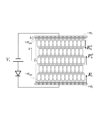
The spontaneous polarization of a photoferroelectric usually decreases Ikeda, Sasaki, and Ichimura (1993); Langhoff and Giesselmann (2002); Saipa et al. (2006) under light irradiation as photons are absorbed and modify the polar ordering. Since light is absorbed the beam is necessarily attenuated and the polarization profile can no longer be uniform (except when light is powerful enough that at all depths ). Then is non-zero also in the bulk, and polarization charges will emerge inside the sample as well as at the surface. Consequently a non-uniform electric field appears in the sample, where is the electric polarization at the point and the illumination time ; note that . As the diode prevents backflow of the charge to the battery (see Fig. 1), the resulting voltage between the electrodes will be greater than :
| (2) |
where the distance is measured from the center of the sample (Fig. 1). Writing for the spatial average of the polarization profile after time , and replacing with the aid of Eqn. (1), we get
| (3) |
The described mechanism can be exploited to pump charge from a low to high voltage battery. Many different materials exhibit photoferroelectric behavior, and might be potential candidates for use in our device. We therefore explore the suitability of these materials for a charge pump, optimize their performance by specifying an appropriate electric circuit, and calculate the efficiency of such pumps. Our general analysis is applicable to all photoferroelectric materials. Only our final estimate of the efficiency of the pump will be demonstrated for particular substances, photoferroelectric liquid crystals.
The circuit diagram of the charge pump is shown in Fig. 2. The central component of this circuit is the photoferroelectric sample S placed between transparent conducting electrodes. The arrangement of diodes is such that the charge can flow from the voltage to a higher voltage only. We shall describe how the electric polarization varies during a cycle.
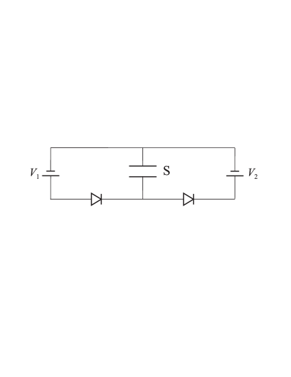
The photoferroelectric sample S in the dark state is connected to the voltage . When light is shone on the sample, the electric polarization decreases and the voltage across the electrodes is increased above the value , with charge on the electrodes being fixed (the left diode prevents backflow of charge). As the electric polarization further decreases, the voltage across the electrodes increases until it reaches the value . Then the charge starts to flow through the right diode, which leads to its being pumped into battery at constant voltage (Fig. 2). If the connection of the sample with the battery were absent, the voltage across the sample would rise to a value we simply denote by corresponding to with , the duration of the illumination phase of the cycle.
The charge transferred to the battery is equal to , where is the total capacitance of the sample. There are two insulating layers of capacitance and a liquid crystal of capacitance connected in series. The equivalent capacitance is given by , where is the area of the electrode. Taking into account that , and typically , one gets a simple expression .
Upon switching off the light, the spontaneous polarization will evolve to a new state. Here, we shall suppose that it recovers its initial dark state value; this, in particular, holds for a large class of photoferroelectric liquid crystals. As the polarization increases in time, for a constant value of the charge on the electrodes, the voltage across the sample starts to decrease from its value . When the voltage drops to , new charges will start to flow from the left battery to maintain the voltage across the electrodes. Finally, the charge on the electrodes recovers its value at the beginning of the cycle. This cycle is reminiscent of an optical charge pump based on a capacitance that is optically variable. Hiscock, Warner, and Palffy-Muhoray (2011) In practice, a self-priming circuit McKay et al. (2010) would avoid exhausting battery .
The same total charge pumped into the battery is supplied by to the electrodes during recovery process. Thus, the work output of this charge pump is , which gives
| (4) |
We can maximize this output with respect to the voltage difference . Using the condition , we get the optimal choice of voltage difference
| (5) |
Since to pump charge we require the open circuit developed voltage to exceed that of the upper battery, that is , or equivalently , we see that the above choice of voltage difference is allowed. Thus, for given voltages and , the optimal is
| (6) |
The maximum output is then
| (7) |
Output is therefore higher if the dark state polarization and the average value of the polarization profile in the illuminated state differ more, that is if as much polarization as possible is lost. The work delivered depends on the volume of the working material.
If is the incident solar flux, and is the energy input per unit volume of the sample required to transform the polarization state of the working material, then is determined by energy balance . The period of a cycle then follows. Here, is the characteristic time for relaxation of polarization to its dark state value. The power efficiency is then .
The power efficiency of this cycle is significantly reduced, due to the fact that no work is done during the time . To avoid such kind of difficulties one can use an array of photoferroelectric samples. They could be sequentially illuminated and then allowed to relax back to the dark state, either via a movable focusing mirror, or by rotating an array of samples. It is clear, however, that the described setting will reduce to some extent the desired enhancement of power efficiency. As typically , one should use an array of at least samples. For such a device the power efficiency is given by the above formula, but in which the cycle time is equal to , that is
| (8) |
To obtain a numerical estimate of the power efficiency (8) we confine ourselves to photoferroelectric liquid crystals, the main properties of which we sketch.
Liquid crystals are anisotropic fluids which usually consist of rod-like molecules. The liquid-crystalline states are observed at temperatures between the solid state and the ordinary isotropic liquid state. In the simplest nematic phase long-range translational order is absent, but the long molecular axes are orientationally ordered, on average about a unit axial vector , the director. In addition to nematic orientational order, the molecules in smectic phases are arranged into layers. In the smectic A phase (SmA), the molecules are organized as two-dimensional anisotropic liquids within the layers, with the nematic director being parallel to the normal of the layers. In the smectic C phase (SmC), is no longer parallel to , but is tilted by an angle with respect to (Fig. 3). The tilt angle is a function of temperature . At a given , the director is located on the surface of a cone centered around with opening angle .
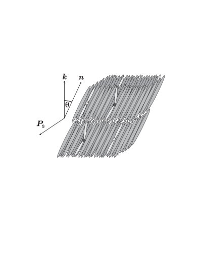
A SmC liquid crystal composed of chiral molecules is referred to as a SmC* (Fig. 3). As first pointed out by Meyer Meyer et al. (1975), the emergence of a (local) spontaneous electric polarization in SmC* is allowed along since the plane of and is not a mirror plane. The spontaneous polarization is a function of the tilt angle, Lagerwall (1999) and for small . When the temperature is increased and crosses a threshold value, the SmC* phase most often undergoes a second-order phase transition to the non-polar SmA* phase.
The spontaneous polarization of a SmC* phase doped with photosensitive molecules (for example, an azo or thioindigo dye) can be changed by light irradiation; Ikeda, Sasaki, and Ichimura (1993); Langhoff and Giesselmann (2002) pure systems of dyes have also been used. Saipa et al. (2006) Some dye molecules can make transitions from the linear (trans) ground state to the excited bent-shaped (cis) state by absorbing a photon. The cis state isomers can disrupt the SmC* ordering, which leads to a change of , whence the name photoferroelectric effect. If the interaction with light is sufficiently strong it can completely destroy the SmC* phase, causing a transition to the non-polar SmA* phase. Dye molecules in the excited cis state re-isomerize thermally back to the ground trans state with some characteristic time. Upon removal of light, the electric polarization eventually regains its initial dark state value. Recently, it has been argued that the mechanism and details of light absorption are crucial to understanding the optical depression of electric polarization. Knežević and Warner (2012) In particular, it has been shown that the spontaneous polarization displays a non-uniform profile through the sample.
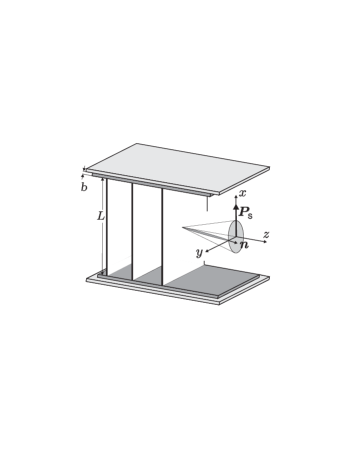
Here we suppose that the sample is confined between two parallel plates so that the smectic layers are perpendicular to the plates – the bookshelf geometry (Fig. 4). The smectic layers usually shrink to some extent at the tilting transition from the paraelectric SmA* to polar SmC* phase and form a folded chevron structure. Rieker et al. (1987) Given that materials without substantial layer shrinkage de Vries, Ekachai, and Spielberg (1979) have also been found, in our simple analysis we shall neglect this shrinkage. Charge pumps made of samples with large electric polarization in the direction perpendicular to the electrodes have larger efficiency. A perpendicular polarization can be achieved by applying a voltage between the electrodes. Indeed, a simple extension of the approach of reference [Čopič, Maclennan, and Clark, 2002] reveals that for voltages higher than the sample’s polarization is perpendicular to the electrodes. For , , and for a SmC* material with we get a small voltage . We see that the polarization will have the required direction provided that the voltage (Fig. 2) is greater than .
Typically one deals with SmC* hosts doped with dye molecules, whose number fraction is a few percent. The behavior of the average polarization after time can be described theoretically. Knežević and Warner (2012) Here we shall simply suppose that the light is sufficiently intense so that there is a time () such that vanishes. In other words, we can regard as the minimal time needed for a sufficient depletion of the trans dye population to eliminate the polarization. Taking , formula (3) for the voltage reduces to . For instance for a SmC* material with and in a cell of thickness one obtains a , which is much larger than . Therefore, the optimal voltage is .
Supposing that , the efficiency (8) is
| (9) |
Provided that is shorter than the characteristic time of thermal recovery of spontaneous polarization, and the process of back photoconversion from the cis to the trans state of dye molecules can be neglected, the input energy can be expressed as . Here is the number of trans dye molecules per unit volume that need to be converted to cis to eliminate , and is the energy each dye molecule absorbs from the light beam.
To get a numerical estimate of the efficiency we take as an example a polar SmC* host W314 doped with a few mol of a racemic mixture of W470 azo dyes Walba et al. (1991); Lanham (1999); *chang:00 (higher dye loadings lead to lower conversion due to flux attenuation Saipa et al. (2006); Knežević and Warner (2012)). These two compounds have a very similar structure, the N=N double bond of W470 being the only difference. The polarization of the W314 host at is roughly and is one of the highest outside bent-core molecules. Niori et al. (1996) The trans absorption maximum of W470 dyes is located at , which corresponds to photons of . We assume that the quantum efficiency for the trans to cis transition is equal to . The relative molecular mass of W314 is , and assuming a density of roughly , we obtain a total molecular number density . If only, say, of molecules need to be converted to cis to eliminate the polarization, we obtain . Taking the dielectric constant of W314 in the direction perpendicular to the director (see Fig. 4) as , the efficiency (9) is . Multiple layers with different dyes which absorb photons of different energies would capture more of the broad solar spectrum. A gradient of dye species can be stabilized by bonding them into an elastomeric SmC* host – a loosely linked solid that is still able to change its degree of order. Such solids also reduce the risk of charge transport under fields ( here) as in dielectric actuation using rubber. McKay et al. (2010) Lower energy photons would give correspondingly higher efficiencies .
Let us briefly consider the case of a non-zero polarization profile through the sample. We adopt a simple model for this profile, namely, we assume that the polarization is eliminated in a layer of thickness , while in the rest of the sample it is uniform and equal to the dark state polarization . Then we can write . As can be roughly estimated as , for the power efficiency we get . The efficiency is, therefore, reduced by a factor of with respect to (9).
Our pump could equally work on cycles of temperature change that change the spontaneous polarization. In this case the input energy is , where is the specific heat per molecule at temperature , and the integral goes from the dark state temperature of ferroelectric material to the temperature where the spontaneous polarization is eliminated (SmC*-SmA* phase transition temperature for liquid crystals). The heat that is unavoidably generated by optical absorption thus adds to the efficiency of our optical energy harvester.
In summary, we have proposed a light-powered charge pump for energy conversion, using a photoferroelectric working material. The efficiency is explicitly given, which makes clear directions for further increase.
M.K. thanks the Winton Programme for the Physics of Sustainability and the Cambridge Overseas Trust for financial support, and M.W. thanks the Engineering and Physical Sciences Research Council (UK) for a Senior Fellowship. The authors thank David Walba for advice.
References
- Ikeda, Sasaki, and Ichimura (1993) T. Ikeda, T. Sasaki, and K. Ichimura, Nature 361, 428 (1993).
- Langhoff and Giesselmann (2002) A. Langhoff and F. Giesselmann, J. Chem. Phys. 117, 2232 (2002).
- Saipa et al. (2006) A. Saipa, M. A. Osipov, K. W. Lanham, C. H. Chang, D. M. Walba, and F. Giesselmann, J. Mater. Chem. 16, 4170 (2006).
- Hiscock, Warner, and Palffy-Muhoray (2011) T. Hiscock, M. Warner, and P. Palffy-Muhoray, J. Appl. Phys. 109, 104506 (2011).
- McKay et al. (2010) T. G. McKay, B. O’Brien, E. Calius, and I. Anderson, Smart Mater. Struct. 19, 055025 (2010).
- Meyer et al. (1975) R. B. Meyer, L. Leibert, L. Strzelecki, and P. Keller, J. Phys. (Paris) Lett. 36, L69 (1975).
- Lagerwall (1999) S. T. Lagerwall, Ferroelectric and antiferroelectric liquid crystals (Wiley-VCH, New Jersey, 1999).
- Knežević and Warner (2012) M. Knežević and M. Warner, J. Chem. Phys. 137, 144902 (2012).
- Rieker et al. (1987) T. P. Rieker, N. A. Clark, G. S. Smith, D. S. Parmar, E. B. Sirota, and C. R. Safinya, Phys. Rev. Lett. 59, 2658 (1987).
- de Vries, Ekachai, and Spielberg (1979) A. de Vries, A. Ekachai, and N. Spielberg, Mol. Cryst. Liq. Cryst. Lett. 49, 143 (1979).
- Čopič, Maclennan, and Clark (2002) M. Čopič, J. E. Maclennan, and N. A. Clark, Phys. Rev. E 65, 021708 (2002).
- Walba et al. (1991) D. M. Walba, M. B. Ros, N. A. Clark, R. Shao, K. M. Johnson, M. G. Robinson, J. Y. Liu, and D. Doroski, Mol. Cryst. Liq. Cryst. 198, 51 (1991).
- Lanham (1999) K. W. Lanham, Master’s thesis, University of Colorado, Boulder (1999).
- Chang (2000) C. H. Chang, Master’s thesis, University of Colorado, Boulder (2000).
- Niori et al. (1996) T. Niori, J. Sekine, J. Watanabe, T. Furukawa, and H. Takezoe, J. Mater. Chem. 6, 1231 (1996).