Stroboscopic wave packet description of time-dependent currents through ring-shaped nanostructures
Abstract
We present an implementation of a new method for explicit simulations of time-dependent electric currents through nanojunctions. The method is based on unitary propagation of stroboscopic wave packet states and is designed to treat open systems with fluctuating number of electrons while preserving full quantum coherence throughout the whole infinite system. We demonstrate the performance of the method on a model system consisting of a ring-shaped nanojunction with two semi-infinite tight-binding leads. Time-dependent electron current responses to abrupt bias turn-on or gate potential switching are computed for several ring configurations and ring-leads coupling parameters. The found current-carrying stationary states agree well with the predictions of the Landauer formula. As examples of genuinely time-dependent process we explore the presence of circulating currents in the rings in transient regimes and the effect of a time-dependent gate potential.
PACS numbers: 73.63.Rt
1 Introduction
Transition from the state with zero electric current to a state with nonzero current in nanoelectronic devices is a technologically important example of non-equilibrium quantum dynamics of an open many-electron system. It exhibits several significantly different time scales related to relaxation of electrons with important consequences for the prospects of their applications in nanoelectronics. The common problem in theoretical quantum transport description in both stationary and time-dependent situations is proper inclusion of the semi-infinite leads. The number of degrees of freedom in the nanojunction, which are explicitly considered, has to be sufficiently small in order to be numerically tractable. Hence the boundary conditions at the junction must be correctly described and included. An approach widely used for stationary systems are the non-equilibrium Green’s functions (NEGF) with lead self-energies [1, 2] which include the physics induced by the leads.
The description of boundary conditions of the finite nanojunction becomes more complicated in time-dependent problems. The non-stationary quantum transport has been addressed for non-interacting electrons [3], within the time-dependent density-functional theory (TDDFT) [4, 5] or even the many-body perturbation theory [6]. It has been shown that self-energies – now time-dependent – could in principle be used also in this case as long as the leads are treated at the TDDFT level. In practice, it is a quite complicated approach especially for realistically structured systems so that simplifications of the formalism are necessary [7, 8]. Chen et al. proved the so-called holographic electron density theorem and developed a new method for time-dependent open electronic systems [9]. Further effort in this direction led to computationally more efficient density-functional tight-binding method [8]. Very recent works of Chen et al. on time-dependent quantum transport are based on Liouville-von-Neumann equation for single-electron density matrix [10]. Another recent work by a different group [11] uses generalised master equation approach to mesoscopic time-dependent transport. Non-equilibrium thermodynamical theory of interacting tunnelling transport has been presented by Hyldgaard [12].
Another class of methods to tackle time-dependent transport with open boundary conditions has been in development [13, 14, 15]. The scope of these methods is wider than just elastic transport. The methods are know as correlated electron-ion dynamics (CEID). The dynamics is based on Ehrenfest molecular dynamics and its extensions. The electronic degrees of freedom in CEID are divided between the central system and its environment which is facilitated by the formalism of one-particle density matrices. A damping term has been introduced used in the open-boundary equations of motion [13]; this term keeps the environment close to a reference state. In further development of the method [14], open boundaries have been introduced in a new way which represents an explicit realisation of an external battery. We remark that this method does not conserve coherence between injection and subsequent scattering of the electrons.
In the present work we address the open-boundaries time-dependent quantum transport problem using the stroboscopic wave packet (SWP) basis method, principles of which has been provided in the works [16, 17]. We study time-dependent currents through model-system nanojunctions formed by small rings inserted to electric circuit formed by mono-atomic leads. We also present new developments of the stroboscopic wave packet approach (SWPA) which are necessary in order to describe the systems with atomistic structure. While in the orginal works [16, 17] structureless electrodes and very simple tunnelling barriers have been used to demonstrate the method, here we work with atomistic models of the electrodes and more complex nanojunctions. The formulation presented here solves the time-dependent Schrödinger equation (SchE) for independent electrons within the tight-binding (TB) approximation. SchE is solved numerically with state vectors expanded in the stroboscopic wave packet basis representation (SWB) [16, 17]. The SWPA has been designed to be specifically suited for time-dependent transport through nanojunctions. Its main advantage is to make possible explicit integration of equations of motions of nanojunction degrees of freedom with full quantum coherence preserved throughout the whole infinite system. This can be viewed also as an open-system treatment with correct inclusion of boundary conditions. In the present paper we focus our study on simple model cases of rings and monoatomic leads with possible extension to realistic systems. Our main interest are transient currents developed in response to abruptly applied bias and time-dependent gate potential. We also refer to stationary results obtained by other authors using analytical methods.
Transport properties of atomic-scale sized rings have been studied by several authors in most cases on the Hückel/tight-binding level of description and in the stationary regime. Effect of the asymmetric position of lead on transmittance has been studied in Ref. [18] by means of Green’s functions. Authors of work [19] have developed a source-sink potential method for convenient analytical treatment of molecular electronic devices including conjugated systems. This approach has been used in Ref. [20] to obtain the form of the transmission with explicitly given dependence on the molecular skeleton and its connection to leads. Authors of Ref. [21] generalised the so-called waveguide approach [22] (WGA) to systems described by the TB approximation. Resulting methodology – the tight-binding waveguide approach (TBWGA) – can be interpreted as a route to an exact solution of the stationary SchE for given class of TB models. An explicit formula for transmittance has been derived [21] for rings composed of identical atoms and identical nearest-neighbour couplings and coupled to two leads with equal chemical potentials in both of them. The authors discussed conditions for occurrence of circulating currents in such quantum rings. More recently Sparks et al. formulated the stationary problem more generally, considering a multibranch device in a TB approximation [23]. They provided an explicit formula for system transmittance valid for a large class of systems including those with different chemical potentials in different leads. The formula has been obtained by an exact solution of the stationary SchE for the whole system and has also been related to Green’s function analysis. Explicit results in Ref. [23] facilitate the study of quantum interference effects in stationary regime for wide class of systems. We refer to these results especially when the long-time behaviour of our time-dependent method is discussed. An inspiring computational work was done by Saha et al. [24]. The authors study a true atomistic model of a quantum-interference-controlled molecular transistor formed by an 18-annulene attached between zigzag graphene nanoribbons. The device was studied by a multi-terminal NEGF-DFT formalism [25] and the current-switching effect was confirmed.
On the experimental side, ring-shaped tunnel nanojunctions can be formed by cyclic organic molecules attached between two electrodes (see for example [26, 27, 28, 29]). Conductors can be formed by metallic (usually Au or Pt) electrodes or by graphene nanoribbons [30, 31]. These works employ direct attachment of particular molecules in between metallic electrodes (Pt-C or Au-C bonds) using mechanically controllable break junctions. Such contacts are reported to be more conductive and stable than previously more common junctions employing a bridging thiol group (thus forming a metal-S-C bond) [32]. Another realisation of nanometer-scale sized rings is fabrication of structures on proper substrates [33, 34, 35]. This can be done using molecular-beam epitaxy, wet etching and optical or electron-beam lithography. Finally we note that the concept of a quantum interference driven transistor started to be more explicitly discussed in literature relatively recently [36]. It still represents an experimental challenge and a major bunch of experimental results is yet expected to come.
The paper is organised as follows. In Sec. 2 we describe the model of the atomic ring. In Sec. 3 we explain the implementation of the stroboscopic wavepacket method. In Sec. 4 we provide the formula which we implement for electron current calculations. Sec. 5 describes stationary results as a basis from which we move into non-stationary regime in section 6, which contains our main results.
2 The model of the ring with contacts
We consider a linear chain of atoms, each two being a lattice constant apart, with one finite ring which presents an obstacle for the flow of electrons (Fig. 1). All couplings are considered within the TB approximation in which we limit our treatment to one orbital per atom The chain is periodic apart from the ring region. Hence, the TB Hamiltonian is of the form
| (1) |
where
| (2) |
and are the fermionic creation and destruction operators, is a constant on-site energy in the chain, and is the TB hopping parameter here assumed to be negative. The important simplifying assumption is that there is only one localised atomic orbital (state ) per each site. The represents the unperturbed chain, later referred to as the lead’s Hamiltonian.
is a stationary, periodicity-breaking term. Its form corresponds to a TB ring structure, indicated in Fig. 1. (Specified values of and are taken only as an example there.)

In the simplest case, the modifications to the periodic chain Hamiltonian due to the ring presence will be expressed by the following matrix elements of :
| (3) |
All other matrix elements of are zeros.
Applied bias will be modelled by time-dependent shifts of the on-site energies. If a bias voltage is applied then the on-site energies of the left lead will take values , being magnitude of electron charge. The operator expressed in the atomic-orbital basis has the following matrix elements:
| (4) |
The on-site energies within the ring, if not differently specified, will thus take values . The on-site energies in the right lead will remain unchanged, equal to the equilibrium value .
Three exceptions from the above prescription of the perturbation are studied: (i) In Sec. 6.1.2, where a uniform slope of the potential energy within the ring is used instead of the spatially constant value , (ii) in Sec. 6.3, where a time- and branch- dependent gate potential is is used, (iii) finally consideration of variable coupling strength between the ring and the leads in Sec. 6.4.
3 The stroboscopic basis set
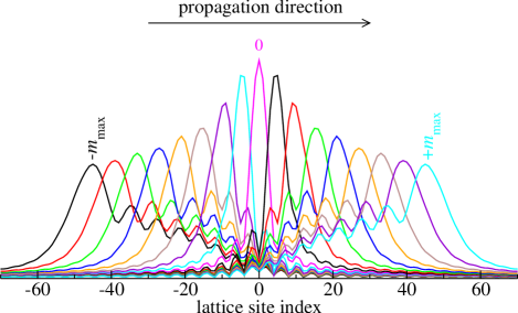
The stroboscopic wavepacket basis set consists of wavepackets (Fig. 2) constructed from the eigenstates of the unperturbed (lead’s) Hamiltonian (2). The mathematical expression for the basis set vectors is [16, 17]
| (5) |
where is the lead’s Hamiltonian and are its eigenstates normalised so that . Each basis function or wavepacket (5) is uniquely characterised by three indexes: the band index , the time shift index , the degeneracy index and time .
The band index . The unperturbed Hamiltonian (2) gives the dispersion relation
| (6) |
The corresponding energy range is in the SWPA divided into non-overlapping bands [16]. band has its energies . In our present work we use two equally wide bands () [37] spanning the whole TB energy range. The band index then takes values 1 a 2.
The time-shift index . Within each band, different, mutually orthogonal basis functions are obtained by time shifts , where the time step
| (7) |
is set by the energy width of the band . attains all integer values, but in numerical calculations it is restricted to , as it is discussed at the end of this section.
The degeneracy index . Apart from the energy, each eigenstate of the lead’s Hamiltonian has further quantum numbers. In the present system, the only one is the direction of propagation of the Bloch eigenstates: those propagating from the left to the right (index ) and the opposite ones (index ).
The time . The time in the notation indicates that the basis state is unitarily propagated [17] by the lead’s Hamiltonian (2). The use of this “moving” basis set significantly simplifies the form of the SchE in the SWB representations (see Eq. 11 below), very much in the spirit of using the interaction representation in formal perturbation theory in quantum theory. At each given time the SWB vectors form an orthonormal system since
| (8) |
The set of basis states (5) is complete if is infinite.
Given the form of Hamiltonian (1), each electron in the system evolves independently as described by the SchE
| (9) |
State vectors for each electron are expanded in this basis set:
| (10) |
where we have introduced a composite index . The SchE provides a linear system of differential equations for each of the involved electrons. Due to the time-evolution of the basis functions given by the operator , the equations for amplitudes include matrix elements of the perturbation only:
| (11) |
with . This is of key importance for our method: basis set wavepackets, which are localised far from the central region feel either zero perturbation (in the right lead, and hence their matrix elements are zeros) or they feel only the spatially uniform bias-induced potential of the left lead; see eq. (4). For such matrix elements we have
| (12) | ||||
| in the left lead, for packets far from the central region |
meaning that probability amplitudes of the wavepackets evolve freely, (independently of other amplitudes) far in the left lead. Situation is even simpler far in the right lead where is zero and corresponding amplitudes do not evolve at all. The constant or freely evolving amplitudes need not be explicitly included into simulation and this omission in principle does not have any impact on accuracy of the simulation. In practice, since the SWPs are not strictly localised, by using the finite cutoff we introduce certain error into simulations.
The simple form of equations of motion (11) has been possible due to the employment of the moving (i.e. unitarily propagating) basis set. The simplicity is in that the matrix elements are computed only from the interaction term of the total Hamiltonian (1).
Wavepackets corresponding to vectors (5) unitarily propagate in time which implies that each particular packet will travel away from the central region after some time. The result would be that (for finite ) at large times the region would not be covered by basis set wave packets at all and no electrons would be presents in the central region at long times. In detail, the unitary propagation of the wavepackets is such that during a time interval [defined below (5)] each packet moves exactly to the position of the neighbouring packet (either on its left or on its right, depending on the propagation direction). If we had a very large basis set () and were looking at a movie of the wavepackets only at the “stroboscopic” times , we could not see any motion of the packets. For any finite we could observe similar static picture only for a limited time and in a limited spatial region because the wavepackets constantly propagate from one’s position to the other’s.
To prevent the gradual disappearance of the basis functions from the central region in simulations, we periodically insert new basis wave packets into the system at every period . The newly inserted packets are localised far away from the centre, but moving toward it. To avoid the increase of the total number of basis vectors, we also periodically remove basis wave packets (those which has left the central region). In other words, we remove the leading wave packet from the train of the propagating packets and attach a new wave packet at the tail of the train. (See also Fig. 2.) This removal/insertion procedure is accomplished for each band (indexed by ) independently; different bands could in principle have different widths and consequently different parameters . For given band there are two such procedures: one for (packets propagating from right to left), the other for (packets propagating from left to right). In this way we keep the basis set vectors in the region of interest (the “central region”) and also keep the number of the vectors constant.
It is necessary to have sufficiently large so that the basis vectors with are decoupled from other basis vectors (see more reasoning below) and hence the removal of the basis vector does not affect the quantum dynamics of the electron, amplitude of which has been removed.
In addition to the basis vector removal/insertion procedure, we also track individual electrons in the simulation. Each newly inserted basis state, if belonging to normally occupied band ( in this work), is set to be occupied at the instance of the insertion. Also, an electron, which through time evolution gets far from the central region, is removed from the simulation according to a proper criterion. Therefore the simulation explicitly describes an open system in which the total number of electrons generally fluctuates [38].
The initial conditions applied to the probability amplitudes are such that
| (13) |
i.e. only the lower band is initially occupied.
Matrix elements of are evaluated using the overlaps . In Appendix we derive that the overlaps can be expressed by the formula
| (14) |
Quantities are dimensionless wavenumbers corresponding to energies through the TB dispersion relation (6). The cutoff on atomic sites indexed by has to be chosen sufficiently large in order to cover all SWPs (5) included into simulation. For majority of calculations we use with rather conservatively chosen . In one case we use and corresponding . Integrals in (14) have to be evaluated numerically.
The SWPA as described above and used in this work does not include any electron-electron (e-e) interactions except for keeping them always in strictly orthogonal states. We expect that e-e interactions with effects like Coulomb blockade among others become more important for weakly coupled rings (although they can never be neglected in any accurate quantitative description) [39]. Further developments of the SWPA will include also realistic e-e interactions at least on a mean-field level of description like in time-dependent Hartree-Fock theory or in TDDFT. Presently we could only include a simple dynamical mean-field interaction according to a chosen model. Having done this we have not found any significant interesting impacts of the interaction. Hence we decided not to include any such results in the present work as it would present an unnecessary complication.
The system of the equations (11) is solved using the modified-midpoint method [40]. Its accuracy and stability is fully sufficient for given problem. As a complementary treatment applicable for stationary currents, we compute exact stationary currents for given TB Hamiltonian (1) in cases when it is time-independent. See Sec. 5 for more details.
4 Electron current formula
In this section we briefly provide an expression for local electron current. For this purpose we consider one-dimensional infinite TB chain, specified in Sec. 2. For such a system the local current operator at bond between sites and is given by the formula (see Ref. [1], p. 162 therein).
| (15) | |||
being the spin index. Taking the expectation value in a single-electron state we obtain
| (16) |
Superscript marks that it is a current caused by single electron; we must sum up over all electrons in the system to obtain the total current. If we express the state vector in the stroboscopic basis orbitals then we obtain
| (17) |
The factor of 2 has been added to take into account two electrons differing only by their spins. As for the sign convention used for the current expressed by eqs. (16), (17), it indicates flow of particles (electrons), not the charge. The same purely local result for as shown above could be derived also for currents in particular ring arms. Hence we use formula (17) to compute time-dependent current (contribution from one electron) through any chain (lead or arm of the ring) of the complete system. The total current is obtained by summing up contributions (17) generated by all individual explicitly included electrons in the system:
| (18) |
5 Stationary currents through ring nanojunctions
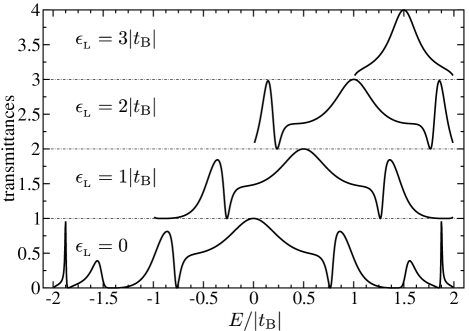
Currents through TB rings have been studied in literature mostly in stationary regimes. It is convenient to compare quasi-stationary currents from our method to exact stationary results for the TB model. For this purpose, the whole system – ring with leads – is assumed to be composed of identical atoms described by the simple TB Hamiltonian with all couplings equal to . The only perturbation to periodic chain Hamiltonian are then terms (3) which represent a perturbation to the topology of the linear chain. It was shown in Ref. [21] that in the stationary regime there are both conducting and insulating configurations depending on where the leads are attached to the ring. Specifically, all odd-numbered rings are always conductive irrespective of the choice of attachment site. On the other hand, even-numbered rings can exhibit both behaviours. These findings are confirmed and extended by the exact TB results of Ref. [23].
We have obtained stationary results from exact eigenstates of the TB Hamiltonian defined in Sec. 2. This approach is, for the Hamiltonian used in our work, equivalent to the method described in Ref. [23]. As specified in Sec. 2, the applied bias is modelled by lifting on-site energies in the left (source) lead at the value . The on-site energies in the right lead (drain) are kept at . On-site energies of all ring atoms are kept at the intermediate value . TB couplings are unchanged, i.e. they all are equal to . The eigenstates for such system are expressed in the TB basis,
| (19) |
They depend on the eigenenergy and the direction of propagation . For brevity we do not show these dependences explicitly. We compactly represent the amplitudes by composite formula
| (20) |
with
| (21) |
The specific form of (20) is an abbreviated non-standard notation mimicking the spatial positions of particular system chains and has to be understood in the sense that for left lead, for lower ring branch, etc. We introduced the dimensionless k-number
| (22) |
with being the lattice constant. is the local density of states (DOS) of an ideal infinite chain for a particular branch of the system and for the TB model is expressed as
| (23) |
, identified with , or , is the value of the on-site energies in given branch of the system. In the model under study it also represents Fermi energies of particular bulk systems. Indices L, S and R stand for the left lead, small system (the ring) and the right lead, respectively [41].
When convenient we use also notations , and to distinguish DOSs in the left lead, right lead and in the small system (ring). Parameters and describe wavefunction of the left lead, parameter in the right lead, and in the lower ring arm and finally and in the upper ring arm.
An electron being in particular eigenstate is then interpreted as partially reflected and partially transmitted, with transmittance computed as
| (24) |
This simple formula is applicable also in cases when the Fermi levels in the two leads are different. In such a case we need additional factors involving the respective group velocities. These factors have been explicitly inserted into functions (21) hence are not explicitly present in the formula (24). The results from exact eigenstates for the ring of sites and are shown on Fig. 3.
Having transmittances available, we compute the stationary electron currents in the leads using the Landauer formula
| (25) |
We remind that the transmittance depends parametrically also on the chemical potentials in the leads (which are equal to and ) and on the on-site energies of the ring atoms which are all equal to . In the eigenstate approach we always use and (applied bias) and the on-site energies of the ring are set to .
The integral in Eq. (25) is done numerically. In Fig. 4 we show the comparison of the exact stationary currents and the currents obtained by the time-dependent wavepacket approach.
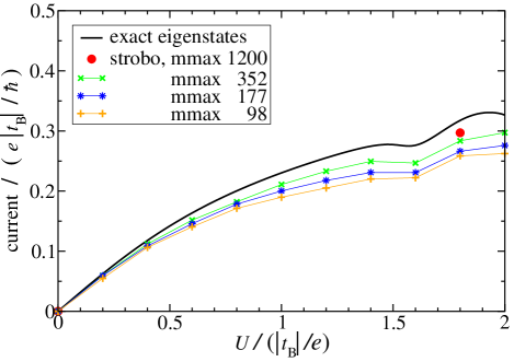
Results from the SWPA (discrete symbols) represent long-time quasi-stationary values from time-dependent calculations. We see overall agreement between the two approaches, especially for low biases. The results from eigenstates are exact for given Hamiltonian. The SWPA [16, 17] is in principle exact too, but its accuracy is lowered by the finite cutoff to the number of basis functions which is . The impact of the finite cutoff is typically not important at low biases but increases with the bias and the obtained accuracy is then lower at high bias conditions. Convergence of the current with the cutoff becomes very slow at large . Several examples computed with different basis set sizes are shown on Fig. 4. The steady-state current in the leads is always underestimated [42] when finite is used. To understand the finite basis set impact, we first remark that the dynamics of an individual electron becomes (quite obviously) more accurately described when using larger , hence providing more accurate current (17) generated by single electron. Second, the increased results in a larger number of electrons included into the total current formula (18). As a consequence, the precise dependence of the current on is a complicated function. The much slower convergence at higher values of can qualitatively be understood as a result of larger spread of the SWPs at hight (shown on Fig. 2). In the limit of the packets become fully delocalised. Individual high- packets contribute very weakly to the total local current at given point in space. The less converged results in absolute terms are pronounced especially at larger biases. The convergence is worse also in relative terms: at we reach of the exact limit (Fig. 4). At we get and at only , all at . The worse convergence at larger biases can be qualitatively understood on the basis of the equations of motion (11) and bias-related matrix elements (12). Using a finite in (11) we drop some portion of the exact equations of motion, in particular some of the terms (12) which describe the interaction with bias-induced lifts of on-site energies in the left lead. Using higher bias increases significance of those matrix elements and hence makes convergence more difficult. The finite basis set size would not impact the accuracy of our approach if the stroboscopic basis states with large indices were well localised in space. In reality, even wavepackets with very large indices exhibit long tails towards the central point of the lattice where the nanojunction is placed. Ideally, having basis wavepackets (those with large indices) with no tails in the nanojunction region would result in perfectly converged results. (Such an ideal situation is impossible because of the dispersion which spreads the wavepackets. Our further effort in development of the SWPA is directed to overcome the convergence issues despite the presence of the dispersion.)
6 Simulations
6.1 Bias voltage switch on ring-shaped nanojunction
Time-dependent bias is modelled by given time-dependent (but spatially uniform) lift of the TB on-site energies in the left lead only. The atoms in the right lead have their on-site energies all set to zero, which is also the value of Fermi energy in equilibrium.
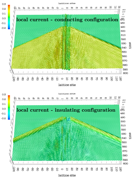
The atoms within the ring have their on-site energies set to the half of the bias value applied at given time although we test also different model in subsection 6.1.2. In our simulations we first “equilibrate” given system by letting it evolve at zero bias (and zero temperature) for time up to . The “equilibration” evolves the non-interacting many-electron initial state of the system, described by eq. (13), into (again non-interacting) stationary many-electron state of the Hamiltonian with the localised perturbation (the ring system and eventual variations of some of the on-site energies or interatomic couplings). We have verified that the equilibration period is sufficient to obtain converged transient electric currents in the sense that these currents are practically independent of particular choice of if is at least . The transient electron currents are evaluated according to formula (17), with applied summation over all contributing electrons in the system. We study how these transient currents depend on several ring parameters like the ring size, placement of the terminals and the magnitude of applied bias. Typical behaviour of the transient electron currents is shown in Fig. 5. It is noticeable that both the temporal and spatial evolution must be considered. The intersect of the two ridges corresponds to the time when the bias was turned on and to the spatial location of the ring. The slope of the ridge corresponds to the Fermi velocity, , so that the time interval between the instance of switching-on the bias and the arrival of the density or current perturbation to a site is given by the expression . The ridge on the left side corresponds to the reflected electron impulse propagating back into the left lead. Similarly, the other ridge represents the transmitted wavefront in the right lead. The function values are mostly positive meaning that the currents in both leads are positive (i.e. electrons flow from the source lead to the drain lead). Results for several specific cases are discussed in the following subsections. Presented ring sizes vary from 16 to 18. We have calculated also several other sizes, starting from , not shown here. Plotted local currents will typically correspond to a lattice site positioned far from the ring, in most cases site , which is displaced about 100 lattice constants from the considered rings.
6.1.1 Dependence on the location of drain vertex
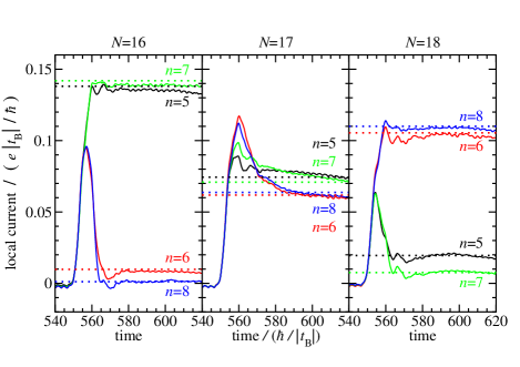
The dependence of the time-dependent current on the position of the right (drain) lead is shown in Fig. 6. We show how and if the transient currents (induced by the abrupt bias switch at time ) depend on chosen drain vertex site . In Fig. 6 we plot transient local currents obtained from our simulations for three subsequent rings sizes and several drain-lead attachments. These rings represent various different kinds of electronic transport properties which can be found in rings. The local currents shown have been calculated at lattice site 120. The finite basis set adds rapid oscillations on the computed local currents111The period of these artificial oscillations is always , the quantity defined by eq. (7), here equal to (same for both the bands). The oscillations are larger at sites closer to the ring. All this is explained by the localised nature of the stroboscopic basis states (the wavepackets) and the finite number of them. The train of the wavepackets (see Fig. 2) travels in real space in such a way that during a time interval each packet places itself exactly to the position which was occupied by its neighbour at time . Since we use the finite cutoff on the basis set, the quality of the description at given point of space fluctuates in time with the period of . Instead of using a huge value of (which would be prohibitively expensive) we smooth out the oscillations by averaging them over the time interval of about . Typical timescales of the processes studied in the present work are in most cases much larger than and the relevant effects are not affected by the oscillations or by their artificial smoothening.. We smooth out the oscillations by averaging them over the time interval of about . This averaging does not modify essential features of the plots including the characteristic times and rates. Example of the raw unaveraged data are shown in Fig. 7. The “no slope” black curves in that figure are obtained in the same system as plots and in Fig. 6, apart from the time averaging.
The onset of the electronic responses appears at times around , which is delayed about 50 time units after , caused by the distance from the ring to the observation site []. We see, that similarly as in the stationary regime, the time-dependent simulations also exhibit the two very different regimes - the conducting and insulating one. However there is the peak of transient current even in the insulating configurations after the bias is switched on. This feature is shown in the lower panel of Fig. 5 and will be discussed also below.
rings. The left panel of Fig. 6 shows results for rings of size , but differing by the position of the drain vertex sites which run through the sequence . The odd-numbered cases ( and ) correspond to conducting configurations. The well conducting state of the ring is given by constructive interference (CI) of the electron amplitudes in the two ring branches. CI are most significant in the case of symmetrically attached ring , , the configuration with equally long branches (not shown in the figure). As we can see from the figure, and in agreement with former theoretical analysis [21, 23], significant CI is possible for several vertex configurations. The two local currents ( and ) reach similar long-time limits and the time needed to build up the current is the same for each drain vertex site: . The dashed lines in Fig. 6 represent stationary currents as obtained from the exact-eigenstate approach. At intermediate times, around 600 time units, the dynamically computed currents are in good agreement with the stationary approach. The agreement would become slightly worse at larger times when finite basis set errors take effect. See also Fig. 4 for comparisons of stationary currents also at other biases. On the other hand there are the even-numbered cases which show almost zero currents after a short transient effect. The peaks of the transient currents (the plots with and with ) are very similar each other. The blocking status is again due to quantum interference, now the destructive one. Results for other values of , not shown in plots, also confirm that the transient characteristics are practically the same for all drain vertex attachments within the particular group (conductive or insulating).
rings. Central panel of Fig. 6 shows results for rings with size . In this case there is no such a distinct separation into conductive and insulating configurations, the rings are all conductive. Neither constructive nor destructive inteferences are now perfect. However, similarly as in the insulating configurations and contrary to the conducting configurations of even-sized rings, we now observe peaks in transient currents. In addition there is a substantially longer relaxation, now lasting for about 100 time units. The peak current depends on the drain vertex site in an oscillatory manner. (More DC-conductive rings in this class exhibit lower peak currents.) rings have shown to be more difficult from computational point of view. The effect of the incomplete basis set would show up at long-time stationary currents which would be, by estimate, 10-25% lower compared to exact results from eigenstates.
rings. In this case (right panel of Fig. 6) we again obtain two distinctly different behaviours. The difference from the ring is that now the odd-numbered drain vertices correspond to insulating configurations. The long-time limit of the time-dependent treatment would relate to exact stationary results similarly as for rings. In addition, the ring with atoms and with the right vertex at site exhibits pronounced circulating currents as will be discussed in separate subsection 6.2.
The results show, that for even-numbered rings, the transient effect is very short, lasting for about time units. Surprisingly, the odd-numbered ring exhibits longer relaxation, lasting for about time units, although the initial development upon the bias switch is equally rapid as for and rings. The long-time asymptotic values of currents from our simulations exhibit either conducting or insulating character which is in many cases in a good agreement with the analytical stationary results.
6.1.2 Role of potential-energy profile within the ring
The time evolution of the system in our model is considered in the independent-electron approximation.
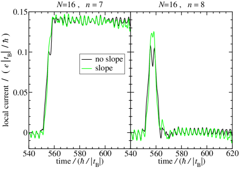
The on-site energies within the ring are all set to the half of the instant bias value. The on-site energy profile within the ring is spatially constant. One may expect that the results would be different if we had considered spatial variation of the on-site energies within the ring. The energies might, for example, be computed on-the fly as dependent on the electron charge density which would be a simple dynamical mean-field model. Another model for ring on-site energies may be their linear variation (slope) from one terminal of the ring to the opposite terminal such that the on-site energies of the vertex atoms reach those in the corresponding leads. We checked both these models and found that they do not have any significant impact on the electron dynamics in the tested cases. This is illustrated in Fig. 7 for a ring composed of 16 atoms and the drain vertex being either at site (conducting configuration) or at site (insulating configuration). As we can see the differences between the spatially uniform and the spatially varying model are essentially negligible for both conducting and insulating configurations. This finding may not be universally valid. However, to keep the models in the present work simple, we stick at the spatially uniform profile of on-site energies within the studied rings, with obvious exceptions of an applied gate potential (see Sec. 6.3).
6.2 Circulating currents
It has been discussed in several studies (e.g. [21]) that circulating currents (CCs) may arise in certain ring configurations. These analysis were done for stationary currents. In this subsection we study circulating currents in transient regime upon the abrupt switch of the bias. By definition, a CC at given instant of time in a ring structure (like that on Fig. 1) exists when the currents in the two ring branches have opposite directions in the sense that, for example, the electrons in the shorter branch flow from the left terminal to the right one while the electrons in the longer branch flow from the right terminal to the left one. The currents in the ring branches are calculated using formulae (18) and (17). These formulae represent strictly local currents: is in fact the current between sites and , i.e. a current through the bond. Our calculation of the current in given ring branch in addition involves averaging over the interatomic bonds of given branch.
Inspection of the currents calculated from exact transmittances of Ref. [23] shows that stationary CCs are possible for many ring sizes. Actual occurrence of the CCs depends also on chosen drain site and on applied bias. Of the studied rings we found most pronounced CC in ring with its drain vertex at site and .
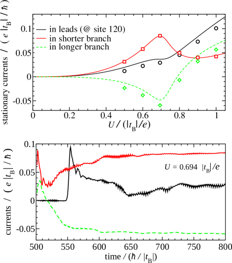
The results for the structure are shown in Fig. 8.
Upper panel in Fig. 8 shows the exact stationary electron currents, calculated with the approach described in [23] (lines), alongside with the quasi-stationary values from our simulations computed with the basis-set parameter (isolated symbols) [43]. Red (dark grey solid line) and green (light grey dashed line) plots display currents in the two ring branches and are relevant in verifying if CC is present. The sign convention used on the figure is such that currents in both branches have positive signs for the flow of the particles from left to right, i.e. state without CCs. The negative value of one of the currents indicates the presence of the CC in the ring. From the upper panel of Fig. 8 we see that such a negative electron current flows in stationary regime in the longer ring branch for a wide range of voltages (0 to ). Most pronounced CC is found at a bias of .
Lower panel of Fig. 8 extends the results at the bias into the non-stationary regime. The non-stationarity is due to the abrupt bias switch at time . The colour and sign convention is the same as for the upper panel. Negative currents show up in the longer ring branch. Black plot on the lower panel of Fig. 8 represents current computed at site 120 (i.e. the usual current in the right lead at a position 115 sites beyond the right vertex atom)222The smoothening of the artificial oscillations (see previous footnote) is not always perfect as can be seen from the bottom panel of Fig. 8, especially the black and red plots. This is a purely technical issue caused by a too large interval between recorded data from the simulation and by the width of the window used to compute the running averages. It is interesting that the green plot in the graph does not show the oscillations. In fact they are present but are very small in magnitude. The impact of the finite basis set on the presence of the oscillations is often quantitatively different in different parts (leads and ring branches) of the whole system..
Finally, the dip in the right-lead current (black plot on the lower panel of Fig. 8) at times ranging from about 630 to is caused by the numerical cutoff on the stroboscopic basis set size. This unphysical dip tends to be more pronounced in certain ring configuration, for certain quantities and for high biases. Ring configuration is significantly affected by the finite basis set error at certain time interval. This is also the reason why we used parameter to obtain results shown in Fig. 8 while for most of other figures we use . The increased cutoff improves accuracy of time-dependences especially at intermediate times.
6.3 Time-dependent currents controlled by gate field
Quantum interference effects between electrons in the two ring arms can be controlled by an applied electric field. The field value can be time-dependent in general. In our approach it is modelled by a spatially uniform lift of on-site energies in one of the branches of the ring (not including the two terminal atoms); the affected atoms have indices , , …, in the indexing scheme of Fig. 1.
6.3.1 Abrupt gate turn-on
In our first studied application of the gate potential, we control the electron transport using an instantaneously switched gate field which is applied to the two rings differing by their drain terminal indices . The field is turned on at time , after the system has been evolving under the constant bias of so that it is essentially in a stationary-current regime before the time when the gate field is lifted. The simulations give results which are depicted in Fig. 9.
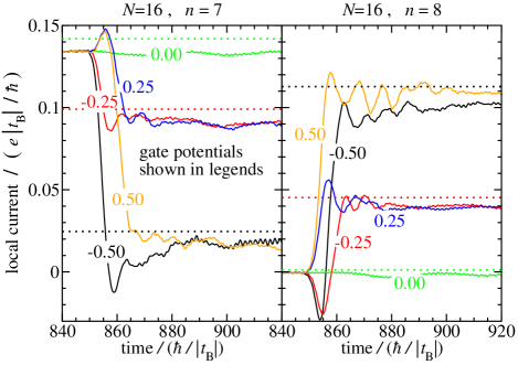
The local current is evaluated at the lattice site 120. We observe that the gate field induces transient effects lasting for about time units. The transient effects depend rather strongly on particular bias values. The application of the higher gate field is interesting; it would allow the ring to work as a field driven switching device, i.e. a nanoscale-sized transistor, changing the conducting ring into non-conducting or vice versa. The switching is a consequence of effective change in Fermi wavelength of electrons in the controlled (longer) branch and hence changing the interference pattern which shows up in the resulting current. The dynamically computed currents at longer times agree well with the exact values from eigenstates although differences arise especially at higher gate potentials. As in other calculations, the source of the differences is the finite cutoff on the number of stroboscopic basis packets used.
6.3.2 Harmonic gate potential
Another option to control the current flow is to employ a harmonically oscillating gate potential. For this purpose we decided to use larger rings with sizes ranging from 70 to 90. Such rings provide longer characteristic times of temporal changes. We study the following three configurations: , , and . All the three rings thus have one longer and one shorter branch. The gate field is again applied to atoms with indices in the range , …, , i.e. the atoms of the shorter branch now. The constant bias is again . The magnitude of the sinusoidal gate potential is always . The potential is harmonic with various angular frequencies as shown on Fig. 10.
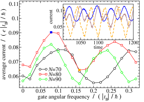
The potential starts to act at time . The inset of Fig. 10 shows typical time dependencies of the current in leads as obtained for the case . The three plots of the inset have been recorded for three different gate angular frequencies : (dark blue, solid line), (brown, solid line) and of (orange, dashed line). The corresponding periods are approximately , , and of . The current response is generally quasi-periodic but anharmonic. (The initial transient effect after the gate is turned on is not discussed here.) The temporal dependence of the current is given by an interplay of the harmonic gate potential and internal ring effects given also by its size. At low gate frequencies (for example or less, see the blue plot, dark solid line, in the inset), the current oscillations typically (not always) exhibit periodic quasi-harmonic pattern at the twice of the gate frequency. The doubled frequency arises from the symmetric dependence of the system transmittance on the gate potential. ( and have the same effect on stationary currents as could be seen from the analytic formulae of Ref. [23] or calculated by formalism of Sec. 5.) Rapid driving is not followed by the current in this sense as can be seen from the inset. For example, the gate field with (the orange plot with dashed line on the figure) or at higher gate frequencies results in current oscillations at the same frequency. Intermediate driving frequencies (e.g. , the brown plot, solid line, on the figure) yield periodic but anharmonic time dependences.
It is interesting to compute time averages from the oscillating lead currents. The three plots in the main graph of Fig. 10 show that the average current for given ring structure depends on the gate frequency (while the bias and the gate amplitude are kept unchanged). The maxima and minima of the average currents vary with varying ring structure: larger rings have the extrema shifted towards lower frequencies. Inspection of the plots show that these variations fulfil the law which is expected from elementary considerations about resonant frequencies. In this way we have an evidence that the oscillatory pattern of the average current plotted in Fig. 10 arises from the internal ring resonances. Given the nanometer-scale size of such ring structures, the characteristic resonant frequencies lie in the optical domain and we do not investigate higher gate frequencies that those shown in the graph.
Electric current dynamics could be investigated also for a fixed ring size and varying drain terminal . However, our inspection has shown that the dynamics is more interesting (i.e. the average currents exhibit more pronounced oscillations as functions of ) when the source and drain terminal are relatively close to each other.
6.4 Reduced coupling to the leads
Through previous sections it was assumed that all nearest neighbour couplings were identical along the whole composed system, i.e. including the small system (the ring). The couplings between the leads and the ring were then quantified by the hopping parameter (same as in the lead and in the ring).
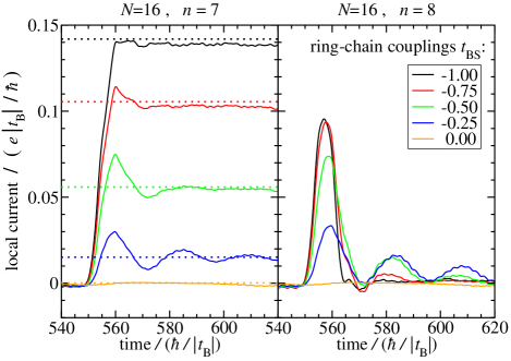
In this section we study a more general situation when the couplings within the leads again remain equal to and the same parameter is used also to bound the atoms included in the ring. The couplings between the leads and the ring will however be characterised by a new parameter (lead-system coupling).
We will report on regimes with . In the limiting case of the leads and the system (the ring) become decoupled and the internal energy levels of the ring attain discrete values. In intermediate cases of we expect broadening of the ring levels. The internal ring electronic structure will have an impact on the transport characteristics.
An illustration of our findings is shown on Fig. 11. The time-dependent currents have been computed for the rings of atoms, left panel corresponding to drain vertex site (conducting configurations) while right panel shows plot for (insulating configurations). In all cases the bias was abruptly switched on at time . The magnitude of the transient effect as well as the currents (in the conductive system) behave as expected regarding to the lead-system coupling strength. The insulating ring retains its property also at reduced couplings. However, at intermediate coupling range , there are decaying oscillations in the electron current persisting for a significant period of time, thus extending the transient effect to a period of about . Inspection shows that angular frequency of these decaying oscillations is related to the applied bias by the relation , in agreement with previous analytical [17] as well as numerical [7] results.
7 Conclusions
Recently proposed stroboscopic wave packets [16, 17] have been developed to be applicable to systems employing explicit atomistic level of modelling. Time-dependent transport of electrons in an open system with localised perturbation was studied. The localised perturbation had a ring structure described in the tight-binding approximation. Such a system is of interest due to quantum interference effects that affect its transport properties. It might serve as a field driven quantum interference current switching device [36] – a nanoscale-sized transistor. We have demonstrated the potential of our newly developed method based on the unitarily propagating stroboscopic wave packets to describe open systems with fluctuating number of explicitly included electrons while the whole system has an infinite number of electrons which can be neglected in a good approximation. In our method full quantum coherence is preserved throughout the whole infinite system. The method can be used for systems with one-dimensional semi-infinite leads. It is capable of spatially resolved description of transient effects like those caused by an abrupt bias switch of a gate field application. However, its most useful application would be found in systems which are exposed to long-lasting varying external fields or biases and for which it is important to preserve quantum coherence in the description. For short-time simulations one could use a less expensive model with cyclic boundary conditions. However, such an approach would become prohibitively expensive for large simulation times as it would require to consider many explicit atoms to describe the leads. In contrast, our method does not have any such limit on simulation time. The weakness of the present implementation of the stroboscopic basis set description is slow convergence of relevant results with increasing number of basis functions. The finite basis set demonstrates itself in a transient unphysical drop of lead current in some of the studied systems. Depending on the studied configuration, long-time stationary currents may also sometime be significantly underestimated. Other consequence of the finite stroboscopic basis set are small artificial rapid oscillations in computed quantities which can however be smoothed out and usually does not prevent us from capturing relevant physical time-dependent effects. In our ongoing work we will consider a generalisation of the basis set in order to reduce the finite-basis set errors and to reduce the number of basis states needed.
8 Acknowledgements
This work was supported in parts by the Slovak Grant Agency for Science (VEGA) through grant No. 1/0632/10 and by the Slovak Research and Development Agency under the contract No. APVV-0108-11.
References
- [1] H. Haug and A.-P. Jauho, Quantum Kinetics in Transport and Optics of Semiconductors (Springer-Verlag, Berlin, Germany, 1998)
- [2] H. Ness and L.K. Dash, Phys. Rev. B 84, 235428 (2011)
- [3] M. Cini, Phys. Rev. B 22, 5887 (1980)
- [4] G. Stefanucci and C.-O. Almbladh, Phys. Rev. B 69, 195318 (2004)
- [5] See for example S. Kurth, G. Stefanucci, C.-O. Almbladh, A. Rubio, and E.K.U. Gross, Phys. Rev. B 72, 035308 (2005) and the references therein
- [6] P. Myöhänen, A. Stan, G. Stefanucci, and R. van Leeuwen, Phys. Rev. B 80, 115107 (2009)
- [7] B. Wang, Y. Xing, L. Zhang and J. Wang, Phys. Rev. B 81, 121103 (2010)
- [8] Y. Wang, C.Y. Yam, G.H. Chen, Th. Frauenheim, and T.A. Niehaus, Chem. Phys. 391, 69 (2011)
- [9] X. Zheng, F. Wang, C.Y. Yam, Y. Mo, and G. Chen, Phys. Rev. B 75, 195127 (2007)
- [10] H. Xie, F. Jiang, H. Tian, X. Zheng, Y. Kwok, S. Chen, C. Yam, and G. Chen, J. Chem. Phys. 137, 044113 (2012)
- [11] K. Torfason, A. Manolescu, V. Molodoveanu, and V. Gudmundsson, J. Phys.: Conf. Series 338, 012017 (2012)
- [12] P. Hyldgaard, J. Phys.: Condens. Matter 24, 424219 (2012)
- [13] A.P. Horsfield, D.R. Bowler, and A.J. Fisher, J. Phys.: Condens. Matter 16, L65 (2004)
- [14] E.J. McEniry, D.R. Bowler, D. Dundas, A.P. Horsfield, C.G. Sánchez, and T.N. Todorov, J. Phys.: Condens. Matter 19, 196201 (2007)
- [15] E.J. McEniry, Y. Wang, D. Dundas, T.N. Todorov, L. Stella, R.P. Miranda, A.J. Fisher, A.P. Horsfield, C.P. Race, D.R. Mason, W.M.C. Foulkes, and A.P. Sutton, Eur. Phys. J. B 77, 305 (2010)
- [16] P. Bokes, F. Corsetti, and R.W. Godby, Phys. Rev. Lett. 101, 046402 (2008)
- [17] P. Bokes, Phys. Chem. Chem. Phys. 11, 4579 (2009)
- [18] J. Yi, G. Cuniberti, and M. Porto, Eur. Phys. J. B 33, 221 (2003)
- [19] F. Goyer, M. Ernzerhof, and M. Zhuang, J. Chem. Phys. 126, 144104 (2007)
- [20] B.T. Pickup and P.W. Fowler, Chem. Phys. Lett. 459, 198 (2008)
- [21] G. Stefanucci, E. Perfetto, S. Bellucci, and M. Cini, Phys. Rev. B 79, 073406 (2009)
- [22] J.-B. Xia, Phys. Rev. B 45, 3593 (1992)
- [23] R.E. Sparks, V.M. García-Suárez, D.Zs. Manrique, and C.J. Lambert, Phys. Rev. B 83, 075437 (2011)
- [24] K.K. Saha, B.K. Nikolić, V. Meunier, W. Lu, and J. Bernholc, Phys. Rev. Lett. 105, 236803 (2010)
- [25] K.K. Saha, W. Lu, J. Bernholc, and V. Meunier, J. Chem. Phys. 131, 164105 (2009)
- [26] M. Kiguchi, O. Tal, S. Wohlthat, F. Pauly, M. Krieger, D. Djukic, J.C. Cuevas, and J.M. van Ruitenbeek, Phys. Rev. Lett. 101, 046801 (2008)
- [27] M. Kiguchi, S. Nakashima, T. Tada, S. Watanabe, S. Tsuda, Y. Tsuji, and J. Terao, Small 8, 726 (2012)
- [28] M. Bai, J. Liang, L. Xie, S. Sanvito, B. Mao, and S. Hou, J. Chem. Phys. 136, 104701 (2012)
- [29] W. Hong, H. Li, S.-X. Liu, Y. Fu, J. Li, V. Kaliginedi, S. Decurtins, and T. Wandlowski, J. Am. Chem. Soc. 134, 19425 (2012)
- [30] X. Li, X. Wang, L. Zhang, S. Lee, and H. Dai, Science 319, 1229 (2008)
- [31] X. Wang, Y. Ouyang, X. Li, H. Wang, J. Guo, and H. Dai, Phys. Rev. Lett. 100, 206803 (2008)
- [32] M.A. Reed, C. Zhou, C.J. Muller, T.P. Burgin, and J.M. Tour, Science 278, 252 (1997)
- [33] B. Hackens, F. Martins, T. Ouisse, H. Sellier, S. Bollaert, X. Wallart, A. Cappy, J. Chevrier, V. Bayot, and S. Huant, Nature Physics 2, 826 (2006)
- [34] F. Martins, B. Hackens, M.G. Pala, T. Ouisse, H. Sellier, X. Wallart, S. Bollaert, A. Cappy, J. Chevrier, V. Bayot, and S. Huant, Phys. Rev. Lett. 99, 136807 (2007)
- [35] W. Lei, C. Notthoff, A. Lorke, D. Reuter, and A.D. Wieck, Appl. Phys. Lett. 96, 033111 (2010)
- [36] D.M. Cardamone, C.A. Stafford, and S. Mazumdar, Nano Lett. 6, 2422 (2006)
- [37] Stroboscopic wavepacket method can in general work with arbitrary bulk (or even non-periodic) Hamiltonian. The bands need not be two and they need not be equally wide. Our implementation is quite general with respect to the division of Hamiltonian energy spectrum into this kind of bands. In all calculations in this work we however use two equally wide bands because such setup is most practical.
- [38] In actual simulations we use a rather conservative criterion for electron removal. Consequently, no electron is removed during simulated timescales.
- [39] Studies of e-e interactions in connection with quantum interference effects have been published, see for example P. Stefański, J. Phys.: Condens. Matter 22, 505303 (2010).
- [40] W.H. Press, S.A. Teukolsky, W.T. Vetterling, and B.P. Flannery, Numerical recipes in C, 2nd edn. (Cambridge University Press, Cambridge 1994)
- [41] For example, we have in the left lead and in the ring.
- [42] Inspection of the currents through branches of unsymmetrical rings shows that the situation is more complicated inside such rings. See Fig. 8 as an example.
- [43] Here we could equivalently use our exact-eigenstate method described in Sec. 5. We instead used formulas of Ref. [23] because of their convenience.
Appendix A Derivation of the overlaps
Here we derive formula (14) for the overlaps between the TB atomic orbitals and the SWPs . In the SWPA [16, 17], the eigenstates of the basis-generating Hamiltonian [given by eq. (2) in this work] use the energy “normalisation” condition which is
| (26) |
See also sec. 3 and eq. (5) therein. This condition leads to the form
| (27) |
where is the usual Bloch wave in one dimension with the k-number of magnitude and the propagation direction labelled by . Normalisation of the Bloch waves is assumed to be
| (28) |
(The k-numbers will be restricted to the interval where is the lattice constant.) In case of the TB model with the set of the orthonormal atomic orbitals (one orbital per atom) we obtain formula
| (29) |
with the summation running over all lattice sites. is the dimensionless wavenumber. The eigenstates are used to construct the SWPs according to eq. (5). Now we use that formula and write down the overlaps in the form
| (30) |
where we have utilised the equation
| (31) |
Using the expression (29) for the eigenstates and substituting it into eq. (30) leads to an integral expression with integration variable . With the aid of the TB dispersion relation (6), the integral can be transformed to the integration variable . The final form of the expression for the overlap is then provided by formula (14). We evaluate these integrals numerically.