Spin filter effect at room temperature in GaN/GaMnN ferromagnetic resonant tunnelling diode.
Abstract
We have investigated the spin current polarization without the external magnetic field in the resonant tunneling diode with the emitter and quantum well layers made from the ferromagnetic GaMnN. For this purpose we have applied the self-consistent Wigner-Poisson method and studied the spin-polarizing effect of the parallel and antiparallel alignment of the magnetization in the ferromagnetic layers. The results of our calculations show that the antiparallel magnetization is much more advantageous for the spin filter operation and leads to the full spin current polarization at low temperatures and 35 % spin polarization of the current at room temperature.
The progress in homo- and heteroepitaxy of dilute magnetic semiconductorsKoo2010 ; Agarwal2006 ; Edmonds2002 ; Yu2002 ; Chiba2003 ; Ku2003 ; Eid2005 ; Jungwirth2005 (DMS’s) during the past decade allows to fabricate spintronic nanodevices, in which the spin polarization of the current can be controlled by the magnetic or electric field. The spin filter effect in a resonant tunneling diode (RTD) with paramagnetic quantum well embedded in II-VI DMS (ZnMnSe) was studied theoreticallyWojcik2012 ; Wojcik2012JAP ; Wojcik2012SST and experimentally demonstrated by Slobodskyy et al.Slobodskyy2003 For the paramagnetic RTD, in the presence of the external magnetic field, the exchange interaction between the conduction band electrons and the Mn2+ ions leads the giant Zeeman splittingFurdyna1988 of the quasi–bound state in the paramagnetic quantum-well. This splitting causes that the resonance conditions for the spin up and spin down electrons are satisfied for different bias voltages leading to the separation of the spin current components and consequently to the spin polarization of the current. The spin filter effect in the paramagnetic RTD is limited to very low temperature and requires the high external magnetic field.Slobodskyy2003 ; Furdyna1988 These restrictions cause that more interest is directed towards the application of the ferromagnetic III-V semiconductors, especially those with high Curie temperature, e.g. GaMnAsJungwirth2005 ; Wang2005 ; Panguluri2004 ; Csontos2005 or GaMnN.Dietl2000 ; Liu2005 Ohno et al.Ohno1998 experimentally studied the ferromagnetic RTD based on GaMnAs in which the spin splitting was observed without external magnetic field but it still requires low temperature. Hovewer, the recent experiments reported that GaMnN can exhibit the ferromagnetic properties above room temperatureSasaki2002 ; Ando2003 ; Pearton2007 at which the exchange splitting of the conduction band is about few tens of meVErtler2007 and remains in the limit of thin layer of a few nanometer width.Priour2005 Although the ferromagnetism in GaMnN is still unresolved theoretical problem, the spin filter effect in the RTD’s based on GaMnN is a subject of research carried out by many groups. Recently, Li et al.Li2006 have theoretically investigated the ferromagnetic RTD consisted of the InGaN quantum well between two GaMnN barriers. In Ref. Li2006, the spin polarization of the current without magnetic field has been predicted at low temperature but at room temperature it has been reduced to only 8 %. Another way to obtain the spin polarization of the current at room temperature was proposed by Qui el at.Qui2008 who stated that the doping of the GaN quantum well in the RTD with ferromagnetic (GaMnN) contacts enhances the spin polarization of the current by two times. The double enhancement of the spin polarization at room temperature was also reported by Wang et al.Wang2009 who investigated the influence of the charge polarization at the interface AlGaN/GaN in RTD with ferromagnetic contacts embedded in GaMnN.
In the present paper, we propose the RTD structure with the ferromagnetic emitter and quantum well regions made from GaMnN. Based on self-consistent Wigner-Poisson calculations we predict the full spin polarization of the current (i.e. ) at low temperature for antiparallel magnetization of the magnetic layers. The spin polarization reduces to at room temperature. To the best of our knowledge, this is the highest value of the spin polarization predicted at room temperature in magnetic RTD. In particular it is about four times higher than that reported by Li et al. Li2006 We also showe that the proposed ferromagnetic RTD structure with the antiparallel alignment of magnetization can lead to the fairly large spin polarization of the current at room temperature.
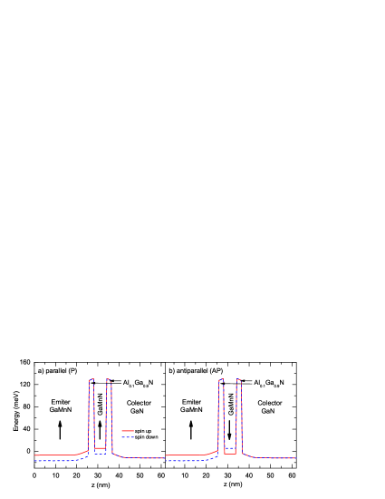
We investigate the ferromagnetic RTD based on GaN/Al1-xGaxN/GaMnN with the emitter and quantum well layer made from GaMnN (Fig. 1). The parallel (P) and antiparallel (AP) alignments of the magnetization of the emitter and quantum well is considered. The conduction band profiles at zero bias for spin up and spin down electrons are presented in Fig. 1. The calculations have been performed with the following nanostructure parameters: the thickness of the GaMnN quantum well layer is 6 nm, the barriers are assumed to be symmetric with thickness 3 nm and yields the barrier height 130 meV. Ambacher2002 We assume the conduction-band electrons of GaN, i.e., m/m0 = 0.228 and take on the relative electric permittivity = 8.6. In order to describe the pure spin filter effect in the proposed ferromagnetic nanostructure we neglect the charge polarization occurring at the interface AlGaN/GaN.Ambacher2002
Our numerical calculations are based on the Wigner-Poisson approach, according to which the conduction band electrons are described by the spin dependent Wigner distribution function (WDF). Assuming the translational invariance in the plane and neglecting the spin scattering (many transport experiments showed that the spin scattering lenght is compared to the size of the RTDOhno1998 ; Ohya2005 ) the time independent quantum transport equations can be reduced to the following one-dimensional form:Spisak2009
| (1) |
where is the spin-dependent WDF, is the
-component of the wave vector and is the spin index.
The non-local potential in Eq. (1) is
given by the formula
| (2) |
where is the spin-dependent potential energy profile, which
can be expressed as the sum of the three terms
,
where consecutive terms denote the spin-dependent conduction-band potential energy,
the electrostatic potential energy calculated by solving the Poisson equation
and the exchange energy.
Equations (1) and the Poisson equation form the system of non-linear integro-differential equations
that is solved by the self-consistent procedure.Wojcik2012
After reaching convergence the spin dependent current density is calculated using the formula
| (3) |
where is the length of the nanodevice.
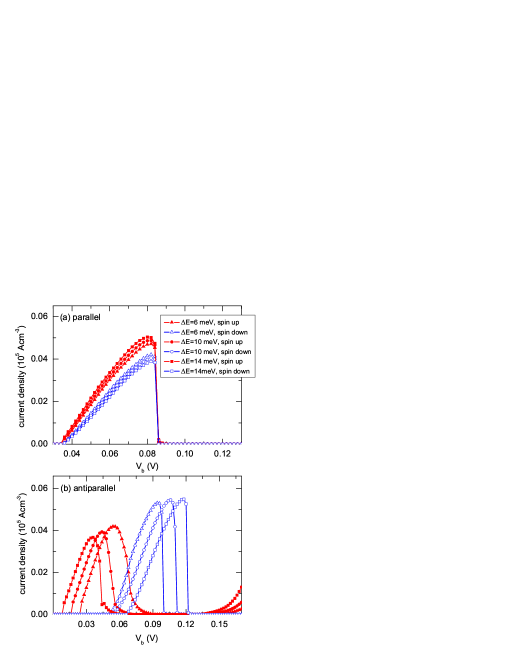
The ferromagnetic properties of GaMnN causes that the spin-degenerate quasi-bound state energy level in the quantum well splits into two levels for spin up and spin down electrons. Similarly, the conduction band in the ferromagnetic emitter layer is splited into two subbands for different spins. The spin splitting of the conduction bands in the ferromagnetic layers causes that the resonance transport conditions are different for the electrons with different spins. In the present calculations the spin splitting energy of of the conduction band is treated as an parameter of calculations that varies from 2 meV to 15 meV (the reliable values reported in experiments Dietl2000 ; Liu2005 ). Fig. 2 shows the spin-dependent current-voltage characteristics calculated at temperature K for (a) parallel and (b) antiparallel alignment of the magnetization of the emitter and the quantum well layers.
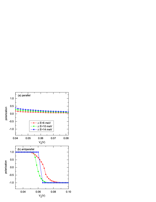
We see that for the parallel magnetization of the layers the resonant current peaks for spin up and spin down current component occur at almost the same bias . If the splitting energy increases, the resonant current peak increases for spin up and decreases for spin down current component. On the other hand for the antiparallel magnetization of the magnetic layers the resonant current peaks for both the spin components behave in a different manner. Namely, the increasing causes the separation of the resonant current peaks: the resonant peak for the spin up current component shifts towards the lower bias while the resonant peak for the spin down current component shifts towards the higher bias. The separation of the spin current components leads to the spin polarization of the current defined as . In Fig. 3 we present the spin polarization of the current as a function of the bias calculated for (a) parallel and (b) antiparallel alignment of the magnetization of the ferromagnetic layers. We see that for the parallel magnetization the spin polarization of the current is positive at the low bias and decreases with increasing the bias. On the other hand for the antiparallel magnetization of the ferromagnetic layers the spin polarization of the current varies from for the low bias to for the high bias. This dependence is observed for all values of the splitting energy , however, for the higher the transition between both the fully polarized states occurs in a narrower bias range.
In order to explain strongly polarizing effect of the ferromagnetic RTD with the antiparallel magnetization of the ferromagnetic layers we present the simple model of the spin dependent electron transport through the RTD for both alignments of the magnetization (Fig. 4).
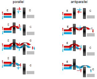
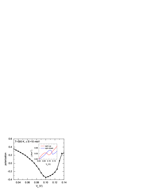
Fig. 4 shows that only the antiparallel alignment of the magnetization can lead to the full spin polarization of the current. Let us note that at room temparature the transport window in the magnetic emitter broadens in the nearest of the Fermi energy. This thermal effect causes the broadenning of the resonant current peak for spin up and spin down current components (inset in Fig. 5). Our calculations show that even for small but experimental realiable value of the splitting energy meV the spin polarization at room temperature is still quite large and achieves (Fig. 5). This value is four times larger than that reported in Ref. Li2006, .
Moreover we expect that for the larger splitting energy , the antiparallel magnetization of the magnetic layers can lead to the full spin polarisation of the current at room temperature.
In conclusion, we have shown that the antiparallel alignment of the magnetization in the ferromagnetic resonant tunneling structure with the ferromagnetic emitter and quantum well can be used to obtain the full spin polarization of the current at room temperature. Our theoretical calculations predicts that the spin polarization of the current in the ferromagnetic RTD based on GaMnN achieves at room temperature for experimentally reported splitting energy meV in GaMnN. We also argue that proposed nanostructure can allow to increase the polarization up to at room temperature for sufficiently large splitting energy . The achievement of the full spin current polarisation at room temperature by increasing of is a challenge for the future spintronic technology which allows to construct the effective spin filter working at room temperature.
This paper has been supported by the Polish Ministry of Science and Higher Education and its grants for Scientific Research.
References
- (1) T. K. Koo, O. Byungsung, Y. M. Yu, D. J. Kim, C. S. Kim, Y. D. Choi, J. W. Lee, M. Y. Yoon, P. Y. Yu, and T. W. Kang, J. Appl. Phys. 108, 113508 (2010)
- (2) K. C. Agarwal, B. Daniel, C. Klingshirn, and M. Hetterich, Phys. Rev. B 73, 045211 (2006)
- (3) K. W. Edmonds, K. Y. Wang, R. P. Campion, A. C. Neumann, N. R. S. Farley, B. L. Gallagher, and C. T. Foxon, Appl. Phys. Lett. 81, 4991 (2002)
- (4) K. M. Yu, W. Walukiewicz, T. Wojtowicz, I. Kuryliszyn, X. Liu, Y. Sasaki, and J. K. Furdyna, Phys. Rev. B 65, 201303 (2002)
- (5) D. Chiba, K. Takamura, F. Matsukura, and H. Ohno, Appl. Phys. Lett. 82, 3020 (2003)
- (6) K. C. Ku, S. J. Potashnik, R. F. Wang, S. H. Chun, P. Schiffer, N. Samarth, S. M. J, A. Mascarenhas, E. Johnston-Halperin, R. C. Myers, A. C. Gossard, and D. D. Awschalom, Appl. Phys. Lett. 82, 2302 (2003)
- (7) K. F. Eid, B. L. Sheu, O. Maksimov, M. B. Stone, P. Schiffer, and N. Samarth, Appl. Phys. Lett. 86, 152505 (2005)
- (8) T. Jungwirth, K. Y. Wang, J. Masek, K. W. Edmonds, J. König, J. Sinova, M. Polini, N. A. Goncharuk, A. H. MacDonald, M. Sawicki, A. W. Rushforth, R. P. Campion, L. X. Zhao, C. T. Foxon, and B. L. Gallagher, Phys. Rev. B 72, 165204 (2005)
- (9) P. Wójcik, J. Adamowski, M. Wołoszyn, and B. J. Spisak, Phys. Rev. B 86, 165318 (2012)
- (10) P. Wójcik, B. J. Spisak, M. Wołoszyn, and J. Adamowski, J. Appl. Phys. 111, 124310 (2012)
- (11) P. Wójcik, B. J. Spisak, M. Wołoszyn, and J. Adamowski, Semicond. Sci. Technol. 27, 115004 (2012)
- (12) A. Slobodskyy, C. Gould, T. Slobodskyy, C. R. Becker, G. Schmidt, and L. W. Molenkamp, Phys. Rev. Lett. 90, 246601 (2003)
- (13) J. K. Furdyna, J. Appl. Phys. 64, R29 (1988)
- (14) K. Y. Wang, K. W. Edmonds, R. P. Campion, B. L. Gallagher, N. R. S. Farley, T. Foxon, M. Sawicki, P. Boguslawski, and T. Dietl, J. Appl. Phys. 95, 6512 (2005)
- (15) R. P. Panguluri, B. Nadgorny, T. Wojtowicz, W. L. Lim, X. Liu, and J. K. Furdyna, Appl. Phys. Lett. 84, 4947 (2004)
- (16) M. Csontos, G. Mihaly, B. Janko, B. Wojtowicz, X. Liu, and F. J. K, Nat. Mater. 4, 447 (2005)
- (17) T. Dietl, H. Ohno, F. Matsukura, J. Cibert, and D. Ferrand, Science 287, 1019 (2000)
- (18) C. Liu, F. Yun, and H. Morkor, J. Mater. Sci.: Mater. Electron. 16, 555 (2005)
- (19) H. Ohno, N. Akiba, F. Matsukura, A. Shen, K. Ohtani, and Y. Ohno, Appl. Phys. Lett. 73, 363 (1998)
- (20) T. Sasaki, S. Sonda, Y. Yamamoto, K. Suga, S. Shimizu, K. Kindo, and H. Hori, J. Appl. Phys. 91, 7484 (2002)
- (21) K. Ando, Appl. Phys. Lett. 82, 100 (2003)
- (22) S. Pearton, D. Norton, M. Ivill, A. Hebard, J. Zavada, W. Chen, and Buyanova, J. Electron. Mater. 36, 462 (2007)
- (23) C. Ertler and J. Fabian, Phys. Rev. B 75, 195323 (2007)
- (24) D. J. Priour Jr., E. H. Hwang, and S. Das Sarma, Phys. Rev. Lett. 95, 37201 (2005)
- (25) M. K. Li, N. M. Kim, S. J. Lee, H. C. Jeon, and T. W. Kang, Appl. Phys. Lett. 88, 162102 (2006)
- (26) Z. J. Qui, S. L. Zhang, and L. R, Appl. Phys. Lett. 92, 242110 (2008)
- (27) J. Wang, Y. Liu, H. Mao, Q. Zhao, Y. Jianguo, Y. Zhang, Z. Zhu, and J. Chu, Appl. Phys. Lett. 94, 172501 (2009)
- (28) O. Ambacher, J. Majewski, C. Miskys, A. Link, M. Herman, M. Eickhoff, M. Stutzmann, F. Bernardini, V. Fiorentini, V. Tilak, B. Schaff, and L. F. Eastman, J. Phys. Condens. Matter 14, 3399 (2002)
- (29) S. Ohya, P. N. Hai, and E. Y. Tanaka, Appl. Phys. Lett. 87, 012105 (2005)
- (30) B. J. Spisak, M. Wołoszyn, P. Wójcik, and G. J. Morgan, J. Phys.: Conf. Ser. 193, 012130 (2009)