The order-parameter symmetry and Fermi surface topology of 122 Fe-based superconductors: a point-contact Andreev-reflection study
Abstract
We report on the results of directional point-contact Andreev-reflection (PCAR) measurements in single crystals and epitaxial -axis oriented films with as well as in single crystals with . The PCAR spectra are analyzed within the two-band 3D version of the Blonder-Tinkham-Klapwijk model for Andreev reflection we recently developed, and that makes use of an analytical expression for the Fermi surface that mimics the one calculated within the density-functional theory (DFT). The spectra in unambiguously demonstrate the presence of nodes or zeros in the small gap. In , the -plane spectra in single crystals can be fitted by assuming two nodeless gaps, but this model fails to fit the -axis ones in epitaxial films. All these results are discussed in comparison with recent theoretical predictions about the occurrence of accidental 3D nodes and the presence of “hot spots” in the gaps of 122 compounds.
I Introduction
Four years after the discovery of superconductivity in Fe-based compounds kamihara08 , a surprising variety of behaviors has been unveiled not only between compounds of different classes (the so-called 1111, 11 or 122 classes, just to mention the most studied) but also among compounds of the same class that share the same crystal structure. One of the properties that shows unexpected variations in a given class of Fe-based pnictides is the symmetry of the order parameter(s) (OPs) so that it is not possible to make a general statement about the gap symmetry of these compounds. The multiband electronic structure and the Fermi surface (FS) nesting that is responsible for the antiferromagnetic instability in the parent compounds strongly suggest a superconducting pairing mediated by spin fluctuations mazin08 ; mazin10b which is also supported by many experimental facts paglione10 . Various possible gap symmetries are allowed, at least theoretically, within the picture of spin-fluctuation mediated pairing. In most of optimally-doped compounds the so-called symmetry with isotropic OPs of opposite sign on the holelike and electronlike FS sheets is realized mazin08 , but the emergence of nodes or zeros on some FSs is theoretically predicted in various situations mazin10 ; kuroki09 ; suzuki11 .
Here we report on recent PCAR spectroscopy results in single crystals of 8% Co-doped BaFe2As2 (Ba-122) with bulk K and in single crystals of 6 % Co-doped CaFe2As2 (Ca-122) with K. In the first case, the PCAR spectra (taken with the current injected along the planes) are compatible with two nodeless gaps of different amplitude, the smaller being probably associated to one of the electrolike FS sheets, in agreement with angle-resolved photoemission spectroscopy (ARPES) terashima09 . In the crystals of Co-doped Ca-122, the PCAR spectra systematically show a zero-bias peak or maximum, which strongly suggests that the small gap (residing here on the holelike FS sheet centered at the point of the Brillouin zone) presents lines of nodes or zeros on the FS, while the large gap remains presumably isotropic. This finding agrees with the predictions about the emergence of 3D nodes in the OP of 122 compounds when the holelike FS evolves towards a topological transition from a warped cylinder to separate pockets suzuki11 ; gonnelli12 . Finally, we present new results of PCAR experiments in epitaxial thin films of 8% Co-doped Ba-122 (with K). In this case, the current is injected along the axis and the 3D-BTK model with two nodeless gaps fails to fit the PCAR spectra at low energy. This might be a hallmark of the presence of “hot spots” (where the gap is strongly suppressed) or 3D nodal lines on some of the FSs, which has been proposed mazin10 to explain Raman results in this compound muschler09 .
II Experimental details
II.1 The samples
The single crystals (with ) were prepared by the self-flux method sefat08b under a pressure of 280 MPa at the National High Magnetic Field Laboratory in Tallahassee. The crystal size is mm3, and the axis is perpendicular to the larger surface. The resistive transition sets in at K with (10%-90%) = 1 K.
The films (with ) were deposited at the Leibniz Institute for Solid State and Materials Research (IFW) in Dresden, Germany. Two kinds of substrates were used: single-crystalline CaF2 or MgO (in this case, with a Fe buffer layer on top of it). The films are epitaxial with the axis normal to the surface. The superconducting transition of the films on CaF2 has a midpoint at K, while its width is K. For the films on MgO the same quantities are K and K.
The Ca(Fe1-xCox)2As2 single crystals were grown at ETH Zurich from Sn flux, as described in Ref. matusiak10 , and were plate-like, with the axis perpendicular to the plate. The superconducting transition as measured from DC susceptibility sets in at K and an effective K can be determined by extrapolating the linear part of the curve. The transition is rather broad, but this is common to all the state-of-the-art crystals of the same compound grown at present harnagea11 . The broad transition is however not detrimental to point-contact measurements: Simply, the local critical temperature of point contacts can vary from point to point within the transition width.
II.2 Point-contact setup and procedure
The point contacts were made by using the “soft” technique described elsewhere daghero10 , in which the metallic tip used as counterelectrode in the more conventional needle-anvil configuration is replaced by a small drop of Ag paste (m) put on the sample surface. In single crystals the contacts were put on a fresh side surface (exposed by breaking the crystals) so that the current was mainly injected along the planes. In films, the point contacts were put on the top surface. Owing to the film orientation, this means that the probe current was mainly injected along the axis.
The conductance curves vs. of each point contact were obtained by numerically differentiating the measured characteristics. The spectra were then normalized (i.e. divided by the normal-state conductance of the same contact) to allow a comparison to the relevant theoretical models. In single crystals (where the high-bias tails of the spectra at different temperatures are superimposed to one another) we divided by the conductance curve recorded just above the critical temperature of the contact, (defined as the temperature at which the Andreev reflection features disappear). In the case of films, this procedure is impossible because of an abrupt vertical shift of the spectra when the temperature approaches . This shift is related to the transition to the normal state of the portion of the film between the point contact and the voltage electrode chen10b and has nothing to do with the contact itself (a detailed model of this phenomenon will be given in a forthcoming paper). Therefore, the low-temperature experimental spectra were divided by a guess normal state obtained by fitting their high-energy tails with a fourth-order polynomial function, as we did in Ref.gonnelli09a .
III Calculation of the Fermi surface
The FS of the materials under study ( with and with ) was calculated within the Density-Functional Theory (DFT) by using the Elk FP-LAPW Code () and the GGA approach for the exchange correlation potential. To account for the partial substitution of Fe with Co we used a virtual-crystal approximation that indeed works particularly well for the Fe-Co substitution.
The lattice constants used for the calculations in the case of are Å and Å as in Ref.singh08b . The height of the As atom above the Fe layer is Å. The resulting FS is shown in Fig. 1(a). It features two holelike FS sheets at the center of the Brillouin zone (BZ). Both have the shape of warped cylinders whose cross section is maximum at the top and bottom edges of the BZ, but the outer one shows a more marked warping. The situation is somewhat similar to that found in with partial substitution of As with P, as described by Suzuki et al. suzuki11 . The two electronlike FS sheets at the corners of the BZ are also warped cylinders with the characteristic elliptical cross section whose semimajor axis varies along .
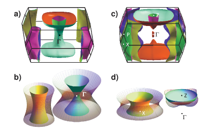
In the case of , there is no direct experimental information on the low-temperature lattice constants. Owing to the small dependence of the room-temperature lattice parameters on the doping content hu11 , we assumed the low-temperature lattice constants of the parent compound in the tetragonal phase to be a good first approximation to the real ones at the doping content of our interest (). We then started from the lattice constants of the orthorhombic phase of at pressure P = 0 calculated as in Ref. colonna11 , and then we made the structure tetragonal by averaging and . The result is Å and Å. These values are in good agreement with the experimental ones measured in the tetragonal phase of at 300 K (and pressure P = 0.8 - 1 GPa mittal11 ). Starting from the calculated equilibrium phase and always considering the antiferromagnetic phase, an optimized parameter Å was obtained. The charge density was thus integrated over points in the Brillouin zone and the band structure as well as the FSs were calculated in the non-magnetic body-centered tetragonal phase. The resulting FS is shown in Fig. 1(c). It is clear that at this doping content the holelike FS sheets are undergoing a topological transition. While at lower doping they have the shape of strongly warped cylinders (similar to those shown for Ba-122 in Fig. 1(a)), at they split into separate cup-shaped pockets centered around the Z points.
IV Results and analysis
IV.1 Ba(Fe1-xCox)2As2 single crystals
Figure 2 presents two examples of experimental normalized conductance curves (symbols) of -plane contacts in single crystals. Both the curves in (a) and (b) show a zero-bias dip, two symmetric maxima related to a small gap, and two other kinks related to a second, larger gap. Moreover, the spectra feature additional, higher-energy structures (indicated by arrows) that are likely to be due to the strong electron-boson coupling tortello10 . We will not deal with these structures here; they cannot be reproduced by any BTK model unless an energy-dependent gap (as obtained from the solution of Eliashberg equations) is used instead of the constant BCS-like gap used here tortello10 ; daghero11 . To fit the experimental curves in Fig. 2 we used the 3D version of the generalized BTK model daghero11 , that accounts for the real shape of the FS and is not based on the simplifying assumption that the latter is spherical or cylindrical, as instead the 1D and 2D BTK models do. For ease of calculation, we used the model FS shown in Fig. 1(b), which mimics the real one from DFT calculations reported in Fig. 1(a). The former consists of two separate hyperboloids of revolution, meant to simulate the main holelike and electronlike sheets, whose radii at the center and at the top (and bottom) of the BZ are in the same proportions as in the real FS, although in Fig. 1(b) the distance between them has been enhanced for clarity. The normalized conductance expected in the case of current injection along the plane can be calculated by using eq. 9 of Ref. daghero11 . Note that, due to the particular mathematical form of the equation, the relative position of the two FS sheets is irrelevant. Of course, the choice of the symmetry of the order parameters that reside on the two hyperboloids is determined by the experiment. In this case, the absence of zero-bias maxima (in all the spectra we measured) suggests that both the gaps are likely to be nodeless, in agreement with ARPES measurements terashima09 . We therefore used in our model two -wave gaps whose amplitudes are pictorially indicated as gridded surfaces in Fig. 1(b). We will call and the large and the small gap, respectively. The 3D BTK model contains 3 adjustable parameters for each band, i.e. the gap amplitude , the broadening parameter and the barrier parameter . The weight of each band in the conductance is not adjustable (as instead happens in the 2D model) being automatically determined by the geometry of the FS and by the barrier parameter . This considerably reduces the uncertainty on the best-fitting parameters.
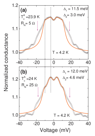
Fig. 2 shows two examples of fit (lines) to the experimental spectra. The values of the parameters are indicated in the caption; the average values are meV and . In the 2D-BTK fit of the same curves the gaps turned out to be meV and meV. With respect to the 2D BTK fit, the 3D one gives smaller values of the small gap and larger values of the large gap, and the theoretical curves are narrower. This is due to the fact that in the 3D model the weight is fixed (in these two cases, the weight of band 1 is about 0.2). Indeed, the 2D fit can be forced to follow the experimental curve at energies higher than 13 meV (where the 3D fit fails) if the weight of the bands is kept around 0.5, but this clearly would not reflect the real shape of the FS sheets. The inability of the model to reproduce the higher-energy structures (in particular the kinks at about 20 meV) simply confirms that these structures are related to effects that are not accounted for by the model (and indeed can be explained as being due to the strong electron-boson coupling, as shown in Refs. tortello10 ; daghero11 ).
IV.2 Ca(Fe1-xCox)2As2 single crystals
Figure 3 shows two examples of typical conductance curves of -plane contacts in single crystals. Contrary to what happens in Co-doped Ba-122, here 100% of the conductance curves presents zero-bias maxima or peaks. As shown elsewhere daghero11 , this is a clear sign that one of the gaps is strongly anisotropic in the plane. According to theoretical calculations suzuki11 , nodal lines can appear in the order parameter of the outer holelike FS sheet when the size of the latter is largely increased in the vicinity of the top and bottom faces of the BZ. In Ref. suzuki11 this effect is produced by the reduction in the pnictogen height induced by the substitution of As with P. Our DFT calculations show that the effect of Co substitution in is very similar, and that the FS of Fig. 1(c) is actually the extreme consequence of a doping-induced increase in the warping of the holelike sheet. Thus, our PCAR measurements confirm that, even within a general picture of spin-fluctuation mediated superconductivity, nodal lines can appear in the holelike FS when the latter is strongly deformed – in particular, if it undergoes a topological transition and splits into separate closed pockets.
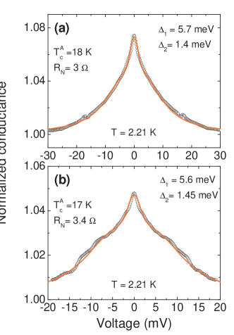
We thus modeled the FS with one hyperboloid (for the electronlike sheets) and one spheroid (for the holelike pocket) as in Fig. 1(d) and assumed an isotropic large gap on the former and an anisotropic small gap on the latter. This gap should represent an evolution of that depicted in Refs. suzuki11 and graser10 when the relevant FS sheet becomes a closed surface. One possibility is to use a -wave gap as in Ref. gonnelli12 , to reproduce the sign change of the OP. However, the symmetry of the OP of Refs. suzuki11 and graser10 in the plane is different from the -wave one and features two additional axes of equation like the one vanharlingen . As a consequence, the probability of constructive interference between electronlike and holelike quasiparticles (that gives rise to the zero-bias peak) is strongly reduced. However, the zero-bias maximum could also arise from the existence of angular regions where the gap has very small amplitude, rather than from its change of sign, as shown in Ref. daghero11 . To account for this possibility, here we modeled the gap on the holelike pockets with a fully anisotropic -wave gap of equation (gridded surface in Fig. 1(d)). The fit of the experimental curves is shown in Fig. 3 (solid lines). The parameters of these two particular fits are listed in the caption. From different fits we get the following average values for the gaps: meV and meV. If one chooses a -wave symmetry for the small gap, a fit of comparable quality is obtained but the values of the gaps are meV and meV gonnelli12 .
IV.3 Ba(Fe1-xCox)2As2 films
Two examples of PCAR spectra in films are shown in Fig. 4. The spectrum in (a) refers to a film on MgO substrate with Fe buffer layer, and shows double-gap features similar to those of Fig. 2(b) but even clearer. The spectrum of panel (b) was measured in a film on CaF2 and presents much smoother structures. In particular, the large gap manifests itself in very broad shoulders at about meV. As stated in a previous section, the normalization in this case gives rise to some ambiguity since the normal state at is not related to the contact alone, but includes a contribution from the portion of the film between the point contact and the voltage electrode. The normalization by a guess normal state can be used, but one should keep in mind that the choice of the presumed normal state can affect the shape of the curve and, to some extent, the fitting parameters – actually, the broadening and the barrier parameter are the most affected by that choice while the values of the gaps are rather robust. The dashed lines in Fig. 4 represent the results of the 3D BTK fit using the same model FS as in Fig. 1(a).
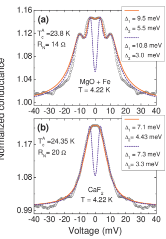
The 3D model is clearly unable to fit the curve very well because of a -enhancing effect due to the shape of the FS daghero11 . The parameters of the fit shown in Fig. 4(a) are meV, meV, , meV, meV, . The weights of the bands, which are not adjustable within this model, are and . Similarly, in Fig. 4(b) the 3D BTK fit (dashed curve) was obtained by using meV, meV, , meV, meV, . Note that in both cases a very deep zero-bias minimum is obtained despite the fact that the intrinsic barrier strength is put equal to zero in band and is very small in band . The failure of the 3D BTK model may be due to different factors. One possibility is that, for some reasons, the probe current is injected mainly along the plane despite the orientation of the film. This may happen, for example, when the surface is rough, a minority percentage of grains are not oriented or the point contact is made by using a sharp tip that may pierce the surface. In our case, all these possibilities are rather unlikely. The other possibility is that the use of two isotropic gaps is not the best choice to reproduce the real distribution of the gaps over the FS. Indeed, the presence of “hot spots” where the gap is significantly suppressed has been evidenced by Raman spectroscopy muschler09 and then justified theoretically mazin10 . Since the hot spots seem to reside on the electronlike FS sheets, one might try to improve the model by using a small anisotropic gap with zeros and a large isotropic gap (as we did in the case of ). This would certainly improve the fit because there would be quasiparticle excitations even at very low energy and the Z-enhancing effect might be compensated by the zero-bias maximum due to these excitations daghero11 . We will explore this possibility elsewhere. For the time being, we show in Fig. 4 what would be the result of a 2D-BTK fit (solid lines). The fit is rather good in the energy region of the gaps and catches the main features of the curves, but just because the weights of the bands were taken to be different from those determined by the shape of the FS in the 3D fit. In (a) we got meV and meV by using and . Of course, changing the weight affects all the fitting parameters: the resulting gap values (averaged over different fits) are meV and meV. The uncertainty is small because the peaks are rather sharp. In (b) we obtained meV and meV, with the weights . Averaging over different fits obtained by changing the weight, the gap values turn out to be meV and . Note that the 2D-BTK fit of similar curves (with current injection along the axis) in single crystals of the same material gave meV and meV tortello10 . There is thus a partial superposition of the gap values, although not a perfect agreement. This is not particularly surprising since: i) there may be some effect of the substrate, especially in the case of the films on Fe buffer layer; ii) the measurements in films highlight a certain degree of inhomogeneity in the superconducting properties, although the film itself is of very high quality; iii) the statistics of the measurements in films needs to be extended to draw definite conclusions.
V Conclusions
We have presented the results of PCAR experiments in single crystals and films with and in single crystals with . The results of these measurements have been analyzed by using a novel 3D version of the BTK model that accounts for the shape of the FS – actually using an analytical model for the real FS calculated within DFT. The results indicate that the two systems, although belonging to the same 122 family of Fe-based compounds, show major differences in the shape of the spectra, and this is a symptom of a difference in the symmetry of the order parameters. In a zero-bias peak or maximum is always observed and can be explained as being due to a strong anisotropy of the smaller gap. DFT calculations show that, at 8% Co content, the holelike FS sheet undergoes a topological transition and splits into separated closed pockets. This can be interpreted as an extreme consequence of the increasing-with-doping warping of this FS sheet, which is predicted to be accompanied by the emergence of 3D nodes in the relevant gap. Indeed, a fit of the spectra is possible by assuming either a -wave gonnelli12 or an anisotropic symmetry of the small gap, to mimic the possible evolution of these 3D nodes when the topological transition occurs. In the case of at , the calculated FS shows markedly warped holelike sheets but no topological transitions. The spectra taken in single crystals with the current injected along the plane can be fitted with two isotropic gaps; the agreement between model and data is limited to the central region of the spectra because of additional structures around 20 meV that are due to the strong electron-boson coupling tortello10 ; daghero11 and cannot be reproduced within this approach. Instead, the fit of the -axis spectra measured in thin films with the same model is unsuccessful around zero bias, where the so-called -enhancing effect due to the shape of the FS produces a strong depression of the conductance which is not observed experimentally. This might be the sign of the presence of gap minima mazin10 whose existence has been inferred from Raman spectroscopy results muschler09 .
Acknowledgments
This work was done under the Collaborative EU-Japan Project “IRON SEA” (NMP3-SL-2011-283141) and under the PRIN Project No. 2008XWLWF9-005 of the Italian Ministry of Research.
References
- (1) Y. Kamihara, T. Watanabe, M. Hirano, and H. Hosono. J. Am. Chem. Soc., 130:3296, 2008.
- (2) I. I. Mazin, D. J. Singh, M. D. Johannes, and M. H. Du. Phys. Rev. Lett., 101:057003, 2008.
- (3) I. I. Mazin. Nature, 464:183, 2010.
- (4) J. Paglione and R. L. Greene. Nature Phys., 6:645–58, 2010.
- (5) I. I. Mazin, T. P. Devereaux, R. Hackl, B. Muschler, J. G. Analytis, Jiun-Haw Chu, and I. R. Fisher. Phys. Rev. B, 82:180502(R), 2010.
- (6) K. Kuroki, H. Usui, S. Onari, R. Arita, and H. Aoki. Phys. Rev. B, 79:224511, 2009.
- (7) K. Suzuki, H. Usui, and K. Kuroki. J. Phys. Soc. Jpn., 80:013710, 2011.
- (8) K. Terashima, J. H. Bowen, K. Nakayama, T. Sato, P. Richard, Y.-M. Xu, L. J. Li, G. H. Cao, Z.-A. Xu, H. Ding, and T. Takahashi. Proc. Natl. Acad. Sci (USA), 106:7330, 2009.
- (9) R. S. Gonnelli, M. Tortello, D. Daghero, R. K. Kremer, Z. Bukovski, N. D. Zhigadlo, and J. Karpinski. Supercond. Sci. Technol., 25:065007, 2012.
- (10) B. Muschler, W. Prestel, R. Hackl, T. P. Devereaux, J. G. Analytis, J.-H. Chu, and I. R. Fisher. Phys. Rev. B, 80:180510(R), 2009.
- (11) A. S. Sefat, R. Jin, M. A. McGuire, B. C. Sales, D. J. Singh, and D. Mandrus. Phys. Rev. Lett., 101:117004, 2008.
- (12) M. Matusiak, Z. Bukowski, and J. Karpinski. Phys. Rev. B, 81:020510(R), 2010.
- (13) L. Harnagea, S. Singh, G. Friemel, N. Leps, D. Bombor, M. Abdel-Hafiez, A. U. B. Wolter, C. Hess, R. Klingeler, G. Behr, S. Wurmehl, and B. B uchner. Phys. Rev. B, 83:094523, 2011.
- (14) D. Daghero and R.S. Gonnelli. Supercond. Sci. Technol, 23:043001, 2010.
- (15) T. Y. Chen, S. X. Huang, and C. L. Chien. Phys. Rev. B, 81:214444, 2010.
- (16) R. S. Gonnelli, D. Daghero, M. Tortello, G. A. Ummarino, V. A. Stepanov, J. S. Kim, and R. K. Kremer. Phys. Rev. B, 79:184526, 2009.
- (17) D. J. Singh. Phys. Rev. B, 78:094511, 2008.
- (18) R. Hu, S. Ran, S.L. Bud’ko, W. E. Straszheim, and P. C. Canfield. Unpublished, arXiv:1111.7034, Nov 2011.
- (19) N. Colonna, G. Profeta, A. Continenza, and S. Massidda. Phys. Rev. B, 83:094529, 2011.
- (20) R. Mittal, S. K. Mishra, S. L. Chaplot, S. V. Ovsyannikov, E. Greenberg, D. M. Trots, L. Dubrovinsky, Y. Su, Th. Brueckel, S. Matsuishi, H. Hosono, and G. Garbarino. Phys. Rev. B, 83:054503, 2011.
- (21) M. Tortello, D. Daghero, G. A. Ummarino, V. A. Stepanov, J. Jiang, J. D. Weiss, E. E. Hellstrom, and R. S. Gonnelli. Phys. Rev. Lett., 105:237002, 2010.
- (22) D. Daghero, M. Tortello, G.A. Ummarino, and R. S. Gonnelli. Rep. Prog. Phys., 74:124509, 2011.
- (23) S. Graser, A. F. Kemper, T. A. Maier, H.-P. Cheng, P. J. Hirschfeld, and D. J. Scalapino. Phys. Rev. B, 81:21450, 2010.
- (24) D. J. Van Harlingen. Rev. Mod. Phys, 67:515–37, 1995.