Enhanced Efficiency of Light-Trapping Nanoantenna Arrays for Thin Film Solar Cells
Abstract
We suggest a novel concept of efficient light-trapping structures for thin-film solar cells based on arrays of planar nanoantennas operating far from plasmonic resonances. The operation principle of our structures relies on the excitation of chessboard-like collective modes of the nanoantenna arrays with the field localized between the neighboring metal elements. We demonstrated theoretically substantial enhancement of solar-cell short-circuit current by the designed light-trapping structure in the whole spectrum range of the solar-cell operation compared to conventional structures employing anti-reflecting coating. Our approach provides a general background for a design of different types of efficient broadband light-trapping structures for thin-film solar-cell technologically compatible with large-area thin-film fabrication techniques.
Keywords: thin-film solar cell, light-trapping structure, nanobar, trapezoidal nanoantenna, domino mode
I Introduction
The extensive study of thin-film solar cells (TFSC) aims for the production of large-area panels harvesting the solar energy. Prospective TFSC imply their implementation on flexible substrates compatible with the so-called roll-to-roll processing nanosolar . Such solar cells are characterized by a very small amount of purified semiconductor per unit area SC1 which reduces the cost being useful for ecology SC1 ; SC2 .
To make efficient solar cells of a very small thickness, an anti-reflecting coating should be replaced by a light-trapping structure, since none of the conventional anti-reflecting coatings can prevent the transmission of light through a photovoltaic layer. This transmission results in energy loss and substrate heating, which lead to an additional reduction of the solar cell efficiency SC1 ; SC2 . A light-trapping structure (LTS) is a structure capable to reduce both the reflection from a solar cell and transmission through its photo-absorbing layer.
Many suggestions for a LTS design are based on photonic crystals (e.g., Refs. SC3 ; SC4 ; SC5 ), nano-textured semiconductor coatings (e.g., Refs. SC6 ; SC7 ; SC8 ), and plasmonic nanostructures (e.g., Refs. SC9 ; SC10 ; SC11 ). Some LTSs performed as regular plasmonic gratings SC11 ; SC12 ; Spinelli operate similarly to the semiconductor textured coatings, i.e. they convert incident plane waves into waveguide modes propagating inside the photovoltaic layer. The operation of textured coatings obeys certain basic restrictions SC12 ; SC13 ; SC14 known as the Yablonovich limit. It relates the field confinement inside a semiconductor slab with the maximal operation band and minimal optical thickness of the slab. This limit, however, refers to the ray optics, and in the case of plasmonic gratings it can be overcame by involving surface plasmon polaritons SC12 ; Spinelli ; SC20 .
Many ideas of the efficient light trapping for TFSC are based on the use of plasmonic absorbers SC13 ; SC14 ; SC9 ; SC10 ; SC11 which are planar arrays of silver or gold nanoparticles with plasmon resonances within the operation band of solar cells. Plasmonic absorbers can be divided into two classes. The first class is random arrays of nanoparticles where only averaged parameters (averaged size of the particles and their surface density) are optimized. Such structures are fabricated by self-assembly, and they have the geometry close to that of a pillar or a tablet. These plasmonic absorbers can be engineered so that at certain frequencies both reflection from the solar cell and transmission through the photovoltaic layer are strongly suppressed SC14 ; SC9 ; SC10 ; SC11 . From a macroscopic point of view, such an absorber can be treated as an effective lossy layer with a broadband resonance of the complex permittivity. The general drawback of these absorbers are high losses in metal nanoparticles and noticeable scattering.
The second class of plasmonic absorbers is regular grids of silver or gold nanoparticles located on a top of traditional vertical p-n or p-i-n junctions (e.g., Refs. SC15 ; SC16 ; SC17 ; SC18 ). We call such structures arrays of nanoantennas. Such nanoantenna arrays can demonstrate several plasmon resonances SC15 ; SC18 , and they can operate even as dielectric optical cavities SC19 . Nanoantennas not only offer a significant enhancement of the photovoltaic absorption, but they can concentrate the field outside the metal elements avoiding useless dissipation of the solar energy.
In this paper, we suggest and study theoretically a novel type of light-trapping structures based on arrays of nanoantennas excited far from plasmonic resonances. We demonstrate that such non-resonant absorbers can enhance substantially the photoabsorption in very thin (100-150 nm) semiconductor layers and increase significantly the overall spectral efficiency of solar cells with a very small thickness of an active layer. Our LTS are in-plane optically isotropic (being also independent on the light polarization) coatings located on the top of a solar cell. We discuss possible implementations of our concept in the solar cell technology and analyze in detail two specific examples of TFSC: inter-band TFSC based on copper-indium-gallium-selenide (CIGS) and silicon TFSC.
II Physics of enhanced light trapping
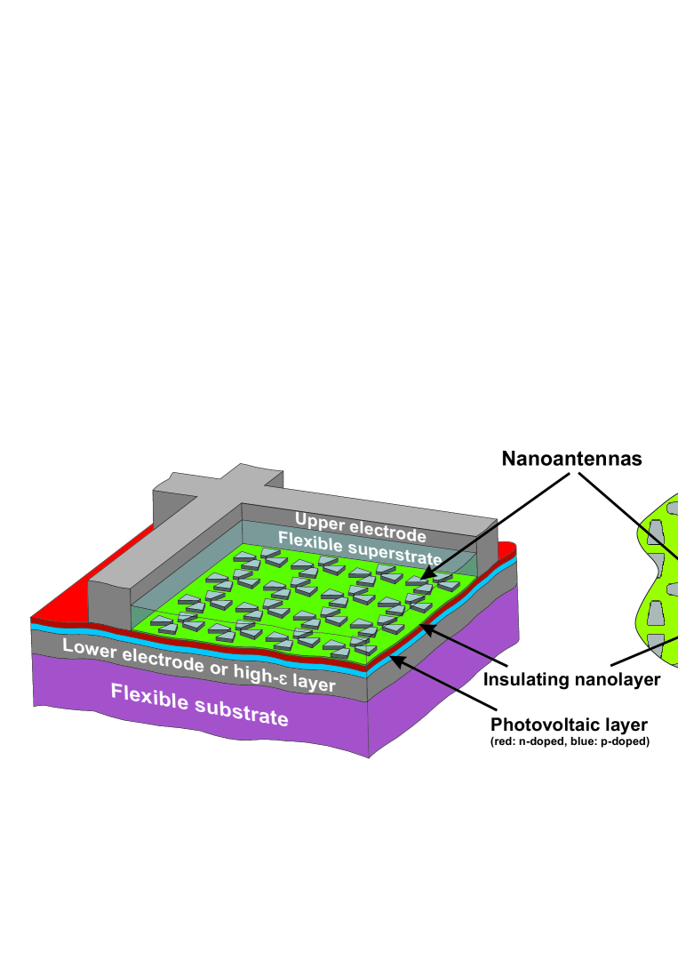
A schematic view of our LTS is shown in Fig. 1. This design employs the advantages of collective oscillations excited in the visible or infrared spectral range by an incident plane wave in a lattice of Ag nanobar nanoantennas. The chessboard-like modes in our structure are analogous to the collective oscillations discussed in Ref. domino for arrays of parallel metal bar operating in the far-infrared range and termed domino modes. Such modes exist are excited at several wavelengths by the external electric field whose vector is orthogonal to the bar axis, and they are characterized by the domination of higher multipole moments induced in every nanobar over its dipole moment. The main feature of such modes is the advantageous distribution of the local electric field which is concentrated in the gaps between the nanobars. The internal field in metal is small, and consequently these modes demonstrate low losses. The chessboard-like modes can be excited also in the visible range Olli if the thickness of the bar is within 50-100 nm and its length is larger than 200-250 nm.
In several earlier studies domino ; Olli , these modes were excited by an incoming beam with the grazing incidence on the array plane. However, our simulations reveal that these modes are also excited for any angle of incidence (e.g. by a normally incident wave) as well as in the presence of a substrate or without any substrate.
When these modes are excited in arrays of nanobar nanoantennas located in free space Olli , the absorption maxima at the wavelength of these modes are weak. Their excitation implies the electromagnetic energy is stored between the nanobars without an impact on reflectance and transmittance. This situation changes dramatically if the nanobars are located in the absorbing host or on an absorbing substrate. Then the electromagnetic energy of the near-field concentrated in between the nanobars is absorbed by a host medium. In this way both reflection and transmission of the incident wave can be suppressed at several wavelengths.
The presence of a substrate leads to a change of the bar cross section compared to that discussed in Ref. Olli . For arrays of nanobars located on a semiconductor substrate, the domino modes correspond to a rectangular cross section, whereas the bar thickness should be 2-3 times as smaller as the width. In our simulations the parallel nanobars located on a-Si substrate have the thickness 40-70 nm, width 100-150 nm, and length 200-500 nm. These domino modes are excited at several wavelengths in the visible range, and their total band has a relative width close to 20%. The further enlargement of the band became possible by employing tapering of nanobars. This design allows overlapping of separate wavelength ranges of the domino modes which form a solid band with a relative width 40-50%. This band is still narrower than the operational band of a practical solar cell, and nanobars of LTS should not worsen the operation of the solar cell beyond the band of the light trapping. This means that the arrays of tapered nanobars should be sparse enough to prevent strong reflection from metal elements.
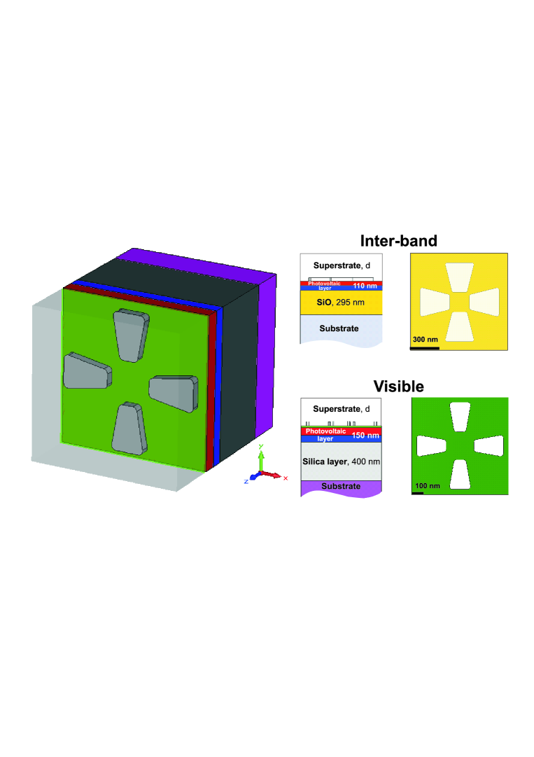
Next, in order to achieve the polarization-independent response, our LTS should comprise of at least two orthogonal arrays of light-trapping nanobars. Two latter requirements result in a unit cell performed as a cross of tapered nanobars. The unit cell shown in Fig. 2 operates as a broadband polarization-independent nanoantenna. However, light trapping in the arrays is a collective effect which disappears when the gap between the adjacent nanoantennas becomes too large.
The underlying physical mechanism of light trapping due to the excitation of low-loss chessboard-like domino modes can be complemented by the effect of the Fabry-Perot cavity which can be engineered in the adjacent frequency range. We managed to achieve this regime in our numerical simulations for the case when an additional dielectric layer of high permittivity (of the order of 3-4) is introduced between the substrate and photovoltaic layer. For the substrate of amorphous silicon, it can be a layer of silicon monoxide. Then, in a desired frequency range, the whole structure creates a Fabry-Perot cavity with both small transmission and small reflection of incident waves.
III Suggested design and numerical results
We calculate numerically the power absorbed by a unit cell of the TFSC structure with LTS within the operation band of the photovoltaic layer. The power absorbed in the photovoltaic layer is defined as an integral of the local power density over the volume of the layer per unit cell, and the power absorbed in the nanoantenna is defined as the integral over the volume of metal per unit cell. In both the cases, the local electric field is calculated for the normally incident plane wave with the unit amplitude of the electric field. Our calculations are performed for two cases: The first case is LTS and a blooming layer, the latter is a simplest type of ARC, and it is used for comparison. Though anti-reflecting properties of multilayer anti-reflection coating are slightly better, they are achieved by a nanometer precision being more sensitive to nanometer variations of the thickness than the reflectance of a single blooming layer Shalin1 ; Shalin2 . As a result, the optical properties of a multilayer ARC suffer of abrasion more than those of a simple ARC. Therefore, we compare the short-circuit current of a TFSC calculated in the presence of our LTS and that of a single dielectric layer whose permittivity and thickness are optimized for minimizing the reflection.
Our numerical simulations are carried out using both Ansoft HFSS and CST Studio software packages. The meshing is refined so that the result would not depend on the computational grid, and the convergence is carefully controlled. The agreement between the results obtained with the HFSS and CST Studio packages is excellent: the plots presented below visually coincide. Moreover, we employ two options of the Ansoft HFSS package – an incident plane wave and a wave port – and obtained the same coincidence. The unit cell of the LTS shown in Fig. 2 refers to the TFSC region located in the gaps between the wires of the electrodes collecting the photo current. These mesh electrodes should be located on both top and bottom of the photovoltaic layer. We do not consider the regions shaded by the wire mesh assuming that they are much smaller than the regions open to the sunlight.
First, we show that the gain in the short-circuit current due to the presence of the LTS equals to the gain in the absorption of the incident wave with uniform spectrum in the photovoltaic layer. This absorption should be averaged over the operation band of the solar cell with a certain weight function as determined below. The short-circuit current per unit area of the solar cell is equal to (see e.g. SC10 ; SC15 ):
| (1) |
Here is the spectral response of the photovoltaic material whose complex permittivity has the imaginary part , and is the electric field produced by the solar radiation inside the photovoltaic layer. Since the problem is linear, the field can be expressed through the solar irradiance as , where is the field produced by the incident wave of unit amplitude at every frequency. Then we can write , where
| (2) |
is the spectral photo-absorption of the wave with unit amplitude. We can further express the value in the form:
| (3) |
Here is the spectral absorption averaged over the band with the weight function which is a product of two table values (photovoltaic spectral response of the photovoltaic material layer and the spectrum of solar irradiance at the earth surface). To calculate the short-circuit current, we simulate the wave absorption with an unit amplitude over the band , and then average it with the weight function . After calculating for the case when the TFSC is covered by LTS and the case when it is covered by a dielectric ARC, we obtain the gain due to the replacement of the ARC by LTS:
| (4) |
The first photovoltaic structure for which we perform the optimization of the nanoantenna arrays is a 110-nm thick n-p layer of CuInSe2 located between a polyethylene superstrate and a layer of silicon monoxide. This kind of CIGS (when Ga is fully substituted by In) corresponds to a solar cell with photovoltaic spectral response and optical losses essentially overlapping in the inter-band region 250-450 THz CIGS0 ; CIGS1 . The thickness of the CuInSe2 layer is chosen as small as 110 nm in order to stress the light-trapping capacity of our LTS. From other point, this thickness is larger than the depletion region around the p-n junction and smaller than the minimum carrier diffusion length CIGS_L ; CIGS_L1 . Therefore, the selected thickness of the photovoltaic layer corresponds to a ratio between the photo-current and photo-absorption SC2 . In this regime, the increase of the photovoltaic absorption has the maximal possible impact on the overall efficiency of the solar cell.
The optical constants of doped CuInSe2 are taken from Ref. CIGS , and the optical constants of polyethylene are taken from Ref. Polyethilene , for the region 400-450 THz, and Ref. Polyethilene_IR , for the region 250-400 THz. Those of the silicon monoxide are taken from Ref. silica . The optimal thickness of the polyethylene layer is 270 nm whereas it is 295 nm for SiO. Other parameters are shown in Fig. 2.
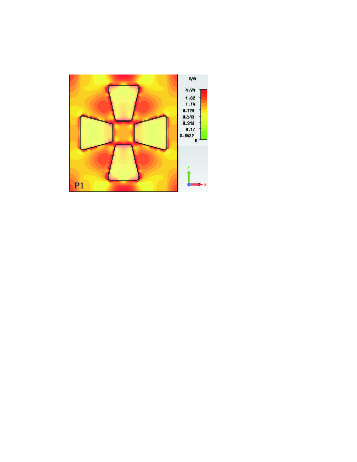
Within the frequency range 350-450 THz, the light is trapped by nanoantenna arrays where the chessboard-like domino modes are excited. This is seen from the local field distributions over the unit cell at these frequencies. In Figs. 3(a,b), we show the local field distribution at the frequency 370 THz in the central vertical cross section of the unit cell and in the horizontal plane P1 – upper surface of the insulating layer of amorphous silica separating nanoantennas from the semiconductor. We vary its thickness within the range 2-20 nm and find that its presence affects none of the main characteristics, such as absorption in the semiconductor and metal elements, and the coefficients and . In Fig. 3(a) we observe a rather strong reflected field. Due to the presence of nanoantennas, the reflectance increases nearly by 30%. However, the decrease of the transmittance is more important, and the light-trapping effect is quite significant. Inspecting the field distribution in Fig. 2(a), we observe a practical absence of the transmitted field. In both the cases shown in Figs. 2(a,b) we find that the field is concentrated beyond the metal elements, and the harmful dissipation of the solar power inside the LTS is thus prevented.
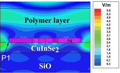
Location of the local field maxima in Fig. 2 outside the photovoltaic layer (mainly in the dielectric superstrate) is not a drawback of our LTS design. To maximize the photo-absorption, it is not mandatory to concentrate the field inside the photovoltaic layer. Evanescent field concentrated in the dielectric superstrate is neither absorbed or nor radiated. The absorption occurs only in those parts of hot spots which are located inside the metal and semiconductor. It is important that the useful absorption in the semiconductor exceeds strongly the harmful absorption in the metal.
In the frequency range 250-350 THz, the nanoantennas are weakly excited and the light-trapping occurs due to the regime of the Fabry-Perot cavity. In Fig. 4, we show the spectral photo-absorption for three cases: with our LTS, with a blooming layer, and without any structure on the top of the photovoltaic layer. The optimal blooming is achieved using the same polyethylene film with the thickness 440 nm. We notice that the refraction index of the polyethylene corresponds approximately to the blooming condition for the half-space of CIGS over a significant part of the operation band.
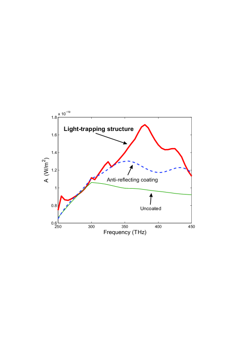
The reflection losses averaged over the operation frequency band in the presence of LTS are found to be close to 20%, averaged transmission losses are about 8%, while only 6% of the incident power is absorbed in the LTS nanoantenna arrays. This gives us an useful absorption about 66% of the incident power. with the presence of ARC, the reflection losses are 7% and transmission losses are as large as 46%. IN this later case the absorption equals 49% (cf. with 38% in the non-coated case). The gain due to the LTS is estimated as 1.34 compared to the case of ARC. Using formula (LABEL:eq:gain), we obtain 1.29 due to the presence of the weight function in the averaged absorption . Compared to the non-coated cell, the LTS gives the gain of 1.7.
We believe that the obtained enhancement is sufficient to justify the fabrication costs of our LTS nanoantennas. Below, we discuss the possibility to fabricate our LTS in a way which seems to be rather inexpensive under the condition of the mass production and compatibility with the roll-to-roll processing nanosolar .
Our second numerical example of LTS corresponds to the silicon solar cell whose operation band is practically coincide with the range of the visible light. The study of the second design aims to demonstrate that our design concept allows different types of TFSC operating in different frequency bands. For this latter case, the dimensions shown in Fig. 2 are numerically optimized for the photo-absorbing layer of the thickness 150 nm. The density of carriers in the layer is assumed to be cm-3. The dielectric superstrate is amorphous silica as well as the ARC in the reference solar cell. The simplistic blooming condition does not provide a good estimate for a multi-layer structure with a high optical contrast of layers. A silica film with the thickness 175 nm reduces the reflection averaged over the visible range almost 5 times (from 45% to 10%) enhancing the averaged absorption by 40%.
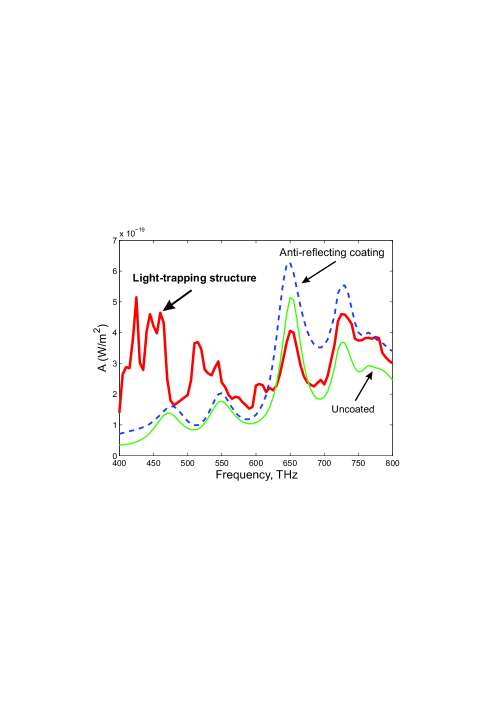
In Fig. 5, we show the frequency dependence of the photovoltaic absorption for three three cases discussed above: (i) optimal LTS, (ii) optimal blooming layer, and (iii) non-coated solar cell. The best superstrate thickness for our LTS is equal to 325 nm, however we find that the absorption depends weakly on the thickness in the interval 325-390 nm, and the nanometer precision is not required. In the presence of nanoantennas, the light-trapping effect related to the domino modes is observed in the region 400-600 THz. At 600-800 THz the nanoantennas are weakly excited and only slightly worsen the blooming operation of the silica superstrate. The gain in the photovoltaic absorption calculated in accord with Eq. (LABEL:eq:f2) is 17% (). Compared to the non-coated TFSC, our LTS gives the gain 64%. These results are close to those obtained for the CIGS solar cells.
Choosing the best material for nanoantennas, we study different metals and find that only silver can properly satisfy the light-trapping functionality. With other metals the domino modes are not found. We believe that for other metals either absolute value of the complex permittivity is not sufficiently large (Au) or optical losses are too high (Cr, Al, Cu).
IV Fabrication issues
Now we discuss briefly possible technologies for the fabrication of suggested arrays of nanoantennas with a dielectric superstrate in a way compatible with the roll-to-roll processing nanosolar for large-area TFSC panels. First, we suggest to fabricate the arrays of nanoantennas on a polymer film using the replication technology Novac the latter implies a quartz template whose surface repeats the profile of the nanoantenna arrays. Using the method described in Ref. Novac with this template, one can obtain a vast amount of plastic replicas with metal nanoantennas reproduced with practically the same resolution as that of the template. Besides polyethylene, these plastic substrates can be made of polyamide, polymethylmetaacrylate, polytetrafluorethylene, polystyrene, etc. Pieces of the film (of size 0.5-1 mm) with printed nanoantenna arrays can be prepared separately from solar cells so that the price of every piece will be small. Then these pieces can be placed on the top of the solar cell in the gaps between the wires of the mesh electrode. If it is done in a vacuum camera and under mechanical pressure, a strong bonding arises between the polymer and the silica covering the surface of the solar cell. In accord to our estimates, this bonding would be sufficient for adhesion, and the nanoantennas will be fixed on the solar cells as well as the plastic superstrate. Finally, the thickness of the superstrate can be reduced chemically to a few submicrons. This procedure is feasible if the gaps between the wires of the contact mesh are as large as 0.5-1 mm which are typical values for known mesh electrodes of TFSC structures Meier .
Alternatively, our structures can be fabricated by using conducting polymers anodes or any other flexible transparent electrode. Then the nanoantennas can be fabricated on the top of a solar cell protected by a silica insulator being covered by a flexible conducting coating. This coating will play twofold role: as an upper electrode and also a superstrate of our light-trapping structure. To prevent an ohmic contact with the superstrate, the nanoantenna arrays can be covered with organic molecules or a nanolayer of deposited silica. In the gaps between nanoantennas, the silica insulator should be removed from the surface of the photovoltaic layer. In both the cases our design is compatible with the concept of the roll-to-roll processing of thin-film solar cells.
V Conclusions
We have suggested and analyzed theoretically a novel design of light-trapping solar-cell nanopatterned structures which allows a significant enhancement of the photovoltaic absorption in the layers as thin as 110 nm. Our design is material-independent, and it can be applied to a variety of solar cells operating in the visible, inter-band or infrared frequency range. More importantly, the light-trapping functionality of our structures is broadband, and it is not based on spectrally narrow plasmonic or any other resonances. Light trapping in the structures originates from the excitation of chessboard-like modes (also called domino modes) of a lattice of tapered silver nanobar nanoantennas which can be excited for different geometric parameters within a vast frequency spectrum ranging from far-IR to the visible. We have demonstrated that our nanoantenna arrays operate significantly better than the structures based on anti-reflecting coatings. We have discussed the design issues with respect to possible mass-fabrication of our nanoantennas.
VI Acknowledgements
This work has been supported by the Ministry of Education and Science of Russian Federation, the Dynasty Foundation and the Australian Research Council. The authors thank K.R. Catchpole and H. Savin for useful discussions and suggestions.
References
-
(1)
Ultra-Low-Cost Solar Electricity Cells, An Overview of Nanosolar s
Cell Technology Platform, Nanosolar, Inc.
White Paper - September 2, 2009, available at
www.catharinafonds.nl/wp-content/uploads/2010/03/NanosolarCellWhitePaper.pdf - (2) A. Marti and A. Luque, Next-generation photovoltaics, Institute of Physics Publishing, Bristole-Philadelphia, 2004
- (3) J. Nelson, The Physics of Solar Cells, Imperial College Press, 2003.
- (4) C. Heine and H. M. Rudolf, Submicrometer gratings for solar energy applications, Appl. Opt. 34(14), 2476 (1995).
- (5) P. Bermel, C. Luo, L. Zeng, L. C. Kimerling, and J. D. Joannopoulos, Improving thin-film crystalline silicon solar cell efficiencies with photonic crystals, Opt. Express 15(25), 16986 (2007).
- (6) S. B. Mallick, M. Agrawal, and P. Peumans, Optimal light trapping in ultra-thin photonic crystal crystalline silicon solar cells, Opt. Express 18(6), 5691 (2007).
- (7) P. Campbell and M. A. Green, Light trapping properties of pyramidally textured surfaces, J. Appl. Phys. 62, 243 (1987).
- (8) R. Brendel, Thin-Film Crystalline Silicon Solar Cells: Physics and Technology, Wiley-VCH, 2003.
- (9) L. Zeng, Y. Yi, C. Hong, J. Liu, N. Feng, X. Duan, L. C. Kimerling, and B. A. Alamariu, Effciency enhancement in Si solar cells by textured photonic crystal back reflector, Appl. Phys. Lett. 89, 111 (2006).
- (10) H. W. Deckman, C. R. Wronski, H. Witzke, and E. Yablonovitch, Optically enhanced amorphous silicon solar cells, Appl. Phys. Lett. 42, 968 (1983).
- (11) J. Müller, B. Rech, J. Springer, and M. Vanecek, TCO and light trapping in silicon thin-film solar cells, Solar Energy 77(6), 917 (2004).
- (12) K.R. Catchpole, A. Polman, Plasmon-enhanced solar cells, Appl. Phys. Lett. 93 191113 (2008).
- (13) Yu.A. Akimov, K. Ostrikov, E. P. Li, Surface Plasmon Enhancement of Optical Absorption in Thin-Film Silicon Solar Cells, Plasmonics, 4 107 (2009).
- (14) H. A. Atwater and A. Polman, Plasmonics for improved photovoltaic devices, Nature Mat. 9, 205 (2010).
- (15) E. Yablonovitch and G. D. Cody, Intensity enhancement in textured optical sheets for solar cells, IEEE Trans. Electron. Dev. 29(2), 300 (1982).
- (16) P A Spinelli, V E Ferry, J van de Groep, M van Lare, M A Verschuuren, R E I Schropp, H A Atwater and A Polman, Plasmonic light trapping in thin-film Si solar cells, J. Optics 14, 024002 (2012).
- (17) D.M. Callahan, J.N. Munday, and H.A. Atwater, Solar cell light trapping beyond the ray optic limit, Nano Lett. 12, 214 (2011).
- (18) R.A. Pala, J. White, E. Barnard, J. Liu, and M.L. Brongersma, Design of Plasmonic Thin-Film Solar Cells with Broadband Absorption Enhancements, Adv. Mater., 21, 1 (2009).
- (19) C. Rockstuhl and F. Lederer, Photon management by metal nanodisks in thin-film solar cells, Appl. Phys. lett. 94, 213102 (2009).
- (20) Y. Wang, T. Sun, T. Paudel, Y. Zhang, Zh. Ren, and K. Kempa, Metamaterial-Plasmonic Absorber Structure for High Efficiency Amorphous Silicon Solar Cells, Nano Lett. 12, 440 (2012).
- (21) V.E. Ferry, L.A. Sweatlock, D. Pacifici, and H.A. Atwater, Plasmonic Nanostructure Design for Efficient Light Coupling into Solar Cells, Nano Lett., 8(12), 4391 (2008).
- (22) J. Grandidier, D.M. Callahan , J.N. Munday, and H.A. Atwater, Light Absorption Enhancement in Thin-Film Solar Cells Using Whispering Gallery Modes in Dielectric Nanospheres, Adv. Mater. 23, 1272 (2011)
- (23) D. Martin-Cano, M. L. Nesterov, A. I. Fernandez-Dominguez, F. J. Garcia-Vidal, L. Martin-Moreno, E. Moreno, Domino plasmons for subwavelength terahertz circuitry, Optics Express 18, 754 (2010).
- (24) C. Simovski and O. Luukkonen, Tapered plasmonic waveguides with efficient and broadband field transmission, Opt. Comm. 285, 3397 (2012).
- (25) S. Walheim, E. Schaffer, J. Mlynek, and U. Steiner, Closely packed and aspect-ratio-controlled antireflection subwavelength gratings on GaAs using a lenslike shape transfer, Science 283, 520 (1999).
- (26) A.S. Shalin, Optical blooming of a medium by nanocrystal layers, Quantum Electronic 41, 163 (2011).
- (27) G. Brown, V. Faifer, A. Pudov, S. Anikeev, E. Bykov, M. Contreras, and J. Wu, Determination of the minority carrier diffusion length in compositionally graded Cu(In,Ga)Se2 solar cells using electron beam induced current, Appl. Phys. Lett. 96, 022104 (2010).
- (28) A. Goetzberger, C. Hebling, and H.-W. Schock, Photovoltaic materials, history, status and outlook, Materials Science and Engineering R R40, 1 (2003).
- (29) T.Negami, S. Nishiwaki, Y. Hashimoto, and N. Kohara, Effect of the absorber thickness on performance of Cu(In,Ga)Se2 solar cells, Proceedings of the 2nd World Conference on Photovoltaic Energy Conversion, Vienna, Austria, May 12-15, 1998; pp. 1181 1184.
- (30) P.D. Paulson, R.W. Birkmire, and W.N. Shafarman, High-efficiency solar cells based on Cu(InAl)Se2 thin films, J. Appl. Phys., 879, 94 (2003).
- (31) M.I. Alonso, M. Carriga, C.A. Durante-Rincon, E. Hernandez, and M. Leon, Optical functions of chalcopyrite CuGaxIn1-xSe alloys, Appl. Phys. A 74, 659 (2002).
- (32) Database of Thin Films, available at http://www.filmetrics.com/refractive-index-database/Polyethylene/PE-Polyethene
- (33) S. N. Kasarova, N. G. Sultanova, C. D. Ivanov, I. D. Nikolov, Analysis of the dispersion of optical plastic materials, Optical Materials 29, 1481 (2007).
- (34) J. W. Horwitz, Infrared refractive index of polyethylene and a polyethylene-based material, Optical Engineering 50(9), 093603 (2011).
- (35) G. Hass and C. Salzberg, Optical Properties of Silicon Monoxide in the Wavelength Region from 0.24 to 14.0 Microns, JOSA 44(3), 181 (1954)
- (36) N. Tajik, Z. Peng, P. Kuyanov and R.R. LaPierre, Sulfur passivation and contact methods for GaAs nanowire solar cells, Nanotechnology 22 (2011) 225402.
- (37) A. S. Ferlauto, G. M. Ferreira, J. M. Pearce, C. R. Wronski, R. W. Collins, X. Deng, and G. Ganguly, Analytical model for the optical functions of amorphous semiconductors from the near-infrared to ultraviolet, J. Applied Phys. 92, 2424 (2002).
- (38) J. Meier, J. Spitznagel, U. Kroll, C. Bucher, S. Fay, T. Moriarty, and A. Shah, Potential of amorphous and microcrystalline silicon solar cells, Thin Solid Films 451-452, 518 (2004).
- (39) D.K. Kotter, S.D. Novack, W.D. Slafer, P. Pinhero, Theory and Manufacturing Processes of Solar Nanoantenna Electromagnetic Collectors, J. Solar Energy Engineering 132, 011014 (2010).
- (40) S.-I. Na, S.-S. Kim, J. Jo, and D.-Yu Kim, Efficient and Flexible ITO-Free Organic Solar Cells Using Highly Conductive Polymer Anodes, Adv. Mat. 20, 4061 (2008).