Electrically tunable transverse magnetic focusing in graphene
Electrons in a periodic lattice can propagate without scattering for macroscopic distances despite the presence of the non-uniform Coulomb potential due to the nuclei Bloch_Blochwave . Such ballistic motion of electrons allows the use of a transverse magnetic field to focus electrons Tsoi_firstMEF . This phenomenon, known as transverse magnetic focusing (TMF), has been used to study the Fermi surface of metals Tsoi_1999 and semiconductor heterostructures Houten_ElectronFocusing , as well as to investigate Andreev reflection Tsoi_1999 , spin-orbit interaction Rokhinson_SpinSeparation , and to detect composite fermions Goldman_DetectionOfCompositeFermions ; Smet_CompositeFermions . Here we report on the experimental observation of transverse magnetic focusing in high mobility mono-, bi-, and tri-layer graphene devices. The ability to tune the graphene carrier density enables us for the first time to investigate TMF continuously from the hole to the electron regime and analyze the resulting “focusing fan”. Moreover, by applying a transverse electric field to tri-layer graphene, we use TMF as a ballistic electron spectroscopy method to investigate controlled changes in the electronic structure of a material. Finally, we demonstrate that TMF survives in graphene up to K, by far the highest temperature reported for any system, opening the door to novel room temperature applications based on electron-optics.

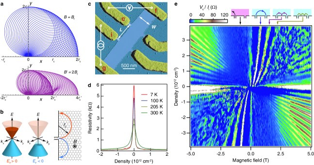
The concept of TMF can be illustrated by considering electrons entering a two-dimensional system through a narrow injector (origin in Fig. 1a). In the presence of a magnetic field , electrons will undergo cyclotron motion with radius and get focused on the caustic (a quarter of a circle with radius ) on which the electron density becomes singular (Fig. 1a, top). Moreover, the specular reflection of electrons at the boundary of the two-dimensional system causes a skipping orbit motion which results in focal points at integer multiples of along the -axis (Fig. 1a, bottom). This basic behavior still holds for electron motion in a solid as long as the Fermi surface has cylindrical symmetry Tsoi_1999 . Hence, the magnetic field, , required to focus electrons at a distance is
| (1) |
where is the number of reflections off the edge of the system (e.g. corresponds to direct injector to collector trajectory, without reflections), is the reduced Planck’s constant, is the elementary charge, is the Fermi momentum, and where we have used , being the carrier density.
In order to study TMF in graphene, we fabricate Hall bar devices based on high mobility mono- (MLG), bi- (BLG), and tri-layer (TLG) graphene on hexagonal boron nitride (hBN) substrates Dean_BN (see Methods and Fig. 1c). The multi-terminal geometry required to study TMF imposes a minimum mean free path of the order of several hundred nm, which has only been possible with the advent of G on hBN devices Dean_BN ; Thiti_tri ; Mayorov_BendResistance . Figure 1d shows the resistivity of a MLG device as a function of density at zero magnetic field. The device exhibits a narrow Dirac peak with a strong temperature dependence, which indicates low disorder Du_Ballistic ; Bolotin_TDependentSusGra . Its field effect mobility is cmVs-1 at low temperature, corresponding to a mean free path of m. A similar behavior is observed for BLG and TLG devices. The high mobility and low disorder enable us to probe TMF in these devices.
We employ the measurement configuration shown in Fig. 1c to probe the focusing of electrons. Current is injected through contact i while contact g is grounded and voltage is measured at the collector (contact c) relative to contact f. The magnetic field is applied normal to graphene. Figure 1e shows the normalized in MLG, at K. Two sets of features are immediately apparent: for T, we observe Shubnikov-de Hass oscillations (SdHOs), forming a usual Landau fan, as expected from the measurement setup, which is topologically equivalent to a longitudinal resistance measurement. While the SdHOs are very pronounced in quadrants 2 and 4 (top-left and bottom-right), they are nearly invisible in quadrants 1 and 3, due to the interference of different trajectories of electrons propagating coherently to the collector Houten_ElectronFocusing ; Beenakker_modeInterference ; Aidala_ImagingFocusing ; Rakyta_ElectronFocusingTheory (see supplementary information).
In the low field regime, T, we observe three unusual peaks which do not resemble SdHOs. For positive density, these peaks appear on the positive side. The location of these features in the plane (see Eq. 1) indicates that these peaks can be associated with TMF. The peaks arise when electrons are focused onto the collector, resulting in a build up of . The first peak corresponds to electrons propagating directly from the injector to the collector while for the higher order peaks electrons reflect off the edge before reaching the collector (Fig. 1e, top insets). For negative , electrons propagate away from the collector and hence no focusing peak is observed (Fig. 1e, top left inset). As we tune to negative density (), the sign of the charge carriers flips, and therefore has to be reversed in order for the carriers to be focused at the collector. The ability to tune density in graphene enables us to investigate the dependence of the focusing fields, or “focusing fan”, continuously from the electron to hole regimes in a single device over a broad density range, which was never done in other systems.

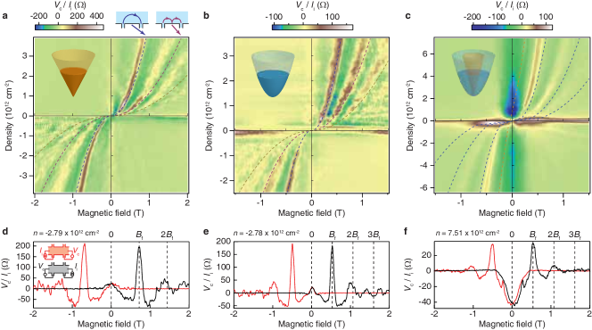
The values of can be readily calculated, since both and can be obtained from Hall measurements and the AFM image of the device, respectively. Figure 2a shows a zoom-in plot of Fig. 1e, where we have superimposed the calculated focusing fields (dashed lines) using the measured nm. A discrepancy between the calculated values and the measured peak locations is clearly present. Moreover, we find that the observed decreases as increases (Fig. 2d). The finite width of our injector and collector ( nm in MLG and BLG and nm in TLG, see below) could introduce an error in the determination of and subsequently . However, a more plausible explanation is the effect of charge accumulation near the edges owing to the finite size of our graphene devices Efetov_ChargeAccumulation . We find that charge accumulation reduces by the same order of magnitude as that required to correct for the discrepancy and, in addition, it also explains the decreasing because, for higher , the carrier’s trajectory is closer to the edge, which further reduces (see supplementary information). We also note that density fluctuations and small-angle scattering Aidala_ImagingFocusing due to impurities could also affect the carrier’s path and its focus. However, a lack of knowledge of the detailed disorder potential landscape prevents us from determining the change in the value of the focusing fields.
We have observed multiple focusing peaks in all of our devices, including BLG and TLG (see below), which indicates that a significant fraction of the electrons get specularly reflected off the graphene edge. From the peak amplitudes, we can calculate the measured specularity, the ratio between the amplitude of the second mode to that of the first mode, which offers information on the specular reflection of electrons at the graphene edges. We find that the value of specularity ranges from 0.2 to 0.5 (see supplementary information). It is worth noting that specularity measurements in semiconductor heterostructures have shown values less than 1 for focused-ion-beam etched devices which is similar to our oxygen-plasma-etched graphene devices but greater than 1 for electrostatically-defined edges Tsoi_1999 ; Houten_ElectronFocusing .

We now turn to TMF in BLG. Figures 2b and e display TMF fans for BLG at K. Evidently, the TMF spectra of MLG and BLG are very similar, even though their band structures are different (Fig. 2a-b, insets). The similarity arises from the fact that, when only the nearest intra-layer and inter-layer hopping parameters are considered, both MLG and BLG have circular Fermi surfaces, resulting in the same circular orbit and -dependence of . The dashed lines in Fig. 2b are focusing fields calculated from Eq. 1. For this device, the calculated for the first order peak are in good agreement with the measured data, but higher order modes show a discrepancy, similar to the MLG case. An additional possible source of mismatch in BLG, which does not exist in MLG, is trigonal warping McCann_BLG_g3 of the Fermi surface due to the next nearest neighbor inter-layer hopping term . This term transforms the BLG circular Fermi surface into a partly triangular surface, altering therefore the carrier’s trajectory. Hence, in principle the values of now depend on the crystallographic orientation with respect to the sample axis, and can vary by a few tens of mT (see supplementary information).
Even though TMF cannot be used to differentiate MLG from BLG, the TMF spectrum of TLG is remarkably different because of the multiband character of its band structure. Figure 2c and f show TMF spectra of TLG at K, measured at zero electric displacement field. Taking only and into account, the band structure of TLG consists of a massless MLG-like and a massive BLG-like subband at low energy (Fig. 2c, inset) Thiti_tri ; Lu_ABAbandStructure ; Guinea_ABAbandStructure ; Latil_ABAbandStructure ; Partoens_ABAbandStructure . In a magnetic field, both subbands give rise to their own TMF spectra, with the BLG-like subband having a larger due to its larger Fermi momentum (for a given ) . This allows us to identify the subband corresponding to each peak observed in the data. At high density, the peak from the MLG-like subband can be seen at mT (Fig. 2c, orange dashed line, and small sharp peaks at low field in Fig. 2f) while the peaks from the BLG-like subband are visible from mT onward (Fig. 2c, blue dashed lines). We do not observe higher order modes from the MLG-like subband, probably because they are masked by the much stronger peaks from the BLG-like subband, which contains most of the charge density.
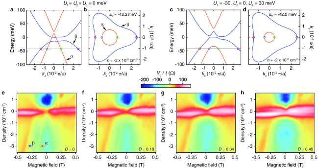
Earlier studies have shown that higher order hopping parameters in TLG significantly modify its band structure Thiti_tri ; Lu_ABAbandStructure ; Guinea_ABAbandStructure ; Latil_ABAbandStructure ; Partoens_ABAbandStructure by introducing subband overlap and trigonal warping in the BLG-like subband (Fig. 3a). We use this full parameter model for the TLG band structure to simulate the carrier trajectories and determine the focusing fields (see supplementary information). The results are shown as dashed lines in Fig 2c. Although we can reproduce the focusing field for the MLG-like subband very accurately, we obtain a mismatch in the BLG-like subband, similar to those above mentioned in MLG and BLG.
We now focus on the previously unexplored potential of TMF as a ballistic electron spectroscopy method to investigate in-situ changes in the band structure of a material. One of the remarkable properties of TLG is that its band structure can be tuned and controlled by using a transverse electric displacement field Koshino_ABA_Gate , . TMF is sensitive to the occupation of each of the TLG subbands, enabling us to use TMF as a probe of the change in the TLG band structure with . Figures 3a and b show the band structure and Fermi surface of TLG at cm-2 for the case . We denote the valence bands of the MLG-like and BLG-like subbands as and bands, respectively. The application of a finite induces a potential difference between the TLG layers, breaking the mirror symmetry and causing a hybridization between the MLG-like and BLG-like subbands. Figures 3c and d show how a finite results in a shift down of the top of the band . Consequently, for a fixed density, the Fermi momentum of the band shrinks with while that of the band barely changes due to its much higher density of states.
Figures 3e-h show the TMF spectra of TLG at various ’s. We observe a relatively strong focusing peak from the band at V/nm. However, as increases, the peak starts to shift downward and it eventually disappears at low density. The disappearance of this peak is the result of the top of the band shifting down in energy and leaving the band as a lone contributor to the carrier density (Fig. 3c-d). Therefore, within our density range, we end up observing only a single focusing peak, from the band, at high . The onset in the density of the focusing peak of the band allows us to determine the potential difference among the TLG layers as a function of applied . As a result, we can estimate the effective dielectric constant of TLG which we find to be about (see supplementary information).

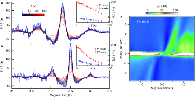
We now look at the temperature dependence of the TMF spectra in MLG and BLG. The TMF spectrum is affected by temperature, , at least in two ways: through the increase in dephasing (which smoothes the quantum interference fluctuations), and through the loss of ballistic transport due to new scattering channels activated at high . Figures 4a and b show the TMF spectra of MLG and BLG, respectively, at cm-2 from to K. We first concentrate on the fine structure observed at low (blue traces). This structure is the aforementioned quantum interference between different paths on which electrons propagate to the collector Houten_ElectronFocusing ; Beenakker_modeInterference ; Aidala_ImagingFocusing ; Rakyta_ElectronFocusingTheory . When the temperature-induced broadening of the Fermi momentum is on the order of , electrons become incoherent and the quantum interference is washed out Cheianov_VeselagoLens , resulting in smooth focusing peaks. For our devices, this length corresponds to a temperature of about K, which is in good agreement with the data.
In addition, the focusing peaks also decrease as increases. The amplitudes of the first and second modes are shown in the insets of Fig. 4a and b for MLG and BLG, respectively. We observe that the focusing amplitude in MLG depends linearly on . A potential scattering mechanism includes longitudinal acoustic phonons, which give rise to a linear temperature dependence of the scattering rate Hwang_AcousticPhonon . However, we observe a very different temperature dependence in BLG. The peak amplitude saturates at low temperature and decreases faster than in MLG at higher . A similar temperature dependence of the focusing peaks has also been observed in InGaAs/InP heterojunctions Heremans_TDependence . Further theoretical work is needed to understand the temperature dependence of the focusing peaks as well as the difference between MLG and BLG.
We end by commenting on the remarkable robustness of TMF in graphene. Fig. 4c shows the TMF fan of MLG at room temperature ( K), where the first mode is clearly visible, indicating room temperature ballistic transport well into the micron regime. This lower bound temperature for the observation of TMF in graphene is at least three times higher than the highest temperature at which TMF spectrum has been observed in semiconductor heterostructures Heremans_TDependence , the main reason probably being the lack of remote interfacial phonon scattering Guinea_TDepend_hBN from hBN. The ability to manipulate ballistic motion in graphene at room temperature, coupled with recent developments Liu_GrapheneOnhBN in large area growth of graphene on hBN, paves the way towards novel applications based on electron-optics. On a more fundamental level, TMF may serve as a probe of electron-electron interaction Novoselov_blg_interaction ; Weitz_bilayer ; CastroNeto_eeInteraction or strain-induced gauge field Guinea_strain ; Crommie_Strain ; Manoharan_graphene effects in the electronic structure of graphene.
Methods
Figure 1c shows an atomic force microscopy image from one of our devices. Our devices are fabricated by transferring graphene onto high-quality hexagonal boron nitride Dean_BN . We use oxygen plasma to etch graphene flakes into a Hall-bar geometry. Contacts are defined by electron-beam lithography and thermal evaporation of chromium and gold. The devices are then heat annealed in forming gas and subsequently current annealed in vacuum at low temperature Thiti_tri . We observe TMF peaks both before and after current annealing. The data after current annealing have higher quality than before current annealing, especially at low density, likely due to reduced charge density fluctuations. However, they exhibit similar quality at high density. All the data shown here are measured after current annealing, except Fig. 2d-e and Fig. 4a-b which was done before current annealing.
We identify the number of graphene layers by Raman spectroscopy and/or quantum Hall measurements. For TLG, the quantum Hall measurements reveal that it is Bernal-stacked Thiti_tri . In addition, we put a top gate onto the TLG device, using hBN as a thin dielectric. The combination of top gate (TG) and bottom gate (BG) allows us to control the charge density and the displacement field independently. We parameterize the displacement field by where is the capacitive coupling, is the applied gate voltage relative to the charge neutrality point, and is the vacuum permittivity.
Acknowledgements
We thank L. Levitov and A. Yacoby for discussions. We acknowledge financial support National Science Foundation Career Award No. DMR-0845287 and the Office of Naval Research GATE MURI. This work made use of the MRSEC Shared Experimental Facilities supported by the National Science Foundation under award No. DMR-0819762 and of Harvard s Center for Nanoscale Systems (CNS), supported by the National Science Foundation under grant No. ECS-0335765.
Author contributions
T. Taychatanapat fabricated the samples and performed the experiments. K.W. and T. Taniguchi synthesized the hBN samples. T. Taychatanapat and P.J-H. carried out the data analysis and co-wrote the paper.
Additional information
Correspondence and requests for materials should be addressed to P.J-H. (email: pjarillo@mit.edu)
References
- (1) Bloch, F. Über die Quantenmechanik der Elektronen in Kristallgittern. Z. Phys. 52, 555–600 (1929).
- (2) Tsoi, V. S. Focusing of electrons in a metal by a transverse magnetic field. JETP Lett. 19, 70–71 (1974).
- (3) Tsoi, V. S., Bass, J. & Wyder, P. Studying conduction-electron/interface interactions using transverse electron focusing. Rev. Mod. Phys. 71, 1641–1693 (1999).
- (4) van Houten, H. et al. Coherent electron focusing with quantum point contacts in a two-dimensional electron gas. Phys. Rev. B 39, 8556–8575 (1989).
- (5) Rokhinson, L. P., Larkina, V., Lyanda-Geller, Y. B., Pfeiffer, L. N. & West, K. W. Spin separation in cyclotron motion. Phys. Rev. Lett. 93, 146601 (2004).
- (6) Goldman, V. J., Su, B. & Jain, J. K. Detection of composite fermions by magnetic focusing. Phys. Rev. Lett. 72, 2065–2068 (1994).
- (7) Smet, J. H. et al. Magnetic focusing of composite fermions through arrays of cavities. Phys. Rev. Lett. 77, 2272–2275 (1996).
- (8) Dean, C. R. et al. Boron nitride substrates for high-quality graphene electronics. Nature Nanotech. 5, 722–726 (2010).
- (9) Taychatanapat, T., Watanabe, K., Taniguchi, T. & Jarillo-Herrero, P. Quantum Hall effect and Landau-level crossing of Dirac fermions in trilayer graphene. Nature Phys. 7, 621–625 (2011).
- (10) Mayorov, A. S. et al. Micrometer-scale ballistic transport in encapsulated graphene at room temperature. Nano Lett. 11, 2396–2399 (2011).
- (11) Du, X., Skachko, I., Barker, A. & Andrei, E. Y. Approaching ballistic transport in suspended graphene. Nature Nanotech. 3, 491–495 (2008).
- (12) Bolotin, K. I., Sikes, K. J., Hone, J., Stormer, H. L. & Kim, P. Temperature-dependent transport in suspended graphene. Phys. Rev. Lett. 101, 096802 (2008).
- (13) Beenakker, C. W. J., van Houten, H. & van Wees, B. J. Mode interference effect in coherent electron focusing. Europhys. Lett. 4, 359–364 (1988).
- (14) Aidala, K. E. et al. Imaging magnetic focusing of coherent electron waves. Nature Phys. 3, 464–468 (2007).
- (15) Rakyta, P., Kormányos, A., Cserti, J. & Koskinen, P. Exploring the graphene edges with coherent electron focusing. Phys. Rev. B 81, 115411 (2010).
- (16) Silvestrov, P. G. & Efetov, K. B. Charge accumulation at the boundaries of a graphene strip induced by a gate voltage: Electrostatic approach. Phys. Rev. B 77, 155436 (2008).
- (17) McCann, E. & Fal’ko, V. I. Landau-level degeneracy and quantum Hall effect in a graphite bilayer. Phys. Rev. Lett. 96, 086805 (2006).
- (18) Lu, C. L., Chang, C. P., Huang, Y. C., Chen, R. B. & Lin, M. L. Influence of an electric field on the optical properties of few-layer graphene with AB stacking. Phys. Rev. B 73, 144427 (2006).
- (19) Guinea, F., Neto, A. H. C. & Peres, N. M. R. Electronic states and Landau levels in graphene stacks. Phys. Rev. B 73, 245426 (2006).
- (20) Latil, S. & Henrard, L. Charge carriers in few-layer graphene films. Phys. Rev. Lett. 97, 036803 (2006).
- (21) Partoens, B. & Peeters, F. M. From graphene to graphite: Electronic structure around the K point. Phys. Rev. B 74, 075404 (2006).
- (22) Koshino, M. & McCann, E. Gate-induced interlayer asymmetry in ABA-stacked trilayer graphene. Phys. Rev. B 79, 125443 (2009).
- (23) Cheianov, V. V., Falḱo, V. & Altshuler, B. L. The focusing of electron flow and a veselago lens in graphene p-n junctions. Science 315, 1252–1255 (2007).
- (24) Hwang, E. H. & Das Sarma, S. Acoustic phonon scattering limited carrier mobility in two-dimensional extrinsic graphene. Phys. Rev. B 77, 115449 (2008).
- (25) Heremans, J., Fuller, B. K., Thrush, C. M. & Partin, D. L. Temperature dependence of electron focusing in In1-xGaxAs/InP heterojunctions. Phys. Rev. B 52, 5767–5772 (1995).
- (26) Schiefele, J., Sols, F. & Guinea, F. Temperature dependence of the conductivity of graphene on boron nitride. Phys. Rev. B 85, 195420 (2012).
- (27) Liu, Z. et al. Direct growth of graphene/hexagonal boron nitride stacked layers. Nano Lett. 11, 2032–2037 (2011).
- (28) Mayorov, A. S. et al. Interaction-drive spectrum reconstruction in bilayer graphene. Science 333, 860–863 (2011).
- (29) Weitz, R. T., Allen, M. T., Feldman, B. E., Martin, J. & Yacoby, A. Broken-symmetry states in doubly gated suspended bilayer graphene. Science 330, 812–816 (2010).
- (30) Kotov, V. N., Uchoa, B., Pereira, V. M., Guinea, F. & Castro Neto, A. H. Electron-electron interactions in graphene: Current status and perspectives. Rev. Mod. Phys. 84, 1067–1125 (2012).
- (31) Guinea, F., Katsnelson, M. I. & Geim, A. K. Energy gaps and a zero-field quantum Hall effect in graphene by strain engineering. Nature Phys. 6, 30–33 (2010).
- (32) Levy, N. et al. Strain-induced pseudo-magnetic fields greater than 300 tesla in graphene nanobubbles. Science 329, 544–547 (2010).
- (33) Gomes, K. K., Mar, W., Ko, W., Guinea, F. & Manoharan, H. C. Designer Dirac fermions and topological phases in molecular graphene. Nature 483, 306–310 (2012).