, ,
Dynamical transport properties of NbSe3 with simultaneous sliding of both charge density waves
Abstract
Measurements of the nonlinear conductivity in NbSe3 when the high-T and the low-T charge-density waves (CDWs) are simultaneously sliding have been performed. It is shown that the threshold electric field, , for depinning the high-T CDW increases 4 - 5 times at the temperature at which the low-T CDW is formed, indicating the strong pinning effect resulting from the interaction between both CDWs. Under application of a radio-frequency (rf) field, Shapiro steps are never observed simultaneously for both CDWs. At the electric field less one than for high-T CDW sliding only Shapiro steps for low-T CDW were observed, and at higher field only Shapiro steps for high-T CDW exist.
pacs:
71.45.Lr, 72.15.Nj, 72.70.+m,I INTRODUCTION
NbSe3 is an emblematic quasi-one-dimensional metal with three pairs of metallic chains (types I, II, and III) parallel to the monoclinic direction ECRYS11 . NbSe3 undergoes two successive Peierls transitions: at K with a charge density wave (CDW) essentially on type I chains and at K with a CDW essentially on type II chains Gruner . The wave vectors of both CDWs are respectively: and . The Peierls transitions in this material are not complete and ungapped carriers remain in small pockets at the Fermi level most probably associated with type III chainsShima ; SinchenkoJPCM09 . As a result, NbSe3 keeps metallic properties down to the lowest temperatures. Application of an electric field above a threshold value for high-T CDW and for low-T CDW induces a collective electron transport due to the coherent incommensurate CDW motion Gorkov89 ; Monceau12 .
One general question immediately arises when several order parameters coexist in the same material, such as the two CDWs in NbSe3: are they totally independent or are they interacting one with the other? If yes, what is the result and the mechanism of this interaction? Several attempts were already undertaken for answering this question. X-ray scattering measurements on pinned CDWs showed no sign of a lock-in transition Fleming83 which may be envisioned such as:
| (1) |
From interlayer tunneling techniqueOrlov06 it was found that resulting from the low-T CDW formation the CDW gap of the high-T CDW exhibits a 10% decrease below .
As far as the dynamical properties associated with both high-T and low-T CDWs at temperatures are concerned, contradictory data were reported. In Refs.Gill80, ; Richard80, it was indicated that the depinning field, , of the high-T CDW may saturate below while according to Ref.Fleming80, continuously grows without any peculiar singularity at .
From high-resolution x-ray scattering in the presence of an applied current below , simultaneous and oppositely directed shifts of the relevant CDW-superlattice components along chains were observed above a threshold current which was identified as the depinning threshold for the more strongly pinned high-T CDW.Ayari04 This dynamical decoupling was explained through a sliding-induced charge transfer between the two electronic reservoirs corresponding to the CDW wave vectors and . Using the same technique but in a different context related to switching effects in NbSe3, a dynamical coupling was reported from analysis of the transverse structure of both CDWs.Noh01 Note that in all these works was not directly determined from non-linear current-voltage characteristics (IVs) below 60 K but estimated as being the field at which broadband noise (BBN) increased; there is a large uncertainty in this determination (see for instance Fig. 2 in Ref.Ayari04, ).
Thus, at the present time, there are no complete and reliable measurements describing dynamical properties of NbSe3 in the temperature range corresponding to the coexistence of both CDWs. In the following we report, for the first time, from current-voltage characteristics (IVs), the observation of the simultaneous sliding behavior for both CDWs. The sliding state of each CDWs is confirmed by the observation of Shapiro steps when an radio-frequency electric field is applied together with the dc electric field. The present work extends the previous reportSinchenko12a where Shapiro steps were observed separately for each CDW.
II Experimental technique
The main problem for the determination of the threshold behavior of the high-T CDW at temperature below from IV characteristics is Joule heating. On the one hand, to reduce heating one needs to use samples with high resistance and correspondingly with a small cross-section. On the other hand, decrease of the crystal cross-section leads to an exponential grow of because of finite size effects.McCarten92 We have found that the compromise between the best thermal conditions and the magnitude of the threshold field takes place by selecting crystals with a thickness (0.4 - 0.6) m and for resistance at room temperature in the range 0.5 - 2.0 k/mm. So, we performed our experiments on three selected high quality NbSe3 single crystals with a thickness indicated above and a width (2 - 8)m. The residual resistance ratio of the selected crystals was . The crystals were cleaned in oxygen plasma and glued on sapphire substrates by collodion. The measurements of IV characteristics and their derivatives have been done in conventional 4-probe configuration. Contacts were prepared from In by cold soldering. The distance between the potential probes was 1 mm for all the samples. For studying nonstationary effects a rf current was superposed on the dc current using the current contacts connected to the rf generator via two capacitors.
III Experimental results
In Fig.1, we have drawn the differential current-voltage characteristics (IVs) in the temperature range 135 - 46 K for sample No.2. The qualitatively same characteristics were observed for two other samples. The threshold behavior corresponding to the sliding state of the high-T CDW is clearly seen from 135 K down to 90 K: the behavior is Ohmic for voltage less than a threshold voltage , and for voltages in excess of this value the differential resistance, , decreases sharply. As usual decreases from down to 120 K and monotonically increases at lower temperatures.
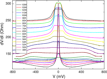
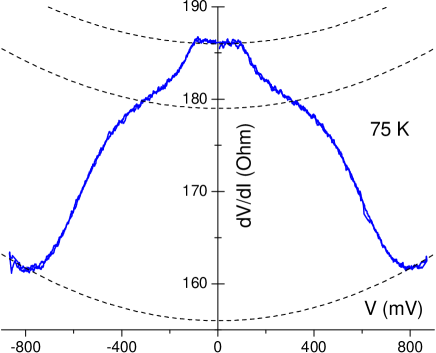
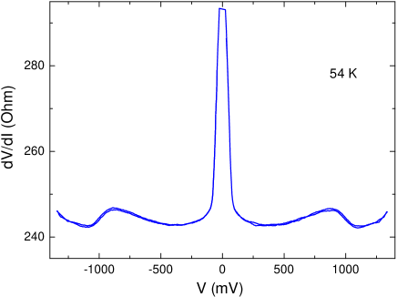
Below 90 K a new decrease of appears at a certain voltage that is nearly times larger than and becomes more and more pronounced in lowering temperature. As an example of such behavior the dependence at K is shown in Fig.2. When is reduced, the amplitude of the change in at from static to sliding decreases while that at increases. At the first threshold at is completely indiscernible, and only the second threshold at remains. Below we observe the threshold behavior for the low-T CDW at the voltage that is near to times less than . Fig.3 clearly demonstrates the singularities in the IV curve for sample No.3 corresponding to the transition into the sliding state of both CDWs at K.
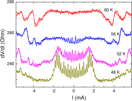
To prove that non-linear effects observed in dc IV curves are really associated with CDWs sliding, we have superposed a rf current on the dc current. It is well known that the joint application of dc and rf driving fields leads to appearance of harmonic and sub-harmonic Shapiro steps in the dc IV characteristics indicating sliding state of CDWECRYS11 ; Gorkov89 ; Monceau12 . Differential IV characteristics for sample No.3 in the temperature range 48 - 100 K under application of a rf field with a frequency 101 MHz are shown in Fig.4. The Shapiro steps appear when and reflects the synchronisation between the internal CDW sliding state and the external frequency. As can be seen, at K the Shapiro steps corresponding to the high-T CDW are observed at . Note that in the temperature range 60 - 90 K the Shapiro steps peculiarities are sufficiently weak compared with those at other temperatures.
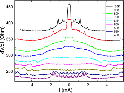
Below we observe pronounced Shapiro steps for both CDWs as illustrated in Fig.5 where IV curves at 60, 56, 52 and 48 K are displayed. Typically the rf amplitude was larger compared with and less than . Consequently the dc threshold at is totally suppressed Zettl84 while the threshold at is still observable. It is worth to note that Shapiro steps corresponding to the low-T CDW disappear at voltages and only Shapiro steps associated with the high-T CDW are observable at these voltages.
IV Discussion
First of all let ascertain that the drop of observed at really corresponds to the sliding of the high-T CDW. It is well known that the fundamental frequency of the narrow-band generation is directly proportional to the CDW currentECRYS11 ; Gorkov89 ; Monceau12 :
| (2) |
where is the number of carriers condensed into the CDW at temperature , and is a constant. As far as Shapiro steps are concerned it is necessary to change in equation (2) to which corresponds to the difference of CDW current between two neighboring harmonic Shapiro steps. can be easy calculated using dc IV-characteristics. We have calculated the relation of for the high-T CDW at temperatures below and above and for the low-T CDW for all measured samples. Estimations for sample No.2 for the high-T CDW at temperatures K and 54K and for the low-T CDW at K with the frequency of the rf field at MHz are respectively 1.10; 1.17 and 1.28 A/MHz. In accordance with Ref.Richard82, , we can derive from our experiments that the number of condensed carriers into the CDW state is practically equal for the low- and high-T CDW. Thus, we associate the observed sharp drop in dependencies at with the transition to the sliding state of the high-T CDW.
Using our dc curves we have also estimated the respective CDW velocities when both CDWs are in a sliding state. Thus for sample No.3 at K at the given total transport current mA, we have evaluated mA and mA. Taking for cm (Ref.Richard82, ) and 2.4 m2 for the cross-section area the CDW velocities are respectively cm/s for the low-T CDW and cm/s for the high-T CDW. So, in the state when both CDWs are in the sliding state the velocity of high-T CDW near one order of magnitude higher than that of the low-T CDW.
In addition we can conclude that at K the sliding of the high-T CDW is characterized by two threshold fields: and . The change in conductivity associated with these two thresholds (indicated by the dashed lines in fig.2 ) is different: when the temperature decreases, the change of conductivity below decreases while that below increases. At K there are no more sign of the threshold.
Fig.6 shows the temperature dependencies of threshold fields for high- and low-T CDWs for sample No.2 in logarithmic scale. The same characteristics were observed for other samples. The demonstrates a conventional behavior. The (T) decreases with the temperature decrease from 90 down to 60 K and remains nearly constant or demonstrates some tendency to increase at K. The temperature range of the observation of the coexistence between the two thresholds and is indicated by the dotted lines. Note, that this temperature region corresponds well to that where low-T CDW fluctuations were observedBrun10 . The temperature dependence of low-T threshold field is in agreement with previous reported dataFleming80 .
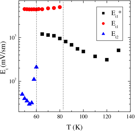
We can suggest the following physical picture. Above 60 K the sample may be considered as consisting, in addition to the ordered high-T CDW, of domains of low-T CDW fluctuations. Then the assumption is that these fluctuations strongly pin the high-T CDW. Most probably, the mechanism of this pinning may be a dynamical commensurability pinning between the ordered high-T CDW and fluctuations of low-T CDW.
As a result, in the temperature range between 60 and90 K the sliding of the high-T CDW exhibits two threshold fields reflecting the mixing of two types of domains. With the temperature growing the size of fluctuation regions decreases and becomes negligibly small at K where only the phase with has been observed. Inversely, at K only the phase with exists. At temperatures K both phases are in the near equal proportion; as a result the Shapiro steps are essentially smeared at this temperature range.
Another interesting observation of the present work is the unusual structure of Shapiro steps when both CDWs exist simultaneously. As it was mentioned above, in such a condition Shapiro steps corresponding to the low-T CDW disappear at voltages and only Shapiro steps associated with the high-T CDW are observable at these voltages (Fig.5). Formally it may mean that the motion of the high-T CDW suppresses the narrow-band-noise generation from the low-T CDW. The complete explanation of this effect is missing now.
Recently, a new view on the origin of the narrow band noise generation in CDW compounds was suggestedSinchenko12a , namely that Shapiro steps in CDW compounds are the result of electronic transport transversely to CDW chains. Such assumption is based on theory proposed in Refs.ArtemenkoVolkov84, ; Artemenko97, where it was predicted that the transverse current has a term proportional to the cosine of the difference of phases between the CDW chains. In the case when the CDW slides along one chain but is pinned along neighbouring chains, or if the CDW moves with different velocities in different chains, or if the CDW is pinned but phase slippage takes place, then the CDW phase varies with time and alternating tunneling current is generated transversely to the chain direction with a frequency depending on the longitudinal electric field. When an external alternating signal acts on the sample, a resonance can be observed at a fixed if the frequencies of the external and characteristic oscillations coincide. As a result, current Shapiro steps should appear in transverse IVc that was really observed in experimentSinchenko12a . In real samples the appearance of an electric potential normal to the transport current exists always and has been attributed to defects and fluctuations of the critical CDW parameters such as threshold electric field or Peierls transition temperature.Sinch11 . It is then natural to assume that synchronisation of the generated frequencies in NbSe3 will be strongly dependent on the state of all types of chains. Thus, sliding of high-T CDW strongly modifies the transverse current distribution in the sample, and as a result may destroy the synchronisation frequencies resulting for low-T CDW sliding. However, to clarify the physical mechanism of this effect new theoretical and experimental investigations need to be performed.
In conclusion, we clearly observed for the first time the nonlinear conductivity in current-voltage characteristics of NbSe3, corresponding to simultaneous sliding of both, the high-T and the low-T, charge-density waves. We show that the interaction between CDWs leads to strong pinning of the high-T CDW and resulting to times increase of threshold electric field. In the temperature range up to 30 K above the second Peierls transition the sliding of the high-T CDW exhibits two thresholds, most probably because of the local fluctuations of the low-T CDW. The superposition of an rf current on the dc current leads to appearance of Shapiro steps on dc IV curves for low-T CDW at and for high-T CDW at . Both types of Shapiro steps have never been observed simultaneously.
Acknowledgements.
The authors are thankful S.V. Zaitsev-Zotov and S.G. Zybtsev for helpful discussions of the experimental results. The work has been supported by Russian State Fund for the Basic Research (No. 11-02-01379- ), and partially performed in the frame of the CNRS-RAS Associated International Laboratory between CRTBT and IRE ”Physical properties of coherent electronic states in coherent matter”. The support of ANR-07-BLAN-0136 is also acknowledged.References
- (1) Electronic Crystals 2011 edited by S. Brazovskii, P. Monceau and N. Kirova, (Physica B, vol 407, Issues 11, 2012).
- (2) G. Grüner, Density Waves in Solids (Addison – Wesley, Reading, Massachusetts, 1994)
- (3) Shima N and Kamimura H 1985 Theoretical Aspects of Band Structure and Electronic Properties of Pseudo- One-Dimensional Solids (Dordrecht: Reidel)
- (4) A.A. Sinchenko, R.V. Chernikov, A.A. Ivanov, P. Monceau, Th. Crozes and S.A. Brazovskii, J. Phys.: Condens. Matter 21, (2009) 435601.
- (5) L. Gor’kov and G. Grüner Charge Density Waves in Solids (Amsterdam: Elsevier Science, 1989)
- (6) P. Monceau, Advances in Physics 61, (2012) 325 581
- (7) R.M. Fleming, C.H. Chen and D.E. Moncton, J. Physique (France) 44, (1983) C3-1651.
- (8) A.P. Orlov, Yu.I. Latyshev, A.M. Smolovich and P. Monceau, JETP Lett. 84, 89, 2006.
- (9) J.C. Gill, J. Phys. F 10, L81 (1980).
- (10) J. Richard and P. Monceau, Solid State Commun. 33, 635 (1980).
- (11) R.M. Fleming, Phys. Rev. B 22, 5606 (1980).
- (12) A. Ayari, R. Danneau, H. Requardt, Ortega, J. E. Lorenzo, P. Monceau, R. Currat, S. Brazovskii, and G. Gru bel, Phys.Rev. Lett. 93, (2004) 106404.
- (13) Y. Li, D. Y. Noh, J. H. Price, K. L. Ringland, J. D. Brock, S. G. Lemay, K. Cicak, R. E. Thorne, Mark Sutton, Phys. Rev. B 63, 041103(R) (2001).
- (14) A.A. Sinchenko, P. Monceau, and T. Crozes, Phys. Rev. Lett. 108, 046402 (2012).
- (15) J. McCarten, D.A. DiCarlo, M.P. Maher, T.L. Adelman, and R.E. Thorne, Phys. Rev. B 46, 4456 (1992).
- (16) A. Zettl and G. Grüner, Phys. Rev. B 29, 755 (1984).
- (17) J. Richard, P. Monceau and M. Renard, Phys. Rev. B 25, 948 (1992).
- (18) Ch. Brun, Zhao-Zhong Wang, P. Monceau, and S. Brazovskii, Phys. Rev. Lett. 104, 256403 (2010).
- (19) S.N. Artemenko and A.F. Volkov, Sov. Phys. JETP 60, (1984), 395; JETP Lett., 83, (1983), 368.
- (20) S.N. Artemenko, JETP 84, (1997), 823.
- (21) A.A. Sinchenko, P. Monceau and T. Crozes, JETP Lett. 93, (2011), 56.