Quantum Hall Effect in Hydrogenated Graphene
Abstract
The quantum Hall effect is observed in a two-dimensional electron gas formed in millimeter-scale hydrogenated graphene, with a mobility less than 10 and corresponding Ioffe-Regel disorder parameter . In zero magnetic field and low temperatures, the hydrogenated graphene is insulating with a two-point resistance of order of . Application of a strong magnetic field generates a negative colossal magnetoresistance, with the two-point resistance saturating within 0.5% of at 45T. Our observations are consistent with the opening of an impurity-induced gap in the density of states of graphene. The interplay between electron localization by defect scattering and magnetic confinement in two-dimensional atomic crystals is discussed.
Two-dimensional atomic crystals have attracted much attention as surfaces with unique low-dimensional electron transport behaviour, most notably the zero-gap semiconductor graphene Novoselov04 . The relativistic Dirac dispersion of electrons in graphene leads to an anomalous four-fold degenerate quantum Hall (QH) sequence Novoselov05 ; Zhang05 ; Zhang06 ; Young12 . Common to these studies is low disorder, with a mean free path large compared to electron Fermi wavelength , with the cleanest graphene samples exhibiting the fractional quantum Hall (FQH) effect Du09 ; Dean11 . We report here our discovery of a quantum Hall effect in graphene at the opposite extreme, whereby hydrogenation was used to induce a short mean-free path beyond the Ioffe-Regel limit for the onset of strongly insulating behaviour. Our work illustrates the importance of the interplay between electron localization by point defect scattering and magnetic confinement in two-dimensional atomic crystals.
We present experimental results on electronic transport in graphene where neutral point defects are introduced by hydrogenation. Previous electron transport studies of hydrogenated graphene were interpreted as evidence for graphaneElias09 , a two-dimensional polymer of carbon and hydrogen. More recently, angle resolved photo-emission spectroscopy (ARPES) Grueneis10 and scanning tunneling microscopy (STM) Grueneis12 measurements have demonstrated the opening of a gap in the density of states of hydrogenated graphene. The object of our work is to probe the magnetotransport properties of hydrogenated graphene. We focus on large area (millimeter-scale) graphene that was exposed to an atomic hydrogen beam resulting in insulating behaviour ( at zero magnetic field) and a low-temperature resistance far above the Ioffe-Regel limit for the onset of insulating behaviour. Application of a magnetic field induces a transition to a well formed quantum Hall state with a two point resistance accurate to within . The insulator-quantum Hall transition coincides with the magnetic length () approaching, and becoming less than the mean defect spacing inferred from Raman spectroscopy ().
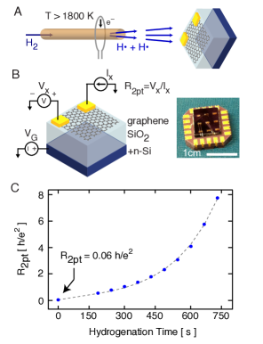
Disordered graphene samples were prepared from pristine, large-area, monolayer graphene samples grown by chemical vapour deposition (CVD) on Cu foils Ruoff09 , with growth details reported elsewhere guermoune11 . Graphene monolayers were transferred to oxidized silicon wafers and electrically contacted for electron transport experiments. Disorder was controllably introduced into the graphene by exposure to a beam of atomic hydrogen produced by thermally cracking molecular hydrogen with a white-hot tungsten capillary Bischler93 . The room temperature two-point resistance of graphene samples was monitored versus atomic hydrogen exposure in situ in an ultra-high vacuum chamber, Fig.1. The room temperature resistance of graphene devices was observed to increase with exposure to atomic hydrogen, as has been observed in graphene exposed to hydrogen plasma Elias09 . Atomic hydrogen exposure produces an exponential growth in resistance, and a corresponding exponential shortening of carrier mean-free path . The Ioffe-Regel disorder parameter , where accounts for spin and valley degeneracy, is consequently significantly increased beyond the limit for the onset of strongly insulating behaviour.
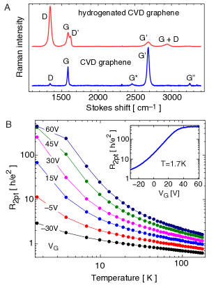
The disorder introduced by hydrogenation was observed by Raman spectroscopy, Fig. 2A. The Raman Stokes peaks G and G’ associated with pristine carbon indicate clean, monolayer CVD graphene prior to hydrogenation (blue spectrum). The emergence of strong disorder-induced peaks D and D’ upon hydrogenation (red spectrum) confirms the introduction of point defects that break the translational invariance of the crystal Jorio11 . The nature of the point defects introduced by hydrogenation is most likely hydrogen-carbon bonds Elias09 . By direct comparison of the ratio of D peak intensity to G peak intensity, , with that observed in graphene disordered by controlled ion bombardment Lucchese10 , we estimate the mean hydrogen-hydrogen spacing to be in the range for a 360s hydrogen exposure, corresponding to a hydrogen to carbon ratio.
Electronic transport measurements were performed on the hydrogenated graphene with large ohmic contacts at the opposing corners of a 2.5 mm square using a standard low-frequency technique. The hydrogenated graphene shows unambiguous insulating behaviour, , over the entire range of accessible temperatures (from 175K to 1.7K) and gate induced carrier density, Fig.2B. Gate voltage modulation of the resistance shows hole transport with a field effect mobility , where the gate capacitance . A regime of zero field effect mobility is also observed, see inset of Fig. 2B, where the Ioffe-Regel parameter is . In contrast, the Ioffe-Regel parameter in Si Klitzing80 and GaAs/AlGaAs Tsui82 where QH and FQH was first observed is . The exponential increase in resistance as appears consistent with a variable-range hopping behaviour , however we do not find good agreement to either a Mott or Efros-Shklovskii exponent over the temperature range . Rather, a pronounced saturation in resistance is observed at the lowest hole density and lowest temperatures, corresponding to the emergence of a zero field effect mobility regime of transport.
The 2-point resistance was measured at versus carrier density and in strong magnetic fields, Fig.3A. At high hole densities, a colossal negative magnetoresistance is observed from through to . A similar magnetoresistance was observed in weakly fluorinated graphene hong11 . Conversely, in the regime of zero field effect mobility, the resistance is very weakly dependent on magnetic field below a critical field that is itself dependent upon gate voltage. Remarkably, at a gate voltage , a sharp transition is observed from an insulating, zero field effect mobility state, to a resistance saturating at a value , which is within of . In a quantum Hall state, the longitudinal four point resistance so that the two point resistance approaches the transverse resistance . The behaviour of is fully consistent with a Hall component admitting the quantized value . From the known anomalous QH series of graphene Novoselov05 ; Zhang05 , the hole doping of the sample, and an assumption of preserved spin and valley degeneracies, this QH state corresponds to the Landau level index and a filling factor. Notably, no Shubnikov-de Haas oscillations in resistance are observed as this QH state is reached at high magnetic field.
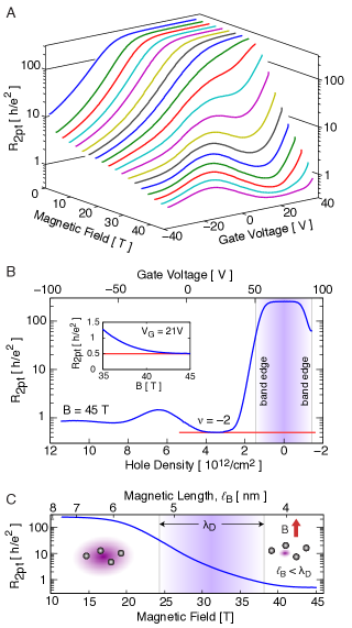
The resistance versus gate voltage at constant , Fig.3B, reveals the charge neutrality point at between electron and hole conduction. The hole density at required by the magnetic flux density is , while the plateau is observed with holes induced from neutrality. The mobile hole valence band edge is thus located at gate voltage , providing a signature in electron transport of the formation of a disorder induced gap. Assuming electron-hole symmetry about charge neutrality, we estimate a localized mid-gap state density of . Gap opening and the presence of mid-gap states have been observed in hydrogenated graphene by ARPES Grueneis10 and STM Grueneis12 , with a gap of observed for a similar hydrogen to carbon ratio. Neither the or plateaus are clearly observed, however the weak resistance minimum at hints to an emerging QH state. Disorder induced broadening of Landau levels may be responsible for the absence of other plateaus and the absence of Shubnikov-de Haas oscillations.
From the perspective of two-dimensional transport in a disordered medium, the emergence of a quantum Hall state at from a zero-field insulating state induced by neutral point defects can be understood by comparison of length scales, Fig.3C. The magnetic length quantifies the magnetic confinement of charge carriers in 2D, independent of material parameters. The insulator-QH transition is here observed with magnetic length spanning , consistent with a crossover from weak to tight magnetic confinement with respect to the point defect spacing inferred from Raman spectroscopy. The perspective of an insulator-QH transition arising from magnetic confinement of charge carriers below the mean defect spacing is complementary to the picture of extended states floating in energy that has been previously used to explain insulator-QH transitions Sankar .
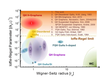
The emergence of a quantum Hall state from a zero field effect mobility insulating state raises the question of how much disorder can be introduced into a 2D electron gas (2DEG) and still form a quantum Hall state. A diagram summarizing 2DEG systems where the quantum Hall effect (QHE) has been observed is plotted in Fig.4 versus the dimensionless Ioffe-Regel disorder parameter , with the transport mean free path, and the dimensionless Wigner-Seitz radius quantifying interaction strength. The preponderance of 2DEGs where the QHE has been observed are low-disorder samples satisfying the Ioffe-Regel criterion (in zero magnetic field) . However, a previous study in disordered GaAs/AlGaAs heterostructures biased to subthreshold conditions exhibited strong disorder at low carrier density and a transition from localization to a QH stateJiang93 . Our observations with hydrogenated graphene pushes the limit of disorder to where the QHE can still be attained in a strong magnetic field, suggesting that the QHE might be robust to arbitrarily large disorder.
The insulator-QH transition in hydrogenated graphene opens a new regime in energy scales previously unavailable to experiments. The Landau level energy gap about the Landau level is Zhang05 , giving at . Previous reports of ARPES of graphene hydrogenated to a hydrogen-carbon ratio gives an estimated zero-field gap of Grueneis10 . In comparison, the bandgap of GaAs, the choice material for high mobility 2DEGs, is which is larger than the cyclotron energy separating Landau levels at . We propose that the energy scales experimentally accessible in hydrogenated graphene enable the study of the competition between disorder and magnetic confinement, leading to new understanding of the role of disorder in the QHE.
Acknowledgments
We acknowledge useful discussions with A. Grueneis (IFW Dresden), and the outstanding technical assistance of D. Berry, M. Nannini, R. Talbot, J. Smeros, R. Gagnon (McGill) as well as T.P. Murphy, J. Pucci and G. Jones (NHMFL). This work was funded by the Natural Sciences and Engineering Research Council of Canada (NSERC), the Canadian Institute for Advanced Research (CIFAR), the Fonds de Recherche du Québec - Nature et Technologies (FRQNT), and the Canada Research Chair program (CRC). A portion of this work was performed at the National High Magnetic Field Laboratory which is supported by NSF Cooperative Agreement No. DMR-0084173, the State of Florida, and the DOE.
References
- (1)
- (2) K.S. Novoselov et al., Science 306, 696 (2004).
- (3) K.S. Novoselov et al., Nature 438, 197 (2005).
- (4) Y. Zhang, Y.-W. Tan, H.L. Störmer, and P. Kim, Nature 438, 201 (2005).
- (5) Y. Zhang et al., Phys. Rev. Lett. 96, 136806 (2005).
- (6) A.F. Young et al., Nat. Physics 8, 550 (2012).
- (7) X. Du, I. Skachko, F. Duerr, A. Luican, and E.Y. Andrei, Nature 462, 192 (2009).
- (8) C.R. Dean et al., Nat. Physics 7, 693 (2011).
- (9) D.C. Elias et al., Science 323, 610 (2009).
- (10) D. Haberer et al., Nano Lett. 10, 3360 (2010).
- (11) D. Haberer et al., ACS Nano, in print (2012).
- (12) X.S. Li et al. Science 324, 1312 (2009).
- (13) A. Guermoune et al., Carbon 49, 4204 (2011).
- (14) U. Bischler and E. Bertel, J. Vac. Sci. Tech. A 11, 458 (1993).
- (15) A. Jorio et al., Raman Spectroscopy in Graphene Related Systems, Wiley-VCH, Singapore, 2011.
- (16) M.M. Lucchese et al., Carbon 48, 1592 (2010).
- (17) K. von Klitzing, G. Dorda, and M. Pepper, Phys. Rev. Lett. 45, 494 (1980).
- (18) D.C. Tsui, H.L. Störmer, and A.C. Gossard, Phys. Rev. Lett. 48, 1559 (1982).
- (19) X. Hong et al., Phys. Rev. B 83, 085410 (2011).
- (20) S. Das Sarma and A. Pinczuk, Eds, Perspectives in Quantum Hall Effects: Novel Quantum Liquids in Low-Dimensional Semiconductor Structures, p. 23, Wiley-VCH, Singapore, 1996.
- (21) H.-W. Jiang et al., Phys. Rev. Lett. 71, 1439 (1993).
- (22)
Supplementary Information
J. Guillemette1,2, S.S. Sabri2, B. Wu1, K. Bennaceur1, P.E. Gaskell2, M. Savard1, P.L. Lévesque3, F. Mahvash2,4, A. Guermoune2,4, M. Siaj4, R. Martel3, T. Szkopek2†, and G. Gervais1†⋆
I SUPPLEMENTARY INFORMATION
II Device fabrication
Graphene monolayers were grown by chemical vapour deposition (CVD) on electropolished thick copper foils with a methane precursor. Complete CVD growth procedures are described in detail in previous work guermoune11 , including the dependence of material quality on growth parameters. Graphene monolayers were transferred to oxidized silicon substrates using a thin poly-methylmethacrylate handle layer, sacrificial etching of the Cu foil in a 0.1M (NH4)2S2O8 room temperature solution. The substrates were thick As doped Si with room temperature resistivity. A chlorinated, dry thermal oxide of 300 nm thickness was used as the back-gate dielectric. After graphene transfer, a shadow mask was used to deposit Ti/Au (2 nm/50 nm) Ohmic contacts 3 mm apart. A scribe was used to manually isolate individual graphene squares on the substrate surface.
Hydrogenation was performed in a UHV chamber with a base pressure in the low Torr range. A custom-built capillary atomic hydrogen source Bischler93 was used. A tungsten capillary was heated to by electron bombardment, with power at acceleration voltage. A beam of thermally cracked hydrogen was produced upon introduction of molecular hydrogen to the capillary through a leak valve at an approximate chamber pressure of Torr. The graphene samples were mounted away from the hydrogen source, with a shutter used to precisely control device exposure. All devices were subjected to a 1 hour thermal anneal at 400 K prior to hydrogen exposure to degas the sample surface. Between hydrogen doses, in situ measurement of electrical resistance was performed, allowing the effect of hydrogenation on electrical resistance to be monitored.
III Raman spectroscopy
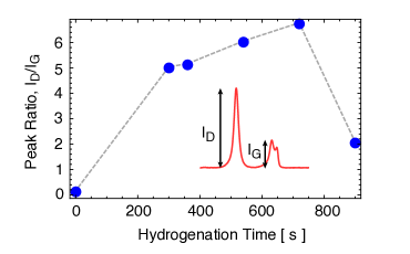
Raman spectroscopy was performed on CVD graphene and hydrogenated CVD graphene with a pump laser of 20 mW incident power and a pump laser of 20 mW incident power, both through a 40 objective. All measurements were performed with graphene on oxidized silicon, with 4 distinct spatial regions probed. With the pump, the Raman peaks observed in CVD graphene (Fig. 1A) were D (1347 cm-1), G (1588 cm-1), G* (2462 cm-1), G’ (2685 cm-1) and G” (3255 cm-1). The D peak was more intense relative to G in the hydrogenated graphene sample used for high-field transport measurements, and new Raman peaks associated with increased disorder Jorio11 emerged: G+D (2942 cm-1) and D’ (1628 cm-1). The evolution of the ratio of D peak intensity () to G peak intensity() versus hydrogenation time of six CVD graphene samples is plotted in Fig.5. A non-monotonic behaviour in versus hydrogen dose is found, similar to the evolution of versus Ar+-ion bombarded graphene Lucchese10 . Under the assumption of similar point-defect induced Raman spectra by hydrogenation as by Ar+-ion bombardment, the observed saturation in corresponds to a mean defect spacing .
The hydrogenated sample (#HG30) used for high-field (45 T) electron transport measurements reported here was analyzed with greater precision by Raman spectroscopy within 4 days of electron transport measurement, to minimize the potential effect of environmental exposure between electron transport and Raman spectroscopy. To estimate the hydrogen induced defect density, we apply the same phenomenological model for point-defect induced disorder as has been successfully applied to understanding the correlation between defect spacing and Raman peak ratio in Ar+-ion bombarded graphene Lucchese10 . The phenomenological mapping between and is, where , , and for the pump wavelength . Our Raman spectra give the ratio at , with the uncertainty determined by the standard deviation between different measurement points on the sample. In the absence of a pump wavelength dependence of for point defects, we conservatively estimate the error in as follows. The known scaling of for edge defects Jorio11 gives an estimated correction . We conservatively take the widest error admitted by the pump wavelength scaled and unscaled Raman ratios , giving an estimated point-defect spacing from Eq. 1 of .
IV Electron transport measurement
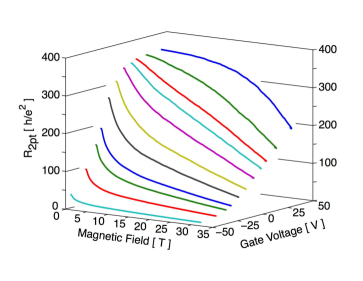
The hydrogenated graphene devices were mounted on ceramic carriers, in turn mounted on G10 sample holders, that were then mounted to either a pumped 4He or 3He refrigerator. The samples were cooled in either the gas or liquid phase of helium. Preliminary characterization was performed with a 9 T solenoid (McGill). All electrical measurements on hydrogenated graphene were performed using standard lock-in techniques at 13 Hz and at a low current excitation nA. Gate voltage was applied with a DC voltage source, and gate leakage current was monitored for all measurements with a DC ammeter. The gate leakage resistance was at minimum . High-field measurements were performed on samples using the both a 33 T resistive magnet and the hybrid superconducting-resistive magnet of the NHMFL facility in Tallahassee. With the hybrid system, a DC magnetic field of 45 T was applied normal to the graphene surface with a superconducting outsert coil generating up to 11.5 T, and an additional 34 T field generated by a resistive insert magnet. Colossal negative magnetoresistance was observed in five distinct samples, with the resistance versus magnetic field and gate voltage of sample #HG18 given in Fig.6.
References
- (1)
- (2) A. Guermoune et al., Carbon 49, 4204 (2011).
- (3) U. Bischler and E. Bertel, J. Vac. Sci. Tech. A 11, 458 (1993).
- (4) A. Jorio et al., Raman Spectroscopy in Graphene Related Systems, Wiley-VCH, Singapore, 2011.
- (5) M.M. Lucchese et al., Carbon 48, 1592 (2010).
- (6)