Relaxation of excited spin, orbital, and valley qubit states in single electron silicon quantum dots
Abstract
We expand on previous work that treats relaxation physics of low-lying excited states in ideal, single electron, silicon quantum dots in the context of quantum computing. These states are of three types: orbital, valley, and spin. The relaxation times depend sensitively on system parameters such as the dot size and the external magnetic field. Generally, however, orbital relaxation times are short in strained silicon ( to s), spin relaxation times are long, ( to 1 s), while valley relaxation times are expected to lie in between. The focus is on relaxation due to emission or absorption of phonons, but for spin relaxation we also consider competing mechanisms such as charge noise. Where appropriate, comparison is made to reference systems such as quantum dots in III-V materials and silicon donor states. The phonon bottleneck effect is shown to be rather small in the silicon dots of interest. We compare the theoretical predictions to some recent spin relaxation experiments and comment on the possible effects of non-ideal dots.
I Introduction
The spin of an electron in silicon may act as an information carrier in future information technologies, from quantum computers to spintronics. For quantum information applications, the spin of cold, localized electrons in silicon can make a qubit with a low memory-error-rate due to the purifiability of the spin environment (a spin-0 nuclear isotope is available) and silicon’s inherently weak spin-orbit interaction, which isolates information stored in the electron spin from charge movement and other noise. Quantum dots, in addition, allow for ready tunability and alignment of the confined electron (for physical transport, computation via qubit-qubit coupling, readout, initialization) Friesen et al. (2003), the potential for a fabrication route with present-day lithographic techniques, and the enabling of a fast, DC-controlled two-qubit gate based on Heisenberg exchange Loss and DiVincenzo (1998). The goal of designing and constructing quantum computers based on quantum dots requires characterization of all their physically relevant properties. For this, it is necessary to have a full toolbox of experimental diagnostics - in this case, one electron excited-state lifetime measurements as a function of external parameters such as temperature and magnetic field, and to be able to interpret these measurements in the light of theory.
In this paper we present calculations of the dominant spin relaxation processes in ideal silicon quantum dot spin qubits Tahan (2005) along with calculations for orbital and valley relaxation. Our particular emphasis is decay due to phonon coupling, since this mechanism is believed to be responsible for across wide parameter regimes relevant to quantum information applications. We will indicate in detail how it can be distinguished experimentally from other mechanisms.
A full, experimentally verified theory of the energy relaxation processes of the excited electronic states in silicon quantum dots is important for several reasons. First, it accomplishes a major step on the experimental path to determining the quantum coherence times of isolated spins in silicon (a preeminent goal in the verification of a qubit). Second, it helps corroborate our understanding of the material system and better characterizes the device under scrutiny; an example would be transport spectroscopy of nearby energy levels and their line widths. Third, it provides necessary parameters needed for the design of future experiments, systems, and architectures. Indeed, if the dominant spin qubit relaxation mechanisms are as we predict, we can not only validate the lifetimes of silicon qubits, but also retrieve the relative magnitudes of the dominant spin-orbit coupling contributions inherent in the device (important for both silicon quantum computing and silicon spintronics applications), as well as the nature and energies of the various states above the two spin-qubit states. Finally, the lifetimes of excited orbital states are relevant to optical pumping schemes, many-phonon decoherence calculations, transport spectroscopy, beyond single-spin qubit implementations Smelyanskiy et al. (2003); Shi et al. (2012), and other areas of quantum control.
It has long been known that localized spins in silicon can have exceedingly long lifetimes, even at relatively high temperatures ( 2K) Feher and Gere (1959). Theoretical predictions of spin decoherence times are notoriously difficult as many mechanisms can relax a spin, even in the more robust case of direct energy relaxation, or processes, where a quantum of energy is lost to the environment. In silicon, for example, energy relaxation processes may depend on the many-valley nature of the conduction band electrons; neglecting this effect leads to incorrect predictions (to many orders of magnitude) Pines et al. (1957); Abrahams (1957). The key realization came in 1960 from Roth Roth (1960, ) and, independently, Hasegawa Hasegawa (1960) - that spin mixing to the (1s-like) valley manifold states explains the “fast” relaxation observed for donor electrons. Soon after, Feher, Gere, Wilson et al. Feher and Gere (1959); Wilson and Feher (1961) and Castner Castner (1963, 1967) thoroughly fleshed out the experiments and theories of donor state lifetimes in silicon. Castner was the first to calculate relaxation across different valley donor states. This body of work was the basis of some of the first proposals for electron spin qubits in silicon as a basis for a quantum computer Kane (1998). This reinvigoration of the field has led to the extension of these original relaxation theories to new nanostructures like donors and quantum dots in strained silicon Tahan et al. (2002); Tahan (2005); Glavin and Kim (2003) and in III-V quantum dots Khaetskii and Nazarov (2000, 2001).
The region of qubit interest in our case refers to a spin qubit with finite magnetic field, well below any degeneracy with higher orbital or valley states. We can summarize the key results of this paper and prior work on qubit relaxation relevant to qubit and quantum computer design in silicon quantum dots as follows:
-
1.
We are concerned with the lifetimes of excited states of a 0-dimensional (0D) localized electron in silicon. The relaxation of 1D and 2D mobile electron spins has been investigated for spintronics applications. This has led to some misconceptions about electron spin relaxation in 1D and 2D vs. 0D. They are in fact very different. For mobile electrons, scattering plays the key role Glazov (2004); Tahan and Joynt (2005), and spin rotation between or during scattering events is the driver of loss of spin memory (D’yakonov-Perel and Elliott-Yafet effects Zakharchenya (1984)). This normally leads to spin lifetimes on the order of microseconds in silicon Tyryshkin et al. (2005); Tahan and Joynt (2005). Since scattering is not an issue in 0D, this is an unjustified worry for spin qubits for silicon quantum computers. However, spin lifetime measurements in silicon quantum wells can help determine relevant spin-orbit coupling parameters needed for quantum spin relaxation calculations.
-
2.
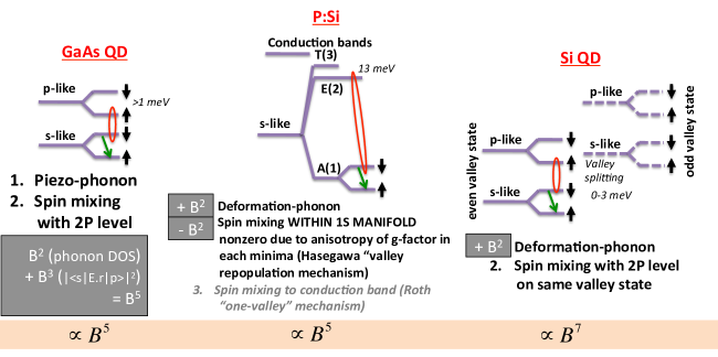
Spontaneous emission of a phonon is the dominant mechanism determining the spin-flip time, ( being the characteristic time for true energy relaxation to the environment via a phonon or photon), at temperatures around 100 mK. Photon emission is negligible because of the much lower density of final photon states. Phonon emission accompanied by a spin-flip occurs due to spin-orbit mixing within the crystal. Of the “bulk” Roth Roth (1960) and Hasagawa Hasegawa (1960) mechanisms that are relevant for donors in unstrained silicon, the “valley repopulation” mechanism disappears with increasing [001] strain as is common in silicon quantum wells Tahan et al. (2002). The “one-valley” mechanism goes to zero if the magnetic field is parallel to one of the three crystallographic axes, and goes as for other directions Glavin and Kim (2003).
-
3.
The effect of germanium in a SiGe QD heterostructure is not significantly detrimental to relaxation times for growth-typical Ge concentrations Tahan et al. (2002) (in the virtual crystal approximation).
-
4.
The spin-orbit coupling (SOC) in lateral Si quantum dots comes predominantly from structural inversion asymmetry (SIA) and symmetry-breaking due to interface effects leading to both Rashba-like and Dresselhaus-like SOC terms Zakharchenya (1984); Nestoklon et al. (2006a, 2008); Prada et al. (2011). (The relative magnitude of Dresselhaus-like and Rashba-like SOC in silicon quantum wells or dots has yet to be verified experimentally, let alone systematically across samples.) Each term gives a characteristic magnetic field anisotropy in Overall, is proportional to the seventh power of the magnetic field Tahan (2005). This contrasts sharply with GaAs quantum dots and Si donor states. For these two cases (though for different reasons). The ratio of the Rashba-like and Dresselhaus-like terms are expected to be sample dependent since in silicon they are due solely to interface effects (silicon, unlike III-Vs, has no bulk-inversion asymmetry (BIA)).
-
5.
Direct coherent rotations due to nearby spins in the semiconductor are possible.
-
(a)
At zero and low magnetic fields, direct dipole-dipole magnetic coupling with the central electron qubit and other electrons in the environment can occur. These rotations are technically coherent processes, but they result in spin flips that change the longitudinal component of the qubit magnetization and thus appear like processes. These processes do not depend on and can set upper limits on observed times. The strength of this interaction is reduced as the inhomogeneity of the electron line widths increases, though even one electron spin exactly at resonance 200 nm away can cause 200 ms effective lifetimes. A full theory is beyond the scope of this paper.
-
(b)
At zero fields, direct electron qubit - nuclei flip-flops are possible leading to -like rotation. At finite fields this mechanism is suppressed due to the mismatch of the electrons and nuclei respective g-factors.
-
(c)
These mechanisms may in some cases be corrected via spin-echo techniques or suppressed by freezing out the background spins
-
(a)
-
6.
Other mechanisms for longitudinal spin relaxation, , such as hyperfine coupling to Si29nuclei in natural Si, 1/f noise, and Johnson noise, are estimated to be small in the parameter ranges considered here, though further work is required to verify this. The magnetic field dependence of these effects allows them to be distinguished from spin-phonon coupling.
-
7.
The phonon bottleneck effect operates rather weakly in the parameter regime of interest for quantum dot applications. It can be calculated in a theory that goes beyond the electric dipole approximation; the result is only a slight enhancement of
-
8.
Orbital relaxation in strained silicon is much faster than in bulk silicon in some important cases. Surprisingly, the rate of spontaneous decay from the first excited orbital state in silicon quantum dots can be comparable to that of GaAs quantum dots, which are commonly expected to relax more efficiently due to that crystal’s piezoelectric nature. This has important implications for optically-induced motional spin-charge transduction (readout) and optical pumping (initialization) of spin qubits Friesen et al. (2004), making the former harder and the latter easier, as well as for excited state spectroscopy.
-
9.
Excited valley state relaxation can be slow in silicon due to a small matrix element connecting valley states of different symmetry; this leads to the hope of valley qubits Tahan (2004, 2003); Smelyanskiy et al. (2003). The phonon emission rate has a maximum at the Umklapp phonon energy (11 meV and 23 meV for transverse and longitudinal phonons in silicon) that connects valley minima from one Brillouin zone to its nearest neighbor Castner (1963). This leads to—at the longest—nanosecond relaxation times Soykal et al. (2012) in P donors with their large valley splitting (~10 meV), but in quantum dots is suppressed due to a large energy mismatch. However, the valley index in general cannot be considered a good quantum number in quantum dots due to large valley-orbit mixing Friesen and Coppersmith (2010). For the same reason, “valley relaxation” in realistic devices can be dominated by orbital relaxation due to mixing with nearby orbital levels. The situation is different and more favorable in some cases such as for Li donors Smelyanskiy et al. (2003); Soykal et al. (2012).
- 10.
This content is arranged as follows. We begin with an introduction to the single electron states in silicon quantum dots typical of heterostructures used for qubits today. We follow with a discussion of the electron-phonon interaction, the dominant relaxation mechanism in these devices. We then use that theory to calculate the orbital relaxation (no spin flip) of low-lying excited states to states having the same valley index. We do this first using the electric-dipole (ED) approximation and then including all multipoles. This gives useful numbers for excited orbital state lifetimes as well as a quantitative idea of the extent of validity of the ED approximation in further calculations. Then the main subject of this paper is tackled, namely the spin flip mechanisms relevant to quantum dots. In this section, we review and adapt the previously known “bulk” spin-flip mechanisms to the quantum dot case. We then consider new mechanisms due to structural inversion asymmetry which give the dominant spin relaxation mechanisms for most of the magnetic field range. This is followed by comparisons with spin relaxation mechanisms (noise, nuclei) and valley relaxation, which completes the narrative of excited lifetimes in single electron quantum dots relevant to quantum computing. Where possible we compare the results for quantum dots with those for P donors in silicon and GaAs quantum dots, both of which are relevant reference systems.
The final section summarizes the relation of theory to experiment. It is difficult to make sharp predictions for the absolute magnitude of because of strong dependences on quantities that are usually somewhat uncertain, particularly the dot size, as well as a reliance on bulk material constants which may vary in nanostructures. We show how to overcome this problem by combining measurements of qubit spin lifetimes with measurements of excited orbital state energies and lifetimes. It is precisely for this reason that we deal in such detail with the excited states.
II Silicon Quantum Dot states
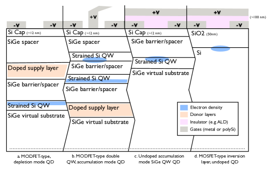
This work is concerned mainly with lateral quantum dots formed by heterostructure confinement in the growth () direction and lateral confinement by metallic top gates. Figure 1 shows some of the heterostructure choices possible in constructing these dots, from modulation doped two-dimensional electron gas (2DEG) structures depleted by top gates to accumulation mode inversion layer devices in MOSFET-like structures. We will concern ourselves here predominately with the SiGe QW QD case, although our considerations should carry over to Si MOSFET dot structures as well.
In semiconductors, the electron wave functions are superpositions of Bloch states at the bottom of the conduction band (CB), so the indirect band-gap, “many-valley” nature of silicon (as opposed to a single -valley in GaAs) takes on great importance. In a biaxially-strained silicon QW, the number of states is doubled relative to GaAs, but reduced from the 6-fold degeneracy of electrons in the bulk. The conduction band (CB) minima located at with have band energies lower than the minima at and by about 0.1 to 0.15 eV at typical strain values (20-30% Ge in the barriers) Schaffler (1997). Thus the valleys are populated but not the and valleys Yu and Cardona (2001). A similar splitting is at work in Si MOSFET-type structures, though here the physical origin of the lifting of the degeneracy is due to anisotropy of the silicon effective mass (and in some cases local strain). In the absence of magnetic fields and valley-splitting effects, the electronic ground state in this system is four-fold degenerate (spin and valley). When potentials or boundary conditions that mix the two valleys are present, as they always will be to some extent, there will be excited valley states corresponding to different linear combinations of the valley minima. So each valley state has its own identical set of orbital and spin states and an additional quantum number is needed to specify which valley state the electron occupies.
A magnetic field splits the degeneracy of the spin states. The valley degeneracy is split by the hard confinement of the QW interfaces (or the impurity potential in that case) and is influenced by a number of parameters, especially the magnitude of the electric field in the growth direction and the sharpness of the confining potential. For the moment, we assume for simplicity that any static magnetic field is small or directed in the plane of the QW (so that the orbital functions are unperturbed) and that the well walls, located at are smooth. In these circumstances, we may write
is the envelope function obtained by solving the confinement problem in the effective mass approximation for the -th orbital, are the coefficients weighting the two valleys for the -th valley state ( for strained silicon, for bulk silicon), and are the lattice-periodic parts of the Bloch functions, , at the conduction band minimum . for the symmetric valley (“sin-like”) state and for the antisymmetric valley (“cosine-like”) state. It is often convenient to expand the Bloch functions into a sum,
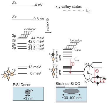
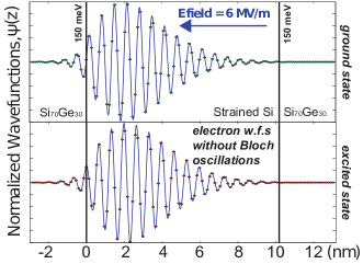
where weight the Fourier components of expansion (independent of ) and are the reciprocal lattice vectors. The wave functions for a more realistic device, calculated in the tight-binding theory of Ref.Boykin et al. (2004), are shown in Figure 8 (where the “Kohn-Luttinger” oscillations are evident but the lattice periodic oscillations are not included). A donor vs. dot energy level comparison is shown in Figure 2.
Until now we have only concerned ourselves with “perfect”(completely flat) interfaces. In these cases the valley and orbital states are well defined - valley index being a generally good quantum number - much like the isolated donor case. In reality most interfaces are imperfect; they have alloy disorder (Si vs. Ge atoms), steps due to miscut, steps due to growth layer formation, and even interface states and traps (especially with respect to Si/SiO2 interfaces). This leads to mixing of the valley and orbital wave functions as well as diminishing of the valley splitting (due to interference) Friesen et al. (2007); Friesen and Coppersmith (2010), and as such, wave functions and splittings that vary from device to device and dot to dot. These microscopic variations are not considered in this paper. Fortunately, these effects are often not large corrections to the calculations below, as the experimentally accessible energy splittings come into the equations at a much higher power than the relevant (experimentally inaccessible) matrix elements. As we go we will point out differences from our theory for the ideal and likely situations, focusing on experimentally accessible signatures.
III Electron-Phonon Interaction
Phonons are quanta of lattice vibrations, that is, mechanical motion that gives time-dependent stress. This alters the band structure by shifting band energies and lifting degeneracies Ridley (1999); Yu and Cardona (2001). It is typically assumed that this effect does not change the band curvature (effective masses) but does shift the energy states of interest. The shift in energy of the band edge per unit elastic strain is called the deformation potential and is common to all semiconductors and solids. In polar crystals, distortion of the lattice can also create large internal electric fields which affect the electron. This is the piezoelectric interaction. Ionic crystals like GaAs suffer from piezo-phonons, which are often very efficient at electron scattering; silicon, being non-polar and centrosymmetric, has none. While optical strain also exists in materials with two atoms per unit cell, such as silicon, optical phonons in silicon have a narrow bandwidth centered at a much higher energy than a quantum computer would operate. We briefly review the theory of the electron-phonon deformation potential interaction outlined by Herring and Vogt Herring and Vogt (1956).
| Constant | Value |
|---|---|
| C | |
| J s | |
| m/s | |
| C2/Nm2 | |
| 11.8 | |
| (Si) | 1.999 |
| (Si) | 1.998 |
| (Si) | 8.77 eV=1.4 J |
| (Si) | 5 eV=8 J |
| (Si) | 2330 kg/m3 |
| (Si) | 9330 m/s |
| (Si) | 5420 m/s |
| (Si) | 0.543 nm |
| (Si) | |
| 1.38 J/K |
The energy shift of a non-degenerate band edge due to strain is given by
| (1) |
where
is the strain tensor and is the deformation potential tensor for the th silicon CB valley. Since our electron is confined to massively strained [001] silicon, we need only include the valleys which have deformation potential tensors given by
| (2) |
where relates to pure dilatation and is associated with shear strains. is a unit vector in the direction of the th valley. For silicon under compressive stress along [001], opposing valleys move in energy identically. In order to associate phonon modes with strain, we can expand the unit cell displacement in plane waves,
destroys a phonon with wavevector q and polarization (2 transverse and 1 longitudinal; see details in Table 2) of a phonon; is its unit displacement vector. This results in a strain tensor due to a phonon of
| (3) |
The operators and have matrix elements
is the mass of the crystal and is the phonon occupation number of the mode with wave number and polarization . The complete electron-phonon Hamiltonian must be summed over phonon modes and polarizations. For a [001] strained-silicon quantum well, it can be written succinctly as
| (4) |
We are especially concerned with the anisotropic effects due to the massive strain of the system in question. As can be seen from Eq. 2 and the deformation constant values in Table 1, the shift in energy of a specific valley due to an acoustic phonon is very anisotropic. In the case of bulk Si, the six conduction band minima are equidistant from the -point and thus form an isotropic response to phonon deformations. This means essentially that transverse phonons will not contribute to the relaxation times for intervalley transitions of the same symmetry (that is, for initial state and final state ). Another way to see this is to consider the electron-lattice matrix element between different plane wave states at the same minimum (Equation 3.29 of Ref. Hasegawa (1960)),
where . We have used the polarization index to indicate a transverse phonon. The matrix element between two dot wave functions is then
It’s easy to see from the above equation that if is proportional to the identity matrix (assuming ), then the transverse phonon matrix elements must be zero since . The point is that in strained silicon, only the minima are occupied so unlike the bulk silicon case, transverse phonons will contribute. This turns out to be very important in relaxation calculations, as will be seen below.
| Longitudinal | Transverse | Transverse | |
|---|---|---|---|
| 0 |
IV Orbital Relaxation in Strained Si Quantum Dots
The line widths and characteristic behavior (dependence on magnetic field, etc.) of the lowest lying excited states in quantum dot systems are usually very relevant for characterizing a spin-based qubit. We begin by considering the relaxation of an excited state that involves no spin flip and takes place within the same valley state (assuming for now no valley-orbit mixing). Spontaneous emission of a single acoustic phonon is the dominant relaxation mechanism for excited electronic states in Si at QC temperatures (100 mK) (an ansatz guided by empirical evidence for silicon donors Feher (1959); Feher and Gere (1959) and GaAs quantum dots Hanson et al. (2007)). The deformation potential approach Herring and Vogt (1956) is easily modified to include strain Tahan et al. (2002). The phonon-induced energy shift is very anisotropic for a silicon conduction band valley. Because of this the results for strained silicon are quite different from those of bulk silicon Abrahams (1957).
In the bulk, the six conduction band minima are equidistant from the -point and thus form an isotropic response to phonon deformations (specifically the case where for all across both states). So the angular integral over transverse phonons averages to zero. For example, the transition from the ground, 1s-like symmetric state to the 2p-like, symmetric state in bulk silicon has no transverse phonon contribution Abrahams (1957). The same transition in strained silicon does have such a contribution, because the cubic symmetry of the six minima has been broken by strain, and indeed it is the largest term. This greatly increases the relaxation rate since the inverse sound velocity comes into the rate equations with a very high power as we will now show.
Fermi’s Golden Rule, between states of arbitrary spin,
| (5) |
is the basis for our phonon relaxation rate calculations. Here, is the state of the electron in the dot on level with spin state and on valley manifold , including the effect of a magnetic field. We assume an isotropic phonon spectrum such that the energy of the phonon is , where and is the velocity of the mode Setting for orbital relaxation without a spin-flip and , is the energy splitting between states and , is the electron-phonon interaction of Eq. 4. Summing over phonon modes, using and (see Table 2) for the wave vector and polarization vectors and using the electric dipole (ED) approximation, , we find for the phonon-induced relaxation rate,
| (6) |
where
| (7) | ||||
the matrix elements are , is the mass density of Si, is the energy gap between orbital states, and are the longitudinal and transverse sound velocities. The single electron envelope functions can be calculated by solving the Poisson and Schroedinger equations directly as in Ref. Friesen et al. (2003) or, as is normally done, by approximating the potential as a parabola, giving harmonic oscillator states defined by the fundamental energies . With the envelope functions and , the matrix element is given by
| (8) |
where is the lateral size of the dot, , and and are the dot sizes in the and directions. We define . Thus, the orbital relaxation rate from the lowest orbital state for a slightly asymmetric (non-degenerate excited state), parabolic dot is
| (9) |
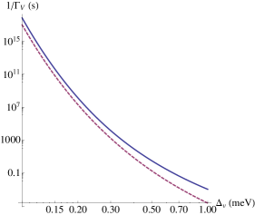
(we have used the fact that to eliminate terms due to longitudinal phonons). Because appears in the fifth power (general case) or fourth power (parabolic dots) in Equations 6 and 9 for orbital relaxation, an accurate value for is much more important than equivalent accuracy in the wave function matrix elements. The dipole approximation is valid until roughly ( is the maximal linear size of the dot) when the relaxation rate starts to decrease due to phonon bottleneck effects. We treat this effect explicitly in the next section.
V Phonon Bottleneck Effect
When the dot becomes very small ( comparable to a few interatomic spacings), the relaxation rate is reduced. This is due to the impossibility of satisfying simultaneously energy and momentum conservation during an electron-acoustic-phonon scattering event Benisty (1995). Mathematically, the phonon bottleneck effect is due to the fast oscillating exponential factor: emission of a phonon with wave vector is unlikely when Benisty et al. (1991). Table LABEL:cap:Phonon-bottleneck-numbers charts this transition for parabolic Si quantum dots. Note that in a lateral quantum dot, unlike excitonic quantum dots, Auger processes and electron-hole scattering do not play a role in negating phonon bottleneck. Assuming parabolic dots, only dots with fundamental energies meV are small enough (and virtually impossible to construct with laterally-gated devices) for phonon-bottleneck effects to make a significant impact on increasing the orbital relaxation times.
| (meV) | (nm) - Si | (nm) - Si() | (Eq. 6) | (Eq. 10) |
|---|---|---|---|---|
| 0.05 | 127 | 447 | s | s |
| 0.1 | 90 | 223 | s | s |
| 0.2 | 63 | 112 | s | s |
| 0.3 | 52 | 75 | s | s |
| 0.4 | 45 | 56 | s | s |
| 0.5 | 40 | 47 | s | s |
| 1 | 28 | 22 | s | s |
| 2 | 20 | 11 | s | s |
| 3 | 16 | 7.4 | s | s |
| 8 | 10 | 2.8 | s | s |
| 10 | 9 | 2.2 | s | s |
We outline the calculation for Si, including the valley effects, in Appendix IX.1. The chief difficulty is to include all multipole moments. The result is that the orbital relaxation rate for a parabolic dot (in all three dimensions) from its first orbital, excited state to its ground state is given by
| (10) |
where is the size of wave function in the growth direction and , . The coefficients are defined by
The results are plotted in Figure 3. Note that the exact expression, Eq. 10, reduces to the dipole approximate expression, Eq. 6, when as expected. For large the exact solution for the orbital relaxation rate begins to diverge from the electric-dipole approximation early on and never falls below a picosecond or so. Despite this, the electric-dipole approximation holds well for small energy gaps, meV, where a quantum computer in silicon will most likely operate. This figure shows that there is no significant benefit in going beyond a few meV. Only around 10 meV does the relaxation time start to increase, but this a relatively small effect. It does demonstrate, however, that the phonon bottleneck effect may be experimentally observable in these systems and, more importantly, that our use of the electric-dipole approximation gives results below for the spin-flip times that may be considered a lower bound on the maximum possible time .
Table 3 compares the output of Eq. 6 and Eq. 10 for pure orbital relaxation in lateral silicon quantum dots. One can compare these results to those for GaAs quantum dots Fujisawa et al. (2002), where typical values would be s for meV and piezo-phonons dominate. Excited orbital states in strained silicon typically relax in nanoseconds or faster, corresponding to a level broadening of a micro-eV or wider. It is possible that a low-lying excited valley state (of the same spin direction) may be closer in energy than the orbital level. For bulk silicon, theory and experiment have found characteristic relaxation times for the - transition of ~200 ps Greenland et al. (2010).
VI Spin-flip () times
Our expressions for orbital relaxation in strained silicon can be extended to the case of a spin-flip transition due to spin-orbit coupling (SOC) in a QW. We expect that relaxation via a phonon is the dominant cooling mechanism, in this case mediated by SOC which mixes pure spin states. This is known to be the case for donor-bound spins in bulk Feher and Gere (1959). Structural inversion asymmetry has traditionally been thought to be the dominant source of SOC in silicon quantum wells due to the large electric field common to modulation-doped or top-gated SiGe heterostructures. The nature of this SOC has been well described elsewhere Winkler (2003); Tahan and Joynt (2005); Nestoklon et al. (2006a, 2008); Prada et al. (2011); it leads to a Rashba term in the Hamiltonian of the electrons. However, interface effects that break the inversion asymmetry can also lead to a generalized Dresselhaus-like term Nestoklon et al. (2008). Surprisingly, this can lead to effects of similar or even greater magnitude than the Rashba term Nestoklon et al. (2006a, 2008); Prada et al. (2011). We discuss this further below. Here we only note that the zero-field energy level splittings caused by SOC are small, of the order of eV, which validates our use of a perturbation theory that uses zero-order electron wave functions and energy levels taken from the SOC-free Hamiltonians.
Until the appearance of Refs. Friesen et al. (2004); Tahan (2005), there was no finite spin-flip time prediction for lateral silicon quantum dots when the external field is parallel to . Previous theories for in silicon had been based on the two dominant mechanisms relevant to P:Si donors: the “valley-repopulation” mechanism (bulk SOC mixing with the six nearby 1s-like states) and the “one-valley mechanism” (bulk SOC mixing with continuum states) Hasegawa (1960); Roth (1960, ). Both mechanisms are independent of the size and shape of the localized electron wave function. We showed rigorously in Ref. Tahan et al. (2002) that the former becomes negligible with [001] strain. The latter is slightly modified with strain and goes to zero for certain directions of the static magnetic field, particularly the [001] direction (the most relevant to QC), for both one and two-phonon processes Glavin and Kim (2003). We review these bulk mechanisms here as they are relevant for donor qubits and in some cases may be seen as residual mechanisms at low magnetic fields in dots. Then we will derive the spin relaxation times for dots in strained structures due to inversion asymmetry-based SOC leading to a that is finite for parallel to
VI.1 Bulk spin-flip mechanisms
For donor states in bulk silicon, Roth and Hasegawa Hasegawa (1960); Roth (1960, ) identified two mechanisms that have been confirmed experimentally up to 2 K in P donor spins Wilson and Feher (1961). The spin relaxation in the Roth-Hasegawa picture is due to a modulation of the system’s g-factor by acoustic phonons. Both mechanisms are direct single-phonon processes. The g-tensors for a given conduction band state can be written as a sum over the g-tensors at each conduction band minimum,
where is the squared amplitude ("population" in the early literature) of the single electron wave function at the th valley and .
There are two mechanisms leading to spin flip. The “valley-repopulation” mechanism is due to mixing between the symmetric ground state of the donor electron and the split-off doublet state where a phonon changes the . The “one-valley” mechanism is due to phonon-induced modulation of the themselves and subsequent mixing with nearby conduction bands which are coupled through an inter-band deformation potential. The two mechanisms are of the same order of magnitude in the bulk case and complementarily explain the angular magnetic field dependence of in those systems Wilson and Feher (1961).
Ref. Tahan et al. (2002) showed how the valley-repopulation contribution to the spin-flip becomes negligible with increasing [001] compressive strain as is inherent in a silicon quantum dot. This can be seen easily qualitatively. Consider first a potential with spherical symmetry. The population amplitudes describing the lowest six conduction states are given by Wilson and Feher (1961):
in the valley basis . The six states are split even at zero strain by non-spherical central-cell corrections in the donor case (the sharp potential of the donor) and by the interfaces in the quantum dot case. SOC represented by the anisotropic g-factor mixes the singlet ground state only with one of the doublet states Tahan et al. (2002). In QDs the strong compressive strain in the direction causes a large relative splitting between the six valley states; the result is that only the and states will be populated. These symmetric and antisymmetric valley states are not mixed by the SOC which results in a vanishing matrix element. So, in the quantum dot limit ( valleys populated), the valley-repopulation contribution to the spin-flip rate becomes negligible. Note that for this mechanism we only consider mixing to the six lowest states of the donor, all of which have orbital s-like character. The states in a donor are typically meV (bulk) to meV ([001] strain) away. Mixing with these states will be considered separately below.
The one-valley mechanism, however, is relevant to QDs. Roth showed that in bulk silicon, the contribution from mixing with nearby bands is described by a Hamiltonian
where c.p. stands for cyclic permutations. Group theoretical considerations and perturbation theory lead to the conclusion that the dominant contribution to comes from mixing with the nearby and bands and is given by
where is the usual crystal spin-orbit vector, are the energy gaps to the relevant bands, and is the inter-band deformation potential. represents a sum over the six minima in the bulk case, but in a lateral quantum dot the dominant contribution comes only from the minima and was determined by Glavin and Kim Glavin and Kim (2003) to be
The constant was experimentally determined by Wilson and Feher Wilson and Feher (1961) as . The time due to can be readily calculated and is given by Glavin and Kim (2003)
where define the angle of the magnetic field relative to [001]. is the Bose function. It is evident that this equation produces infinite relaxation times if the magnetic field points along the [001] or [011] axes. Figure 4 plots the one-valley relaxation rate as a function of magnetic field direction. We particularly stress that the dependence of is the characteristic signature of this mechanism and that this rate is very small in general.
VI.2 Dot-specific mechanisms
Now we will consider SOC that comes from the dot structure itself. The spin-orbit Hamiltonian for a two dimensional electron is conventionally written as
where are the in-plane wave vector components; and are the strengths of the so-called Rashba and Dresselhaus spin-orbit terms. This, combined with electron-phonon coupling, can also produce spin relaxation, and the effect (with has been computed for GaAs QDs Khaetskii and Nazarov (2000). In Si QDs, there is SIA SOC that comes from the fact that the mirror symmetry is broken. This occurs in SiGe/Si/SiGe heterostructures and in MOSFET-type QDs either by modulation doping or by a top-gate induced electric field Tahan and Joynt (2005). In contrast, Dresselhaus SOC has traditionally been assumed to be absent in Si structures because bulk Si has inversion symmetry. It was recently shown Nestoklon et al. (2008); Prada et al. (2011) that this is not the case. The breaking of inversion symmetry by the interfaces gives a non-zero Dresselhaus-like term that can be surprisingly large Prada et al. (2011). This has yet to be verified experimentally. Often, experimental measures of spin relaxation involve terms proportional to so the terms are hard to verify independently. Therefore we will keep both terms in and compute the spin relaxation that comes from these asymmetry-induced effects. The results differ from those of the GaAs quantum dot analog due to the many-valley nature of silicon and the dominance of acoustic over piezo-phonons in silicon.
The orbital energy level splittings are much reduced in quantum dots relative to donors (see Figure 1) because of the more shallow potential. It is thus relatively easy to make the Zeeman splitting larger than the orbital splitting. However, for quantum computing the likely situation is for the Zeeman splitting to be less than the orbital splitting to maintain a good qubit manifold. Here we will consider only this case where the magnetic field splitting is small compared to the orbital splitting. We comment on this approximation further below. In Si, the Hamiltonian for the electron-phonon matrix element is, for :
where denotes a state with an electron in the th level of the dot with spin . Again, we consider relaxation processes within the same valley state. A phonon with wave vector and polarization is absorbed or emitted depending on whether or is the spin projection on the -axis, defined to be along the external applied field Hence etc.
The matrix elements of are
where is the dipole matrix element for the dot states, and , and where we have used the trick ; we use units with causes the eigenstates to be mixtures of up and down spin states. For example, if the unperturbed orbital ground states and are perturbed by , the new eigenstates and are
where is the transverse mass and we have expanded around with . The superscript indicates first order in - the spin-orbit splitting compared to the orbital excitation energies. It is important to compute the correction for reasons that will soon become apparent.
Our interest is in the matrix element
where the subscript indicates that there is a phonon in the final state. We find
and we make the electric dipole approximation which gives
Because , the overall matrix element is reduced by roughly . This is the manifestation of the so-called Van Vleck cancellation.
We do the thermal average over phonon states and apply Fermi’s Golden Rule. This yields
where
The integral is over the directions of ( and are not the same as and which give the directions of the magnetic field.)
Following Ref. Khaetskii and Nazarov (2001) we now define the dot polarization tensor
where the sum is over all the orbital states. The opposite valley states are not included in the sum since the intervalley electron-phonon coupling is assumed to be small (this could be different in non-ideal interfaces). It is also reasonable to neglect since the spatial extent of the wave function in the growth direction is small compared to (at least by a factor of 10). The result (with restored), is
| (11) |
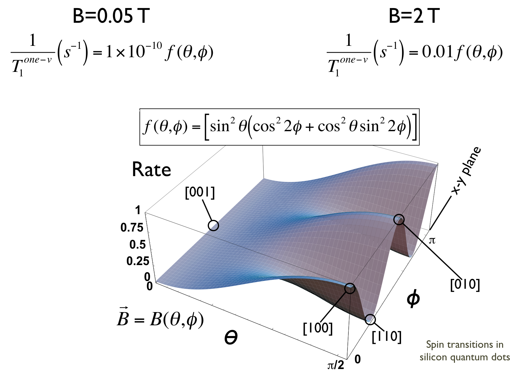
Note that we include a factor of two in the phonon population multiplier, , so to satisfy the traditional definition of where both relaxation and excitation are possible (although at very low temperature this term goes to one). The most striking qualitative feature of this expression is the dependence Tahan (2005); this can be considered as the characteristic feature of dot-specific SOC and contrasts with the dependence of bulk SOC, as well as GaAs quantum dots (which are dominated by piezo-phonon relaxation in energy regimes of interest Khaetskii and Nazarov (2001)). In addition, there is field anisotropy. To understand this anisotropy note that the diagonal elements are likely to dominate the off-diagonal elements and Examination of the expression then shows that the largest term in is proportional to This does not vanish when is along the -axis again in contrast to the Roth-Hasegawa contributions. If one wishes to determine and individually, then the smaller contribution proportional to must be measured. It could be enhanced if is very different from which would be the case for a very elliptical dot.
The polarization tensors (matrix elements) can be calculated numerically, or in the small magnetic field limit (where the first excitation energy is much less than the Landau energy), the zero B-field parabolic matrix elements can be used as a decent approximation. We can include the magnetic field in a circular dot explicitly if by utilizing the Fock-Darwin states L. Jacak (1998). In this case where is the fundamental energy of the dot, , , , , , and . Then, taking into account dipole selection rules (only transitions are allowed),
In the limit, with , reduces to and for an elliptical dot. To estimate the overall quantitative magnitude we shall assume a circular dot with a parabolic potential (note also that for a circular dot . Then with and and
| (12) |
where we have used
| (13) |
(for reference we find ). The contribution of longitudinal phonons is suppressed by roughly a fifth in and is neglected. For reference, the spin relaxation rate can also be written in terms of the dipole matrix elements between and , , as (assuming mixing to one excited state):
| (14) |
The magnitudes of and are material system and device specific. Wilamowski et al. Wilamowski et al. (2002) have measured eVcm = nm via 2DEG spin relaxation in Si/SiGe quantum wells. On the other hand, for a SiGe/Si/SiGe well and a field of (roughly a factor of 2 larger E-field than typical SiGe QW QDs but about right for SiO2 dots), Prada et al. Prada et al. (2011) theoretically find that and eVnm ; note that they mention that the term could decrease in (typical) heterostructure quantum wells with miscut, and that it will very from device to device. Calculations of the spin relaxation in 2DEGs Glazov (2004); Tahan and Joynt (2005) give assuming minimal cyclotron effects or ; so the two results are consistent if we attribute the Wilamowski result as due to . Nestoklen et al. Nestoklon et al. (2006b), also theoretically, find a value for roughly 6 times smaller than Wilamowski et al. Wilamowski et al. (2002) (, nm). Note that the measured line width in Ref. Wilamowski et al. (2002) does not depend on the in-plane orientation of the magnetic field, implying (at least for that device) that one SOC term dominates over the other Glazov (2004); Tahan and Joynt (2005).
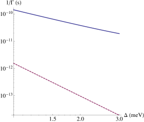
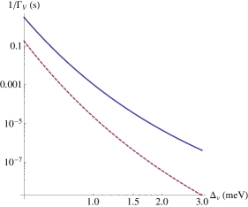
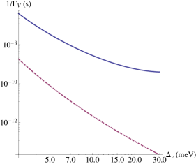
Figure 5 plots Equation 12 for as a function of orbital energy splitting using the result of Wilamowski et al., , and substituting values from Table 1. Also shown are some recent experimental results Hayes et al. ; Xiao et al. (2010); Simmons et al. (2011) which follow the trend but generally show longer lifetimes. We defer our comparison to experiment to the Discussion section below. Note that our results are for the electric dipole approximation, shown in the previous section to be a good approximation below ~1 meV. Calculations that attempt to calculate the spin relaxation beyond the dipole approximation Bulaev and Loss (2005); Raith et al. (2012) have shown the possibility of fast spin relaxation (“hot spot”) when the orbital and Zeeman energies are degenerate: a result of orbital-spin level mixing. This mixing is contingent on the nature of the SOC mixing — Dresselhaus (no mixing) or Rashba (mixing). Unfortunately we do not know the nature of the SOC in these devices and indeed it may depend on microscopic details and very from device to device (even on the same chip). An additional complication arises when the first excited state is a valley state or valley-like - a situation we will discuss later in the text. So a hot spot is not assured. Therefore, we mark these crossovers in energy in Figure LABEL:fig:Spin-relaxation-time as a possible position of interesting physics (fast relaxation) which may tell us more about the nature of these states. Our results are relevant for the quantum computing situation where and likely a good approximation beyond the crossing point (with the cyclotron modified wave function incorporated).
VI.3 Electrical and Magnetic Noise
Another possible mechanism that could limit in Si/SiGe quantum dots is the electric and magnetic noise coming from trapped charges and other two-level systems, noise in the circuitry, thermal and quantum current fluctuations in nearby conductors, etc. In this section we will point out how the presence of this sort of noise could be indicated by lifetime measurements, and how it can be distinguished from the other sources of noise we have been considering in this paper.
Electrical noise from a random field can produce spin relaxation if there is spin-orbit coupling present. Relaxation can occur by two distinct mechanisms: (1) spin-orbit-mediated virtual excitation to higher orbital states with spin flip and (2) modulation of the Rashba field. These correspond roughly to the Elliot-Yafet and D’yakonov-Per’el mechanisms in bulk.
For the first mechanism we have a Hamiltonian
This produces relaxation that is physically analogous to the spin-phonon mechanism, and the derivation is parallel, so we omit it. We obtain
where is the spectral density of the autocorrelation function, evaluated at the qubit operating frequency, and is a measure of the diameter of the dot. is a numerical factor of order one that depends on the shape of the dot. We write the applied field as is the z-axis of the lab frame. Note that, as before, the relaxation rate decreases as the excited state splitting increases since the spin mixing which allows the electric field to relax the qubit is via the excited orbital state.
The second mechanism is physically distinct in that it does not involve orbitally excited states; instead the noise is converted to random time-dependent effective magnetic field on the spin. It is sufficient to consider a Rashba Hamiltonian,
which leads to
where again is a geometry-dependent constant of order unity. Here, the rate increases with smaller dot sizes (). Reasonable values for the parameters are nm2 Prada et al. (2011) , and nm; evaluating this formula leads to
if is measured in V2-s/m Zimmerman et al. determined the strength of electrical noise in a Si SET structure by measuring fluctuations in the peak separations of Coulomb blockade oscillations, but so far this type of measurement has been peformed only at frequencies much less than 1 GHz, which makes it difficult to estimate the noise magnitude at typical qubit operating frequencies in real structures. But the only -dependence in comes from which is likely to vary extremely slowly with for any mechanism that one can think of. This means that defect-dominated electrical noise can be easily distinguished from other relaxation mechanisms by the fact that it is -independent.
Magnetic noise from quantum and thermal current fluctuations in metallic portions of the circuit will produce a fluctuating magnetic field at the qubit that can relax the spin. No spin-orbit coupling is required for this mechanism to operate. This effect has recently been calculated by Langsjoen et al. Langsjoen et al. (2012). These authors found values of of order seconds for typical quantum dot architectures. The field and temperature dependence is given by which reflects the photon density of states and the Bose function. The field and temperature dependences are again distinctive.
VI.4 Spin relaxation due to nuclei
Hyperfine coupling of the electron spin to nuclei can give a very small admixture of the opposite spin state into a predominantly up or down state. This mechanism would give a that depends relatively weakly on field. However, theoretical estimates give a small magnitude for this effect Wilson and Feher (1961); Khaetskii and Nazarov (2001); de Sousa (2003). This conclusion would of course be strengthened in isotopically purified Si28. Furthermore, this mechanism is not specific to dots and should occur also in donor spin relaxation, where s for Si:P at T and Feher and Gere (1959); Wilson and Feher (1961). It does not seem to have been observed. Hence this mechanism is probably negligible at the fields and temperatures under consideration here.
VI.5 Two-phonon processes
At higher temperatures there is an activated two-phonon contribution from SOC mixing in silicon quantum dots. In the Si:P system, these Orbach processes dominate for T 2K Tyryshkin et al. (2003). We can use the methods proposed by Castner Castner (1967) to estimate the Rashba + Orbach spin relaxation path. We arrive at
where we estimate for a circular dot that as the spin-mixing of the two states and is the orbital relaxation time of the first excited state. For a circular dot with a parabolic potential
| (15) |
Thus the temperature dependence of at higher temperatures can give an accurate measure of a technique already used to find energy splittings of donor states. This can provide a check on transport spectroscopy determinations of this quantity.
VII Valley relaxation
Electrons in lateral silicon quantum dots typically reside in the two degenerate conduction band minima along the direction. This doubles the number of levels in the dot relative to the -point-centered, direct band-gap III-V quantum dots as was described in Section II. Here we wish to consider the relaxation times of these excited valley states as we have done for low-lying orbital and spin states above. Castner was the first to calculate the relaxation across different valley states from the to levels in donors Castner (1963). This has been repeated in Ref. Smelyanskiy et al. (2003) for Li donors and for P and Li in strained silicon in Ref. Soykal et al. (2012). A similar calculation can be done for lateral quantum dots where the interface in is assumed perfectly flat and smooth, and thus the valleys can be considered good quantum numbers in the usual Kohn-Luttinger approximation (and the problem is separable in the three dimensions). We first consider this ideal (or “1D”) case (which may be relevant in some experimental situations) and then comment on the more usual case of significant valley-orbital wave function mixing due to imperfect interfaces.
 |
 |
 |
 |
 |
 |
VII.1 Ideal (1D) interfaces
We are concerned with relaxation across the same orbital and spin states but between valley states () in a silicon quantum dot, particularly the relaxation of the lowest excited valley state with no change in spin or orbital number (type 3 in Figure 2). Our approach to valley relaxation follows the same procedure as exact orbital relaxation (Section V and Appendix IX.1), where in this case we replace the matrix element with the inter-valley matrix element:
Assuming no valley-orbit mixing with higher states (separable wave functions in (, ) and ), the wave function for an electron in a lateral silicon quantum dot reads
where is the location of the minima along the -axis, (though these may be complex in the general case), and we have expanded the Bloch function in reciprocal lattice vectors, or , The first five terms of the Bloch expansion contribute 90% of the wave function amplitude (values from a recent study are listed in Table 1 of Ref. Saraiva et al. (2011)). Here, the envelope functions of the two states are the same, the spin states are the same, but the Kohn-Luttinger oscillations are out of phase (see Figure 8). We assume that the wave function consists of Gaussians in all three dimensions. Following our exact orbital relaxation calculation, the valley relaxation rate of a parabolic, circular quantum dot in a [001]-strained silicon quantum well is
| (16) |
where
and
where is the valley splitting, is the extent of the wave function (assumed gaussian) in and is the phonon wave length of the emitted Umklapp phonon, . The details of this calculation are given in Appendix IX.2.
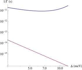
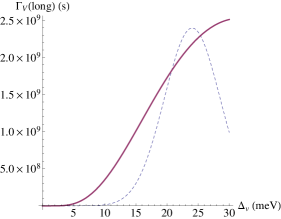
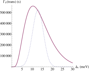
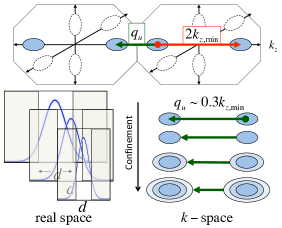
Let us compare Eq. 16 to pure orbital relaxation, Eq. 10. At first glance, the valley relaxation rate has a dependence as opposed to a in the orbital case (assuming parabolic dot potentials for both and matrix elements given due to gaussian wave functions). To understand this remember that for valley relaxation this transition occurs within the lowest manifold (both initial and final states have the same -like envelope function) such that the matrix elements . In the orbital case, we must calculate matrix elements from -like to -like states, such that . The valley relaxation expression also includes prominently a prefactor absent in the exact orbital case (Eq. 10). This prefactor predicts that the phonon relaxation rate will be peaked at the Umklapp phonon energy (assuming is constant with , which it isn’t). Equation 16 also shows the importance of the extent of the wave function; decreasing increases the relaxation rate. These effects are related, in that Umklapp phonons at which connect valleys in neighboring Brillouin zones are the most efficient relaxation channel (see Appendix IX.2 for more details). Figure 7 explicitly shows the valley relaxation rate in the two cases of fixed wave function height and wave function height that changes accurately with electric field and valley splitting. It turns out that the Bloch coefficients to the nearest valley at are most efficient and phonons are then emitted in the direction. As gets compressed, not only does the valley splitting increase due to interface scattering (approaching the “critical” Umklapp phonon energies at 13.4 meV (longitudinal) and 23.2 meV (transverse)), but the wave function gets broadened in momentum space, allowing lower energy phonons to connect the two opposite valleys (see Figure 9). So Umklapp valley relaxation is possible even at valley splittings smaller than . This effect causes the relaxation rate to continually increase as the valley splitting approaches , while the other “typical”exponentials kick in at higher splittings to cause a bottleneck effect as in the orbital case. The line width should be weakly dependent on the size of the dot in the lateral dimensions (as is the valley splitting) and much more so dependent on changes in extent of the wave function.
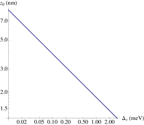
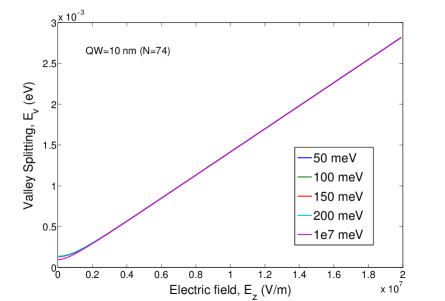
The valley splitting varies roughly linearly with E-field in a perfect quantum well where the electron only sees one side of the quantum well. Figure 7 shows the valley relaxation for an ideal interface as a function of valley splitting with a that changes correctly with We account for the change of wave function size in as a function of valley splitting. We take the ideal theoretical maximum valley splitting as (given in J)
where (V/m) is the electric field in the -direction, is the conduction band offset, (in eV m with in eV) Friesen and Coppersmith (2010). Thus, the valley splitting depends on the -field, which also determines the extent of the wave function in . now is a function of the E-field in (which varies by device and can often be changed somewhat in a single device). For this we define the wave function in as (assuming a triangular potential):
where (in meters). Now we replace with (in V/m). is the Airy function. So the extent of the wave function in, , changes with the valley splitting as:
For completeness, we may also look for an expression for the valley relaxation in the electric-dipole approximation. A reasonable approximation is to set in Equation 16 which, to leading order for a parabolic potential in all three dimensions, gives
| (17) |
The exact and approximate valley relaxation times are compared in Figure 10.
VII.2 Comments on imperfect interfaces (tilt, roughness, and alloy composition)
Our expression, Eq. 16, for valley relaxation is for perfectly smooth interfaces. As we discussed above, imperfect interfaces will cause mixing between the orbital and valley states. In realistic devices, miscut, alloy variability, surface roughness, etc. will be present. This distorts or mixes the orbital and valley states such that valley is no longer a good quantum number Friesen and Coppersmith (2010) (e.g., the envelope functions within the -manifold states can now be different and/or non--like). In this case, one must realize that the wave functions of orbital states will be different from the Gaussian wave functions assumed for s-like and p-like dot states used in the orbital relaxation section. In reality they will be not be separable, and there will be sample dependence. However, all these energy relaxation calculations are proportional to where is the dipole matrix element. In contrast, the energy gap dependence is much higher: ( for parabolic dots) and the field dependence is is much easier to determine than and is much more important, which means that our predictions are still useful. A likely exception is our ideal calculation for possible long-lived valley states. In the non-ideal case, there is likely to be valley-orbit mixing, providing an avenue for relaxation via phonons as in the orbital relaxation case. While a full theory of this mixing is possible (utilizing appropriate wave functions, e.g., following Friesen and Coppersmith (2010); Friesen et al. (2007)), the matrix elements depend on the exact specification of the interface for the dot being measured (which is difficult to ascertain) and are not considered here. Because the orbital relaxation is fast, the long-lived predictions for valley excited states will be wrong in this case. Although the degree of the this mixing/distortion depends on the specific device in question, we can crudely write that
where is the notional fraction of orbital wave function mixed in with the valley wave function and is the orbital relaxation rate across the measured valley splitting of the measured state. In some cases could be calculated Friesen and Coppersmith (2010) but generally it will depend on microscopic details of the silicon quantum dot.
VIII Comparison with experiments and Conclusions
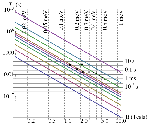
Some spin relaxation experiments have been performed on electrons in silicon dot devices (see Figure 5). Our theory for spin relaxation in the electric-dipole approximation should be valid only well before any degeneracy between Zeeman and orbital splitting is reached, the regime of a silicon spin qubit. In Ref Hayes et al. , was measured in a lateral, depletion mode Si/SiGe quantum dot for three different magnetic fields between 1 and 2 T. Comparing to Eq. 12, the data appears to follow a rate but with relatively few points it is difficult to make firm conclusions. These data points fall on the meV orbital splitting line (obtained using the value of SOC from Ref. Wilamowski et al. (2002)), which is roughly consistent with the lithographic size of the dot but differs from the meV value used for the theory model in that paper (though it is unclear if the experimental orbital splitting was measured) Hayes et al. . has also been measured in a metal-oxide-semiconductor system with the dot near the Si/SiO2 interface Xiao et al. (2010); they report measuring an orbital splitting in this device of roughly 0.4 meV. There are five data points that fit a law reasonably well; however, this behavior is observed only for T. Here theory predicts a roughly order of magnitude shorter spin relaxation time for a dot with meV (the data 3 T behave as if the orbital splitting is 1 meV). For T, is roughly independent of , with ms (possibly limited by charge noise or some other mechanism). Finally, a recent measurement of in a laterally gated Si/SiGe dot in a doped device yielded s at a field of None of the data shows evidence of hot spot (fast spin relaxation cusp) behavior.
On the whole, these experiments give good evidence that the SOC-mediated spin-phonon interaction is the dominant channel at high fields: both the B dependance and, importantly, the overall magnitude are consistent with theory. The value of the Rashba coefficient that is used in Figure 5 may not be appropriate for a MOS structure (although inversion layer spin relaxation measurements show relaxation times Shankar et al. (2010) within an order of magnitude of those found in SiGe QWs) and can vary from device to device based on material, interface roughness, electric field at the interface, etc. Nestoklon et al. (2006b); Prada et al. (2011). A much smaller SOC constant might explain the order of magnitude difference between theory and experiment for the various systems. It would be very useful in the future to attempt to characterize the SOC strength in these wafers by other means, for example via 2DEG spin relaxation Glazov (2004), although the SOC may vary at a microscopic level. It is also very important to check the dependance of on field direction. This has not yet been done experimentally. Looking beyond the electric-dipole approximation, there may be a strong and sudden increase in the relaxation rate for spin relaxation when the spin splitting matches the orbital splitting; no such effect is expected if the 1st excited state is a (pure) valley state. A complication to this picture may be a lack of mixing with the orbital state if the SOC is only Dresselhaus-like Bulaev and Loss (2005) (even in the ideal case). Lastly, our assumption of Fock-Darwin wave functions may not be correct (do to dot asymmetry, interface roughness, etc.); leading to matrix elements between dot states that influence the relaxation rate up or down.
While these results are encouraging, they do not constitute a complete vindication of theory. Hence we discuss how to combine the results of different measurements to fix some universal quantities. Specializing Eq. 6 to the first excited state, neglecting anisotropy and the dipole moment in the -direction, noting that using Eq. 7, and taking we find an orbital relaxation rate from the first excited state to the ground state:
| (18) |
With similar assumptions for the spin relaxation and specializing to an in-plane field, we have from Eq. 12
| (19) |
We wish to eliminate the poorly determined quantities and both related to the size of the dot, and the electron-phonon coupling strength and phonon velocity, in favor of measurable numbers (as far as possible). To do so, we use Eqs. 8, and 13:
| (20) |
Here is the Zeeman splitting. is the energy of the first excited state, which can be measured independently, by transport spectroscopy or looking at Orbach processes at higher temperatures. can also be measured by other means, though this is not straightforward Studer et al. (2009). Thus it would take a combination of measurements to use the absolute magnitude of as a test of theory. Note that this analysis assumes that the first excited state is purely orbital in nature and that the fast orbital relaxation time can be measured. The former may be ameliorated in the valley case where there is strong valley-orbital mixing, or if not, can be replaced with the ideal valley relaxation time. The latter may be a difficult experimental constraint. Failing this, the and the field anisotropy given by Eq. 12 provide the best tests. We note also that the field anisotropy of the spin relaxation, Eq. 12, can help determine the relative contributions of the Rashba and Dresselhaus-like SOC contributions.
We have focused on the lowest lying state configurations of a silicon quantum dot that are most relevant for quantum computing and have found that, in general, spin-based quantum computing benefits from orbital and valley states being as high in energy as possible. We began by considering phonon relaxation of excited orbital states across the same valley state in a lateral silicon QD. We found that orbital relaxation could be dramatically faster in biaxially strained silicon than in the bulk. This, for example, speeds up spin qubit initialization via optical pumping schemes Friesen et al. (2004) as well as possible leakage to excited states via phonon excitation. The phonon bottleneck effect will eventually decrease the orbital relaxation rate but only for unrealistically small dots. In contrast, spin relaxation can easily be seconds (even when the magnetic field points along the growth direction) and increases for small dots and low magnetic fields. At small magnetic fields, charge noise could play a dominant role. Valley relaxation can also be long in ideal dots, especially for small valley splittings. In non-ideal dots, although not quantitatively considered here, valley relaxation will likely be comparable to orbital relaxation.
The theory proposed here depends on the correct identification of excited states as either orbital excited states or valley excited states. Theoretical considerations for spin and valley relaxation in cases where the states are not purely orbital, valley, or spin—in other words they are mixed due to, for example, disorder or surface roughness in realistic devices—and for regimes beyond small B-field (where degeneracies come into play) are subjects for future work.
Acknowledgements.
We are grateful for helpful conversations with M. Friesen, S. N. Coppersmith, M.A. Eriksson, and R. Ruskov. We thank the group of H.W. Jiang for access to their data. RJ was supported by ARO grant no. W911NF-11-1-0030.IX Appendix
IX.1 Orbital relaxation: beyond the electric dipole approximation
To calculate the matrix element of between orbital states and in Eq. 5 beyond the electric dipole approximation, we begin with the full expression (see Eq. 4):
| (21) |
We proceed following the derivation by Castner Castner (1967). This derivation will be useful when valley relaxation is considered. A function which is periodic with the period of the lattice may be expanded in a Fourier series in the reciprocal lattice vectors , so
and the integral in becomes
The envelope probability can be Fourier transformed,
Plugging this into the integral in gives
which equals
Finally, the matrix element is given by
| (22) |
We are calculating an intra-valley scattering process (orbital relaxation with no change in valley state) so is the dominant term, , and which gives
and for the most relevant transition,
where for longitudinal phonons but for transverse phonons (). is the first coefficient in the Bloch wave expansion (see Table X for the largest contributions).
The envelope function of the ground state QD wave function in the absence of a magnetic field in the lowest approximation is a product of Gaussians, where and The excited state, if , is where
Then, the overlap integral is given by
Inserting these into the Golden Rule, we find that
| (23) | ||||
| (24) |
continuing,
We are left with calculating the three angular integrals which have units kg2/s2 and are defined as
We can immediately point out that because . Then,
If we assume an approximately circular dot in and , then using we can do the integral easily,
where
Finally, the orbital relaxation rate for a parabolic dot (in all three dimensions) from its first excited state is given by (with , the common notation)
| (25) | ||||
| (26) |
This reduces exactly to the expression for orbital relaxation within the electric dipole approximation, given in Eq. 6, when .
IX.2 Valley relaxation (ideal case)
IX.2.1 Valley relaxation in a three-dimensional parabolic quantum dot
We consider valley relaxation in a lateral silicon quantum dot. We begin where we left off in our exact consideration of orbital relaxation. Our expression for the electron-phonon matrix element, Equation 22, was
where is the Fourier transform of the envelope function overlap integral. Since the valley transition involves a change in crystal momentum, there are no intravalley terms from this expression and we must consider high wavenumber phonons that can connect the two valleys which are separated in the first Brillouin zone by . In this case, and and the matrix element becomes
where for longitudinal phonons but zero for transverse phonons (). The matrix element will only be large for values of . The shortest wavenumber phonon to connect the two valleys is the Umklapp phonon across the Brillouin zone where , where . Thus, for the and valleys,
| (27) |
This is just the result of Castner as a component of his calculation of Raman spin transitions in donors. The major difference between the donor and QD calculations (in the ideal case) are due to the different envelope functions (impurity vs. parabolic). We next require the Fourier transform of the QD envelope function:
Again we have considered the case where the dimension of the wave function can be approximated as a simple Gaussian (which is for our consideration a good approximation).
Looking at Eq. 27, we see that the -functions are heavily peaked at ( m-1) in the direction and at in the and directions. Since phonons of this magnitude are needed to connect the two valleys, resonant phonons close to this will increase the matrix element leading to increased relaxation. However, slightly off-resonant phonons can also cause a transition due to the widths of the -functions which broaden as gets smaller (see Figure 9). In donors, the valley splitting tends to be around 11 meV, not far off of this wave vector. In silicon quantum dots, the theoretically predicted values of the valley splitting range from 0 to 3 meV depending on the extent of the wave function.
To calculate the valley transition rate we employ the Golden Rule,
| (28) | ||||
| (29) |
where we have summed over phonons and the emitted phonon has wave number . At cryogenic temperature there are absolutely no large wave number phonons, so we need only consider spontaneous emission. Incorporating our expression for the matrix element, we find (with ) that
Taking the delta function, the rate becomes
where . We are again left with calculating three angular integrals which have units (kg2/s2) and are defined as
. If we assume that the dot is circular, then the -functions simplify,
Replacing with its components we can further simplify :
where
So, taking the trivial integral (no depends on ),
Now, we explicitly consider the integrals for and . Evaluating the longitudinal and transverse () integrals separately:
and, similarly,
The integrals have no analytical solution so we define a numerically tractable integral function
where
and rewrite our solutions:
and
Finally, the valley relaxation rate of a parabolic, circular quantum dot in a [001]-strained silicon quantum well is ( and )
References
- Friesen et al. (2003) M. Friesen, P. Rugheimer, D. E. Savage, M. G. Lagally, D. W. van der Weide, R. Joynt, and M. A. Eriksson, Phys. Rev. B 67, 121301 (2003).
- Loss and DiVincenzo (1998) D. Loss and D. P. DiVincenzo, Phys. Rev. A 57, 120 (1998).
- Tahan (2005) C. Tahan, Silicon in the quantum limit: Quantum computing and decoherence in silicon architectures, Ph.D. thesis, University of Wisconsin-Madison, arxiv.org/abs/0710.4263 (2005).
- Smelyanskiy et al. (2003) V. N. Smelyanskiy, A. G. Petukhov, and V. V. Osipov, Phys. Rev B 72, 081304 (2003).
- Shi et al. (2012) Z. Shi, C. B. Simmons, J. R. Prance, J. K. Gamble, T. S. Koh, Y.-P. Shim, X. Hu, D. E. Savage, M. G. Lagally, M. A. Eriksson, M. Friesen, and S. N. Coppersmith, Phys. Rev. Lett. 108, 140503 (2012).
- Feher and Gere (1959) G. Feher and E. Gere, Phys. Rev. 114, 1245 (1959).
- Pines et al. (1957) D. Pines, J. Bardeen, and C. P. Slichter, Phys. Rev. 106, 489 (1957).
- Abrahams (1957) E. Abrahams, Phys. Rev. 107, 491 (1957).
- Roth (1960) L. Roth, Phys. Rev. 118, 1534 (1960).
- (10) L. Roth, in Proc. Conf. Semicond. Physics / Lincoln Labs technical report.
- Hasegawa (1960) H. Hasegawa, Phys. Rev. 118, 1523 (1960).
- Wilson and Feher (1961) D. K. Wilson and G. Feher, Phys. Rev. 124, 1068 (1961).
- Castner (1963) T. G. Castner, Phys. Rev. 130, 58 (1963).
- Castner (1967) T. G. Castner, Phys. Rev. 155, 816 (1967).
- Kane (1998) B. E. Kane, Nature 393, 133 (1998).
- Tahan et al. (2002) C. Tahan, M. Friesen, and R. Joynt, Phys. Rev. B 66, 035314 (2002).
- Glavin and Kim (2003) B. A. Glavin and K. W. Kim, Phys. Rev. B 68, 045308 (2003).
- Khaetskii and Nazarov (2000) A. V. Khaetskii and Y. V. Nazarov, Phys. Rev. B 61, 12639 (2000).
- Khaetskii and Nazarov (2001) A. V. Khaetskii and Y. V. Nazarov, Phys. Rev. B 64, 125316 (2001).
- Glazov (2004) M. M. Glazov, Phys. Rev. B 70, 195314 (2004).
- Tahan and Joynt (2005) C. Tahan and R. Joynt, Phys. Rev. B 71, 075315 (2005).
- Zakharchenya (1984) B. P. Zakharchenya, Modern Problems in CM Sciences V.8: Optical Orientation (North-Holland, 1984).
- Tyryshkin et al. (2005) A. M. Tyryshkin, S. A. Lyon, W. Jantsch, and F. Schaffler, Phys. Rev. Lett. 94, 126802 (2005).
- Nestoklon et al. (2006a) M. O. Nestoklon, L. E. Golub, and E. L. Ivchenko, Phys. Rev. B 73, 235334 (2006a).
- Nestoklon et al. (2008) M. O. Nestoklon, E. L. Ivchenko, J.-M. Jancu, and P. Voisin, Phys. Rev. B 77, 155328 (2008).
- Prada et al. (2011) M. Prada, G. Klimeck, and R. Joynt, New Journal of Physics 13, 013009 (2011).
- Friesen et al. (2004) M. Friesen, C. Tahan, R. Joynt, and M. A. Eriksson, Phys. Rev. Lett. 92, 037901 (2004).
- Tahan (2004) C. Tahan (APS March Meeting, March 2004).
- Tahan (2003) C. Tahan (Solid State Quantum Information Processing Conference, Amsterdam, December 15-18, 2003).
- Soykal et al. (2012) O. O. Soykal, R. Ruskov, and C. Tahan, Phys. Rev. Lett. 107, 235502 (2012).
- Friesen and Coppersmith (2010) M. Friesen and S. N. Coppersmith, Phys. Rev. B 81, 115324 (2010).
- Ando et al. (1982) T. Ando, A. B. Fowler, and F. Stern, Rev. Mod. Phys. 54, 437 (1982).
- Friesen et al. (2007) M. Friesen, S. Chutia, C. Tahan, and S. N. Coppersmith, Phys. Rev. B 75, 115318 (2007).
- Schaffler (1997) F. Schaffler, Semicond. Sci. Technol. 124, 1515 (1997).
- Yu and Cardona (2001) P. Y. Yu and M. Cardona, Fundamentals of Semiconductors: Physics and Materials Properties (Springer, 2001).
- Boykin et al. (2004) T. B. Boykin, G. Klimeck, M. Eriksson, M. Friesen, S. N. Coppersmith, P. von Allmen, F. Oyafuso, and S. Lee, Appl. Phys. Lett. 84, 115 (2004).
- Ridley (1999) B. K. Ridley, Quantum Processes in Semiconductors (Oxford Press, New York, 1999).
- Herring and Vogt (1956) C. Herring and E. Vogt, Phys. Rev. 101, 944 (1956).
- Feher (1959) G. Feher, Phys. Rev. 114, 1219 (1959).
- Hanson et al. (2007) R. Hanson, L. P. Kouwenhoven, J. R. Petta, S. Tarucha, and L. M. K. Vandersypen, Rev. Mod. Phys. 79, 1217 (2007).
- Benisty (1995) H. Benisty, Phys. Rev. B 51, 13281 (1995).
- Benisty et al. (1991) H. Benisty, C. M. Sotomayor-Torres, and C. Weisbuch, Phys. Rev. B 44, 10945 (1991).
- Fujisawa et al. (2002) T. Fujisawa, D. G. Austing, Y. Tokura, Y. Hirayama, and S. Terucha, Nature 419, 278 (2002).
- Greenland et al. (2010) P. T. Greenland, S. A. Lynch, A. F. G. van der Meer, B. N. Murdin, C. R. Pidgeon, B. Redlich, N. Q. Vinh, and G. Aeppli, Nature (London) 465 (2010).
- Winkler (2003) R. Winkler, Spin-Orbit Coupling Effects in Two-Dimensional Electron and Hole Systems (Springer-Verlag, 2003).
- Wilamowski et al. (2002) Z. Wilamowski, W. Jantsch, H. Malissa, and U. Rossler, Phys. Rev. B 66, 195315 (2002).
- (47) R. R. Hayes, A. A. Kiselev, M. G. Borselli, S. S. Bui, E. T. C. III, P. W. Deelman, B. M. Maune, J.-S. M. Ivan Milosavljevic, R. S. Ross, A. E. Schmitz, M. F. Gyure, and A. T. Hunter, “Lifetime measurements (t1) of electron spins in si/sige quantum dots,” ArXiv:0908.0173.
- Xiao et al. (2010) M. Xiao, M. G. House, and H. W. Jiang, Phys. Rev. Lett. 104 (2010).
- Simmons et al. (2011) C. B. Simmons, J. R. Prance, B. J. V. Bael, T. S. Koh, Z. Shi, D. E. Savage, M. G. Lagally, R. Joynt, M. Friesen, S. N. Coppersmith, and M. A. Eriksson, Phys. Rev. Lett. 106, 156804 (2011).
- L. Jacak (1998) A. W. L. Jacak, P. Hawrylak, Quantum Dots (Springer, Berlin, 1998).
- Nestoklon et al. (2006b) M. Nestoklon, L. Golub, and E. Ivchenko, Phys. Rev. B 73, 235334 (2006b).
- Bulaev and Loss (2005) D. V. Bulaev and D. Loss, Phys. Rev. B 71, 205324 (2005).
- Raith et al. (2012) M. Raith, P. Stano, F. Baruffa, and J. Fabian, Phys. Rev. B 108, 246602 (2012).
- Langsjoen et al. (2012) L. S. Langsjoen, A. Poudel, M. G. Vavilov, and R. Joynt, Phys. Rev. A (2012).
- de Sousa (2003) R. de Sousa, Spin relaxation and manipulation of localized states in semiconductors: Considerations for solid state quantum computer architectures, Ph.D. thesis, University of Maryland-College Park (2003).
- Tyryshkin et al. (2003) A. M. Tyryshkin, S. A. Lyon, A. V. Astashkin, and A. M. Raitsimring, Phys. Rev. B 68, 193207 (2003).
- Saraiva et al. (2011) A. L. Saraiva, M. J. Calderon, R. B. Capaz, X. Hu, S. D. Sarma, and B. Koiller, Phys. Rev. B 84, 155320 (2011).
- Shankar et al. (2010) S. Shankar, A. M. Tyryshkin, J. He, and S. A. Lyon, Phys. Rev. B 82, 195323 (2010).
- Studer et al. (2009) M. Studer, S. Schon, K. Ensslin, and G. Saliz, Phys. Rev. B 79, 045302 (2009).