Amplification of the photocurrent in SiO2(Co)/GaAs heterostructure induced by magnetic field in the avalanche regime
Abstract
Amplification of the photocurrent in heterostructures of silicon dioxide films containing cobalt nanoparticles grown on gallium arsenide SiO2(Co)/GaAs has been observed in magnetic field in the avalanche regime. While the avalanche process is suppressed by the magnetic field and the current decreases, for photon energy greater than the GaAs bandgap energy the photocurrent significantly increases. The amplification reaches 9.5 for eV. The effect of the photocurrent amplification is explained by the spin-dependent recombination process at deep impurity centers in GaAs.
pacs:
72.40.+w, 75.47.-mThe explosive growth of the quantum-information science involving encoding, communication, manipulation, and measurement of information using quantum-mechanical objects leads to the intensive research of single-photon avalanche diodes (SPADs) Hadf09 ; Eisa11 ; Fish12 . In addition to the quantum-information science, SPADs are used in bioluminescence detection, DNA sequencing, light ranging, picosecond imaging, single-molecule spectroscopy, diffuse optical tomography, etc Iso95 ; Rech04 ; Pell00 ; Stell04 ; Mich07 ; Piff08 . SPADs have high detection efficiencies, high sensitivities, low dark count rates, and low jitter times Hadf09 ; Eisa11 . But, with the above-mentioned advantages, these devices possess the deficiency – high recovery times, during which detectors are unable to register photons. High recovery times lead to limitation the ability to resolve photon number. This problem can be resolved, if incident photons not only create photo-induced carriers, but influence on the avalanche feedback during the recovery time. In this case, one can evaluate number of photons by means of a current change flowing through an avalanche detector.
The action of incident photons on the avalanche feedback can be realized in metal-dielectric heterostructures composed of thin film of amorphous silicon dioxide with cobalt nanoparticles deposited on -type gallium arsenide substrates SiO2(Co)/GaAs. The avalanche process in SiO2(Co)/GaAs heterostructures is initiated by electrons injected from the SiO2(Co) film Lut09 . The avalanche positive feedback is caused by holes generated by the impact ionization and moved to the potential barrier nearby the interface Lut06a . Due to the positive feedback, the extremely large magnetoresistance and the negative photoconductance have been observed Lut09 ; Lut05 ; Lut12 .
In order to reach action of light on the avalanche positive feedback and, therefore, to get high changes of the photocurrent during the recovery process, which is equal to nanoseconds, the lifetime of photo-induced holes acted on the avalanche feedback must equal or greater than the recovery time. In this connection, it is need to note that the recombination of the charge carriers in GaAs is related mainly to nonradiative electron transitions through the localized electron levels in the forbidden energy band Mill80 ; Pag84 ; Bar96 ; Kal2005 ; Grange07 ; Ivch2010 . The rate of electron-hole recombination is determined by the spin-dependent recombination (SDR) through the localized electron levels in the semiconductor and depends on the spin states of both paramagnetic centers and free carriers. The recombination rate can be changed by an applied magnetic field. In a magnetic field electron-hole recombination is suppressed and additional free electrons and holes appear in the conduction band and in the valence band, respectively. As a result, photo-induced holes are accumulated in the barrier and the avalanche feedback can be manipulated by the light. The effect is accompanied by an amplification of the photocurrent.
In this paper, we study the expected amplification of the photocurrent in SiO2(Co)/GaAs heterostructures in the avalanche regime. The amplification is observed in magnetic field for light with the photon energy greater than the energy of the GaAs bandgap. For studied heterostructures the photocurrent amplification reaches 9.5 for eV at the applied magnetic field kOe.
Experiments were performed on heterostructures (SiO2)100-xCox/GaAs [the abridge notation is SiO2(Co)/GaAs]. -GaAs substrates with the thickness of 0.4 mm were of the (001)-orientation type. Electrical resistivity of GaAs chips was equal to 1.0 cm. Prior to the deposition process, substrates were polished by a low-energy oxygen ion beam Stog02 . The SiO2(Co) films with the thickness of 40 nm were prepared by the ion-beam deposition technique using a composite cobalt-quartz target onto GaAs substrates heated to 200∘C. The Co concentration in SiO2 matrix was specified by a relation of cobalt and quartz surface areas. The film composition was determined by the nuclear physical methods of element analysis based on spectra of the Rutherford backscattering for deuterons and nuclear reactions with deuterons. The average size of Co particles was determined by the small-angle X-ray scattering and increased with the growth of the concentration : from 3.0 nm at = 45 at.% to 4.0 nm at = 71 at.%. A protective Au layer of the thickness of 3-5 nm has been sputtered on SiO2(Co) films. The Au layer formed one ohmic contact in experiments, while the second contact was on the GaAs substrate. Since the Co-concentration is in the range 45 - 71 at.% and enables the percolation threshold, therefore, the film resistivity of 2.0-1.0 cm is much smaller than the resistivity of the GaAs. In this case, the applied voltage primarily falls on the GaAs substrates.
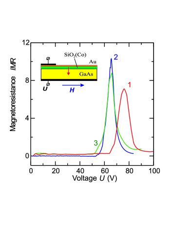
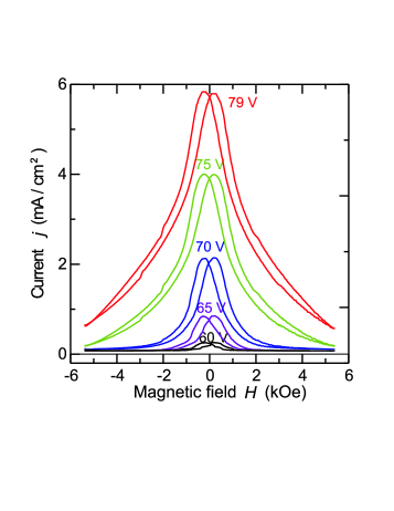
Since, the studying action of light on the avalanche is caused by the SDR and depends on a magnetic field, we choose samples with the highest influence of magnetic field on the current flowing in SiO2(Co)/GaAs heterostructures in the avalanche regime and, therefore, with the highest magnetoresistance coefficient. Magnetoresistance and influence of the magnetic field on the current at room temperature are presented in Fig. 1 and Fig. 2. Electrons are injected from the granular film into the GaAs. Figure 1 illustrates the magnetoresistance effect as a function of applied voltage. The injection magnetoresistance coefficient IMR is defined as the ratio Lut09 ; Lut05
where and are the resistances of the SiO2(Co)/GaAs heterostructure without a field and in the magnetic field , respectively; and are the current densities flowing in the heterostructure in the absence of a magnetic field and in the field . The magnetic field is equal to 2.1 kOe and is parallel to the film surface. For 52 V, a sharp increase in the current due to the process of impact ionization is observed. The applied magnetic field suppresses the avalanche process and the current flowing in the SiO2(Co)/GaAs heterostructure decreases (Fig. 2). The suppression of the avalanche process causes to the sharp growth of the IMR coefficient. As we can see from Fig. 2 the influence of the magnetic field on the current is characterized by the hysteresis loop structure.
Magnetic characterization of SiO2(Co)/GaAs heterostructures in magnetic field was done by means of the longitudinal magneto-optical Kerr effect (MOKE). Figure 3 shows magnetic hysteresis loops for the SiO2(Co)/GaAs structure with 60 at.% Co measured by MOKE (a magnetic field is aligned along the sample surface and in the plane of incidence) using a He-Ne laser with a wavelength of 632.8 nm. The value of incidence angles was of 45 deg. It is need to note that the SiO2(Co) film is in the ferromagnetic state. Taking into account the magnetoresistance values and magnetic characteristics of heterostructures presented in Fig. 1-3, we chose the SiO2(Co)/GaAs heterostructure with 60 at.% Co with the highest magnetoresistance ratio IMR for study the influence of the magnetic field on the photocurrent.

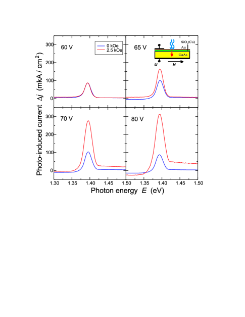
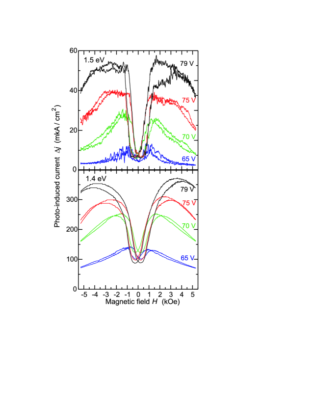
In optical experiments for measurements of the photo-induced changes of electrical current (the abridged notation is photo-induced current) in the SiO2(Co)/GaAs heterostructure, we used the lock-in technique with an intensity modulation of the light. The light beam was modulated by a chopper working at the frequency of 40 Hz and was exposed on the Au contact layer. Light penetrates through the SiO2(Co) film and reaches the GaAs substrate. The light intensity is equal to 1.0 mW/cm2. Spectral dependencies of the photo-induced current caused by the linear-polarized light at different voltages without a magnetic field and in the field 2.5 kOe are presented in Figure 4. At photon energies 1.36 eV and at voltages 65 V, in the presence of the magnetic field the photocurrent increases. If the photon energy 1.36 eV, at high voltages the negative photoconductance is observed Lut12 . Figure 5 shows the photo-induced current caused by the light radiation with photon energies 1.50 eV and 1.40 eV versus the magnetic field at different applied voltages at room temperature. In the range [-1, 1 kOe] the current is closed to the square-law dependence on the field . The photo-induced current reaches higher values at high voltages applied to the SiO2(Co)/GaAs heterostructure. For the studied heterostructure SiO2(Co)/GaAs with 60 at.% Co the photocurrent amplification is 9.5 for the photon energy eV at 79 V at the applied magnetic field kOe. The subsequent magnetic field growth leads to the avalanche suppression and to a photocurrent decrease.
To explain experimental dependencies, we consider electron-hole processes in SiO2(Co)/GaAs heterostructures in the avalanche regime. The schematic band diagram of the GaAs in the SiO2(Co)/GaAs heterostructure at the applied electrical field in the avalanche regime is shown in Fig. 6a. The semiconductor-film interface forms a potential barrier, as a consequence, electrons are accumulated between the semiconductor-film interface and the potential maximum of barrier Lut09 ; Lut06a . Without a light radiation, the injected electrons excite the process of impact ionization producing holes in the valence band. The holes move toward the barrier and are accumulated there. This lowers the potential maximum of barrier and increases the electron current leading to an enhancement of the avalanche. Due to the formed positive feedback, a small variation of the potential maximum leads to strong changes in the electron current.
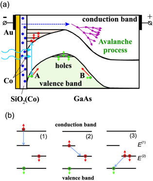
The interface region of the GaAs contains oxygen ions leaved after the polished process. According to Refs. Lin76 ; Yu84 in addition to the EL2 defect level there are oxygen-ion levels in the GaAs bandgap with energies eV, eV, eV, and eV counted from the bottom of the conduction band. At room temperature levels with energies , and are occupied by electrons. Conductivity in the conduction band is determined by thermally activated electrons from the level eV. These localized levels are of great importance for the SDR – conduction electrons and holes created in excess recombine through intermediate recombination center.
Let us consider the photocurrent amplification for the light with the photon energy , where is the bandgap energy. The light with the photon energy is absorbed in the semiconductor region near the interface and creates electrons in the conduction band and holes in the valence band in the interface region. According to theoretical models of the SDR developed in Bar96 ; Ivch2010 ; Lep72 ; White77 ; Kapl78 ; Vlas95 ; Bohme2002 , the recombination event is preceded by the trapping of conduction electrons to localized electron levels (Fig. 6b). In order to find photocurrent dependencies on the magnetic field, we consider two electrons on a pair of localized levels with different energies and . The spin conservation law permits an electron transition from the first level to the second level and a further recombination occurs if the electron pair on the levels and is in the single state . By contrast, the transition is prohibited, when the triplet states , and of the pair appears. In this case, a further recombination is highly suppressed. Under the assumption that triplet states cannot recombine and singlet states recombines with a probability , the average recombination probability of electrons on levels and is written as .
In the presence of the external magnetic field levels and are splitted. Neumann’s density operator of electrons on splitted levels in a thermal equilibrium is represented in the Boltzmann form Bohme2002
where is the temperature, , , , , are Zeeman energies of singlet and triplet states, respectively, is the -factor of electrons on localized states, is the Bohr magneton. We consider a change of the average recombination probability of electrons on a highly saturated non-equilibrium state with the density operator
Then, the change of the average recombination is
| (1) |
Taking into account that the photoconductivity and the number of photo-induced electrons in the conduction band and the number of holes in the valence band are inversely proportional to the recombination probability and , in the second order of the Taylor-series expansion of the relation (1) we find
| (2) |
Additional holes move toward the barrier and are accumulated in the barrier region (Fig. 6a). The barrier height lowers. This leads to the observed increase of the electron current and to the enhancement of the avalanche in the applied magnetic field. Such positive feedback produced by photo-induced holes and additional photo-induced electrons result in strong changes in the electron current . The experimentally observed quadratic dependence of the photocurrent from the magnetic field at low field values (Fig. 4) corresponds to the relation (2) and confirms the magnetic dependence obtained in theoretical models developed in Lep72 ; White77 . At high values of the magnetic field , the avalanche is suppressed and the photocurrent decreases.
In summary, we observe significant influence of magnetic field on photocurrent flowing in SiO2(Co)/GaAs heterostructures in the avalanche regime. While the avalanche process is suppressed by the magnetic field and the current decreases, for photon energy greater than the GaAs bandgap energy the photocurrent significantly increases. The amplification reaches 9.5 for eV at the applied magnetic field kOe. The photocurrent amplification is explained by the spin-dependent recombination through the localized electron levels in the semiconductor. In a magnetic field electron-hole recombination is suppressed. This leads to additional free electrons in the conduction band and holes in the valence band. As a result, photo-induced holes are accumulated in the barrier, the photocurrent grows and the avalanche feedback can be manipulated by the light. The photocurrent amplification effect can be used in single-photon avalanche diodes to register photons during recovery times and to resolve photon number.
The authors gratefully acknowledge the assistance of V.M. Lebedev (PNPI, Gatchina, Leningrad region, Russia) for determination of the film composition. This work was supported by the Russian Foundation for Basic Research (Project Nos. 10-02-01008, 10-02-00516, 10-02-90023).
e-mail: l_lutsev@mail.ru
References
- (1) R.H. Hadfield, Nature Photonics 3, 696 (2009).
- (2) M.D. Eisaman, J. Fan, A. Migdall, and S. V. Polyakov, Rev. Sci. Instrum. 82, 071101 (2011).
- (3) M.W. Fishburn, Fundamentals of CMOS Single-Photon Avalanche Diodes (Delft, Delft University of Technology, 2012).
- (4) T. Isoshima, Y. Isojima, K. Hakomori, K. Kikuchi, K. Nagai, and H. Nakagawa, Rev. Sci. Instrum. 66, 2922 (1995).
- (5) I. Rech, A. Restelli, S.Cova, M. Ghioni, M. Chiari, and M. Cretich, Sensors and Actuators B 100, 158 (2004).
- (6) S. Pellegrini, G.S. Buller, J.M. Smith, A.M. Wallace, and S. Cova, Meas. Sci. Technol. 11, 712 (2000).
- (7) F. Stellari, A. Tosi, F. Zappa, ans S. Cova, IEEE Trans. Instrum. Meas. 53, 163 (2004).
- (8) X. Michalet, O.H.W. Siegmund, J.V. Vallerga, P. Jelinsky, J.E. Millaud, and S. Weiss, J. Mod. Opt. 54, 239 (2007).
- (9) A. Pifferi, A. Torricelli, L. Spinelli, D. Contini, R. Cubeddu, F. Martelli, G. Zaccanti, A. Tosi, A. D. Mora, F. Zappa, and S. Cova, Phys. Rev. Lett. 100, 138101 (2008).
- (10) L. V. Lutsev, A. I. Stognij, and N. N. Novitskii, Phys. Rev. B80, 184423 (2009).
- (11) L. V. Lutsev, J. Phys.: Condensed Matter 18, 5881 (2006).
- (12) L.V. Lutsev, A.I. Stognij, and N.N. Novitskii, JETP Lett. 81, 514 (2005).
- (13) L.V. Lutsev, V.V. Pavlov, P.A. Usachev, A.A. Astretsov, A.I. Stognij, and N.N. Novitskii, Appl. Phys. Lett. 101, 242104 (2012).
- (14) R C. Miller, W.T. Tsang, and W.A. Nordland, Jr., Phys. Rev. B 21, 1569 (1980).
- (15) D. Paget, Phys. Rev. B 30, 931 (1984).
- (16) A. V. Barabanov, O. V. Tretiak, and V. A. L vov, Phys. Rev. B 54, 2571 (1996).
- (17) V.K. Kalevich, E.L. Ivchenko, M.M. Afanasiev, A.Yu. Shiryaev, A.Yu. Egorov, V.M. Ustinov, B. Pal, and Y. Masumoto, JETP Letters, 82, 455 (2005).
- (18) T. Grange, E.A. Zibik, R. Ferreira, G. Bastard, B.A. Carpenter, P.J. Phillips, D. Stehr, S. Winnerl, M. Helm, M.J. Steer, M. Hopkinson, J.W. Cockburn, M.S. Skolnick, and L.R. Wilson, New J. Phys. 9, 259 (2007).
- (19) E.L. Ivchenko, V.K. Kalevich, A.Yu. Shiryaev, M.M. Afanasiev, and Y. Masumoto, J. Phys.: Condens. Matter 22, 465804 (2010).
- (20) A.I. Stognij, N.N. Novitskii, and O.M. Stukalov, Tech. Phys. Lett. 28, 17 (2002).
- (21) A.L. Lin, E. Omelianovski, and R.H. Bube, J. Appl. Phys. 47, 1852 (1976).
- (22) P.W. Yu, Appl. Phys. Lett. 44, 330 (1984).
- (23) D.J. Lepine, Phys. Rev. B 6, 436 (1972).
- (24) R. M. White and J. F. Gouyet, Phys. Rev. B 16, 3596 (1977).
- (25) D. Kaplan, I. Solomon, and N. F. Mott, J. Phys. (Paris) Lettres 39, L51 (1978).
- (26) L.S. Vlasenko, Yu.V. Martynov, T. Gregorkiewicz, and C.A.J. Ammerlaan, Phys. Rev. B 52, 1144 (1995).
- (27) C. Böhme, Ph.D. Thesis, Philipps Universität Marburg/ Lahn, 2002.