Tunneling properties of vertical heterostructures of multilayer hexagonal boron nitride and graphene
Abstract
We use first-principle density functional theory (DFT) to study the transport properties of single and double barrier heterostructures realized by stacking multilayer h-BN or BC2N, and graphene films between graphite leads. The heterostructures are lattice matched. The considered single barrier systems consist of layers of up to five h-BN or BC2N monoatomic layers (Bernal stacking) between graphite electrodes. The transmission probability of an h-BN barrier exhibits two unusual behaviors: it is very low also in a classically allowed energy region, due to a crystal momentum mismatch between states in graphite and in the dielectric layer, and it is only weakly dependent on energy in the h-BN gap, because the imaginary part of the crystal momentum of h-BN is almost independent of energy. The double barrier structures consist of h-BN films separated by up to three graphene layers. We show that already five layers of h-BN strongly suppress the transmission between graphite leads, and that resonant tunneling cannot be observed because the energy dispersion relation cannot be decoupled in a vertical and a transversal component.
pacs:
81.05.ue,72.80.Vp,73.63.-b,73.50.-h,71.15.MbMobility of suspended graphene can be extremely high, as demonstrated by experiments and theory Bolotin et al. (2008); Du et al. (2008); Amad and Sarma (2008); Borysenko et al. (2010). However, use of graphene in solid state devices typically requires deposition or growth on a dielectric substrate, which can strongly suppress mobility, due to electron coupling with dielectric-layer phonon modes, as demonstrated in the case of SiO2 or HfO2, the most commonly used dielectric materials Morozov et al. (2008); Betti et al. (2011).
Hexagonal boron nitride (h-BN) has been recently investigated as a promising dielectric for graphene Britnell et al. (2012a); Dean et al. (2010); Ponomarenko et al. (2009); Amet et al. (2012), while boron nitride domains has been suggested as a way to engineer graphene nanoribbon transport properties Lopez-Bezanilla and Roche (2012).
h-BN has hexagonal geometry and a lattice constant closely matching that of graphene Meyer et al. (2009), and the electronic interaction of h-BN with a single graphite sheet Dean et al. (2010); Decker et al. (2011) or with bilayer graphene Ramasubramaniam et al. (2011) is very weak. As a result, graphene deposited on an h-BN substrate maintains its electronic and transport properties.
From this perspective, understanding transport along stacked graphene/h-BN structure can provide relevant information regarding the leakage current in graphene based Field Effect Transistors exploiting h-BN as gate dielectric or the performance of recently proposed vertical devices Britnell et al. (2012b); Kumar et al. (2012).
In this work, with ab-initio method, we calculate the quantum transport in single and double barriers consisting of h-BN and BCN layers between semi infinite graphite leads, using the formalism introduced by Choi et al. Choi and Ihm (1999). Barrier consists of up to five h-BN or h-BC2N atomic layers arranged as shown in Fig. 1, according to a recent paper by Ribeiro Ribeiro and Peres (2011). The double barrier is made of two or four h-BN or h-BC2N layers separated by up to three graphene layers. The scattering region considered in the calculation includes at least four atomic layers of graphite on each side of the barrier film, to ensure that the charge density does not change at the interface between the lead and the scattering region. The geometry of the total structure in the scattering zone has been optimized.
Ab-initio calculations have been performed by means of Quantum Espresso Giannozzi et al. (2009), using a plane wave basis set in the local density approximation (LDA) Perdew and Zunger (1981). A 35 Ry wave function cutoff has been considered, the Brillouin zone has been sampled using a MonkhorstPack grid. Atomic positions have been relaxed using a conjugate gradient algorithm until all components of all forces was smaller than 0.01 eV/Åwhile the electronic minimization has been performed with a tolerance of eV. It has been shown Giovannetti et al. (2007) that LDA provides a reliable description of the geometry and the electronic structure in the presence of weak interactions between h-BN layers or between h-BN and graphene layers. On the other hand, the LDA representation for the exchange-correlation potential cannot correctly describe the excited states in organic systems and leads to overestimation of conductance. However, following other works on this subject Kuroda et al. (2011), we expect that these effects have only minor consequences, and thus our conclusions should not be affected by this choice. The transmission probabilities have been calculated with the PWCOND Smogunov et al. (2004) module of Quantum Espresso. The transport properties are studied in the framework of Landauer formalism, Landauer (1970); Buttiker et al. (1985) where the ballistic conductance is given by , where is the quantum conductance , and is the total transmission at the energy .
is obtained as
| (1) |
where is the probability that an electron with energy and transversal momentum incoming from the th Bloch state is transmitted to the outgoing th state of the other electrode. Sums runs on both spins. The first sum is performed over belonging to the two-dimensional Brillouin zone (2D-BZ) of the supercell.
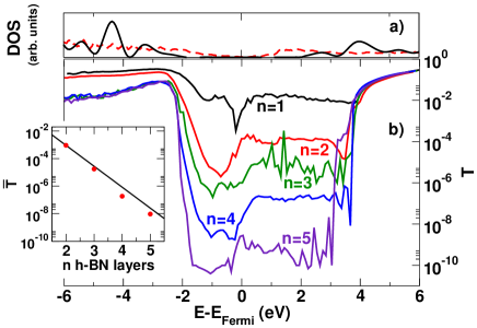
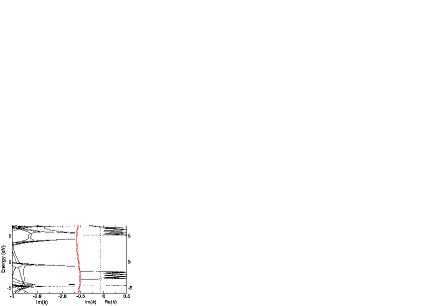
The transmission probability of a single h-BN barrier is shown in Fig. 2 for a different number of layers. For a given number of single h-BN layers, the transmission probability is almost independent of energy, in an energy range of about 3 eV starting from the Fermi level. This behavior can be explained by the structure of the complex bands in bulk h-BN shown in Fig. 3: in the energy interval considered, in the symmetry point K on the plane parallel to the layer interface (where the graphite states with real momentum reside), h-BN has a dispersion relationship according to which the imaginary wave vector is almost independent of energy, and therefore as well. Of course decays exponentially with increasing , as can be verified by plotting the average value in the energy range between the Fermi energy value and 3.4 eV above as a function of the number of layers, as in the inset of Fig. 2. The fitting exponential is
| (2) |
and five h-BN layers strongly suppress the transmission. The dip in correspondence of eV is due to the null density of states in graphite leads. In addition, we also note that for eV, the transmission probability is suppressed even in a classically allowed region, probably because of a mismatch between propagating states in the h-BN barrier and in graphite.
In Fig. 4, the transmission probability as a function of energy is shown for a single barrier of BC2N of atomic layers between graphite leads. The atomic structure is shown in the inset. A qualitatively similar behavior as h-BN is observed, with an exponential decay of the transmission probability in a narrow range around Fermi energy. BC2N has a gap of 1.6 eV.
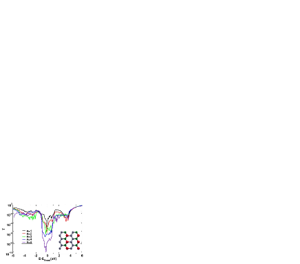
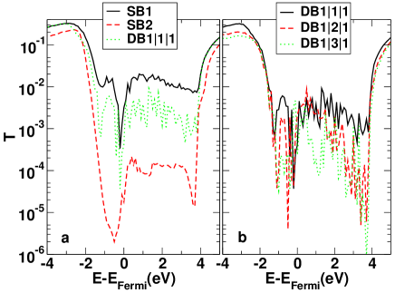
Fig. 5 shows the transmission probability as a function of energy for some single and double barrier structures. All these systems are symmetrical, with two identical barriers separated by one, two or three graphene layers. For clarity, hereinafter, we have indicated the single barrier systems with the acronym SB followed by the number of h-BN layer (e.g. in Fig. 1a, SB5). In the same way, the double barrier systems are related with DB and three numbers, namely the number of h-BN layers on the left, the number of graphene layers in the central region, and the number of h-BN layers on the right (e.g. in Fig. 1c, DB212). By comparing the transmission of the single h-BN barrier (SB1) with that of the double h-BN barrier (DB111) (Fig. 5a), the noteworthy aspect is that the insertion of a single graphene sheet has a noticeable effect on transport even in the direction perpendicular to the plane (Fig. 5). While the insertion of even a single BN (SB1) sheet strongly suppresses the transmittance (particularly in the zone near the Fermi energy), the presence of a triple layer (DB111) yields almost the same behavior as the single-BN sheet . In addition, DB111 has a much higher transmittance than SB2, despite the identical number of h-BN layers. In Fig. 5b, we report the transmittance of double-barrier systems in which two h-BN layers are separated by one, two or three graphene layers.
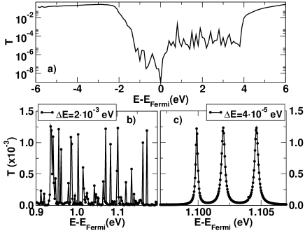
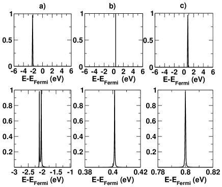
It is also important to notice that no resonant tunneling occurs in the double barrier structures, in the whole energy range explored, as we have verified with a very dense energy sampling of transmission probability, down to steps of eV, as shown in Fig. 6 referred to (DB212) case. The reason is due to the fact that the energy dispersion relation in graphene cannot be written as the sum of a longitudinal and a transversal component. Therefore, for each transversal wave vector , one observes resonances in with unity transmission probability peaks, as shown in Fig. 7, at different energies. When the sum over resonance do not occur at the same energy and are therefore washed out.
I Conclusion
In this paper we have investigated the tunneling probability of vertical heterostructures consisting of single and double layers of h-BN and BC2N separated by graphene sheets and connected to graphite leads. These structures are interesting from the point of view of graphene electronics, also because few devices have been proposed in which transport occurs in the direction perpendicular to graphene planes Britnell et al. (2012b); Yang et al. (2012); Fiori et al. . As expected, the transmission probability is exponentially dependent on the number of layers, and is already strongly suppressed by a single monolayer of h-BN or BC2N. In addition, due to the energy dispersion relationship in the energy gap, for which the imaginary wave vector is almost constant as a function of energy, the transmission probability has only small dependence on energy. We have also shown that resonant tunneling is completely suppressed by the peculiar energy dispersion relation of graphene, that cannot be decomposed in the sum of a longitudinal and a transversal component.
II Acknowledgment
This work was supported in part by the EC 7FP through the Project GRADE (Contract 317839).
References
- Bolotin et al. (2008) K. I. Bolotin, K. J. Sikes, Z. Jiang, M. Klima, G. Fudenberg, J. Hone, P. Kimi, and H. L. Stormer, Solid State Commun 146, 351 (2008).
- Du et al. (2008) X. Du, I. Skachko, A. Barker, and E. Y. Andrei, Nat. Nanotechnology 3, 491 (2008).
- Amad and Sarma (2008) S. Amad and S. D. Sarma, Solid State Commun 146, 356 (2008).
- Borysenko et al. (2010) K. Borysenko, J. T. Mullen, E. A. Barry, S. Paul, Y. G. Semenov, J. K. Zavada, M. B. Nardelli, and K. W. Kim, Phys. Rev. B 81, 121412(R) (2010).
- Morozov et al. (2008) S. V. Morozov, K. S. Novoselov, M. I. Katsnelson, F. Schedin, D. C. Elias, J. A. Jaszczak, and A. K. Geim, Phys. Rev. Lett. 100, 016602 (2008).
- Betti et al. (2011) A. Betti, G. Fiori, and G. Iannacone, App. Phys. Lett. 98, 212111 (2011).
- Britnell et al. (2012a) L. Britnell, R. V. Gorbachev, R. Jalil, B. D. Belle, F. Schedin, M. I. Katsnelson, L. Eaves, S. V. Morozov, A. S. Mayorov, N. M. R. Peres, A. H. Castro Neto, J. Leist, A. K. Geim, L. A. Ponomarenko, and K. S. Novoselov, Nano Letters 12, 1707 (2012a), http://pubs.acs.org/doi/pdf/10.1021/nl3002205 .
- Dean et al. (2010) C. R. Dean, A. F. Young, I. Meric, C. Lee, L. Wang, S. Sorgenfrei, K. Watanabe, T. Taniguchi, P. Kim, K. L. Shepard, and J. Hone, Nat. Nanotechnol 5, 722 (2010).
- Ponomarenko et al. (2009) L. A. Ponomarenko, R. Yang, T. M. Mohiuddin, M. I. Katsnelson, K. S. Novoselov, S. V. Morozov, A. A. Zhukov, F. Schedin, E. W. Hill, and A. K. Geim, Phys. Rev. Lett. 102, 206603 (2009).
- Amet et al. (2012) F. Amet, J. R. Williams, A. G. F. Garcia, M. Yankowitz, K. Watanabe, T. Taniguchi, and D. Goldhaber-Gordon, Phys. Rev. B. 85, 073405 (2012).
- Lopez-Bezanilla and Roche (2012) A. Lopez-Bezanilla and S. Roche, Phys. Rev. B 86, 165420 (2012).
- Meyer et al. (2009) J. C. Meyer, A. Chuvilin, G. Algara-Siller, J. Biskupek, and U. Kaiser, Nano Lett. 9, 2683 (2009).
- Decker et al. (2011) R. Decker, Y. Wang, V. W. Brar, W. Regan, H.-Z. T. ans Q. Wu, W. Gannett, A. Zettl, and M. F. Crommie, Nano Lett 11, 2291 (2011).
- Ramasubramaniam et al. (2011) A. Ramasubramaniam, D. Naveh, and E. Towe, Nano Lett 11, 1070 (2011).
- Britnell et al. (2012b) L. Britnell, R. V. Gorbachev, R. Jalil, B. D. Belle, F. Schedin, A. Mishchenko, T. Georgiou, M. I. Katsnelson, L. Eaves, S. V. Morozov, N. M. R. Peres, J. Leist, A. K. Geim, K. S. Novoselov, and L. A. Ponomarenko, Science 335, 947 (2012b).
- Kumar et al. (2012) S. B. Kumar, G. Seol, and J. Guo, Applied Physics Letters 101, 033503 (2012).
- Choi and Ihm (1999) H. J. Choi and J. Ihm, Phys. Rev. B 59, 2267 (1999).
- Ribeiro and Peres (2011) R. M. Ribeiro and N. M. R. Peres, Phys. Rev. B 83, 235312 (2011).
- Giannozzi et al. (2009) P. Giannozzi, S. Baroni, N. Bonini, M. Calandra, R. Car, C. Cavazzoni, D. Ceresoli, G. L. Chiarotti, M. Cococcioni, I. Dabo1, A. D. Corso, S. de Gironcoli, S. Fabris, G. Fratesi, R. Gebauer, U. Gerstmann, C. Gougoussis, A. Kokalj, M. Lazzeri, L. Martin-Samos, N. Marzari, F. Mauri, R. Mazzarello, S. Paolini, A. Pasquarello, L. Paulatto, C. Sbraccia, S. Scandolo, G. Sclauzero, A. P. Seitsonen, A. Smogunov, P. Umari1, and R. M. Wentzcovitch1i, J. Phys.: Condens. Matter 21, 395502 (2009).
- Perdew and Zunger (1981) J. P. Perdew and A. Zunger, Phys. Rev. B 23, 5048 (1981).
- Giovannetti et al. (2007) G. Giovannetti, P. A. Khomyakov, G. Brocks, P. J. Kelly, and J. van den Brink, Phys. Rev. B 76, 073103 (2007).
- Kuroda et al. (2011) M. A. Kuroda, J. Tersoff, D. M. Newns, and G. J. Martyna, Nano Letters 11, 3629 (2011).
- Smogunov et al. (2004) A. Smogunov, A. DalCorso, and E. Tosatti, Phys. Rev. B 70, 045417 (2004).
- Landauer (1970) R. Landauer, Philos Mag 21, 863 (1970).
- Buttiker et al. (1985) M. Buttiker, Y. Imry, and R. Landauer, Phys Rev B 31, 6207 (1985).
- Yang et al. (2012) H. Yang, J. Heo, S. Park, H. Song, D. Seo, K.-E. Byun, P. Kim, I. Yoo, H.-J. Chung, and K. Kim, Science 336, 1140 (2012).
- (27) G. Fiori, S. Bruzzone, and G. Iannaccone, IEEE Transactions on Electron Devices, to appear .