Quantum spin Hall effect induced by electric field in silicene
Abstract
We investigate the transport properties in a zigzag silicene nanoribbon in the presence of an external electric field. The staggered sublattice potential and two kinds of Rashba spin-orbit couplings can be induced by the external electric field due to the buckled structure of the silicene. A bulk gap is opened by the staggered potential and gapless edge states appear in the gap by tuning the two kinds of Rashba spin-orbit couplings properly. Furthermore, the gapless edge states are spin-filtered and are insensitive to the non-magnetic disorder. These results prove that the quantum spin Hall effect can be induced by an external electric field in silicene, which may have certain practical significance in applications for future spintronics device.
pacs:
73.20.At, 73.22.-f, 73.63.-bRecently, the quantum spin Hall effect (QSHE) has attracted significant interests in the fields of condensed matter physics and material science as it constitutes a new phase of matter and has potential applications in spintronics.Kane ; Bernevig ; Konig ; CXLiu ; CCLiu The novel electronic state with a nontrivial topological property and time-reversal invariance has a bulk energy gap separating the valence and conduction bands and a pair of gapless spin-filtered edge states sat the sample boundaries. The QSHE has been first predicted by Kane and Mele in graphene in which the intrinsic spin-orbit coupling opens a band gap at the Dirac points.Kane However, the QSHE can occur in graphene only at unrealistically low temperatures since the intrinsic spin-orbit coupling in graphene is rather weak.Yao ; DHH ; Min Therefore, it is crucial to search new materials with strong spin-orbit coupling for realizing the QSHE. Recent theories and experiments provide evidences of the QSHE in two-dimensional HgTe-CdTe quantum wells.Konig ; Bernevig
Very recently, a close relative of graphene, a slightly buckled honeycomb lattice of Si atoms called silicene has been synthesized.Lalmi ; Feng ; Chen ; Aufray ; Padova Silicene can be well compatible with current silicon based electronic technology. Many progresses in the study of silicene have been made, both experimentally and theoretically. For example, electronic properties and the giant magnetoresistance in silicene have been reported.Ding1 ; Houssa ; Ding2 ; Kang Moreover, almost every striking property of graphene could be transferred to silicene.Padova ; Houssa2 It has been theoretically shown that the strong intrinsic spin-orbit coupling in silicene may lead to detectable QSHE.CCLiu ; Cahangirov ; CCLiu2 ; Ezawa1 ; Ezawa2 ; An
In this paper, we provide systematic investigations on the band structures and electron transport properties of silicene in the presence of an external electric field. Silicene consists of a buckled honeycomb lattice of silicon atoms with two sublattices A and B. We take a silicene sheet on the plane, and apply the electric field in direction. The electric field generates a staggered sublattice potential between silicon atoms at A sites and B sites due to the buckled structure of the silicene. On the other hand, two kinds of Rashba spin-orbit coupling, referring to the nearest and next-nearest neighbor hoppings respectively, can also be tuned by the external electric field. We find that a gap can be opened by the staggered sublattice potential and gapless edge states are induced in the gap by Rashba spin-orbit coupling. We predict that the QSHE can be observed by applying an external electric field in silicene even if the intrinsic spin-orbit coupling in the system is very weak.
In the tight-binding representation, the silicene sample with an external electric field can be described by the the following Hamiltonian:CCLiu2
| (1) | |||||
where creates an electron with spin polarization at site ; and run over all the nearest and next-nearest neighbor hopping sites, respectively. The first term is the nearest-neighbor hopping with the transfer energy . The second term is the staggered sublattice potential term, where for the A (B) site and is the potential energy induced by the external electric field. The third and fourth terms, respectively, represent the first Rashba spin-orbit coupling associated with the nearest neighbor hopping and the second Rashba spin-orbit coupling associated with the next-nearest neighbor hopping. Both of them are induced by the external electric field. Here is the Pauli matrix of spin and with the vector connecting two sites and . The intrinsic SOC term has been ignored intentionally since the main focus of this work is the Rashba terms and the staggered potential, which can be tuned by the external electric field.
We assume that the temperature is set to zero and two semi-infinite silicene ribbons are employed as left and right leads. The two-terminal conductance of the system can be calculated by the nonequilibrium Green’s function method and Landauer-Büttiker formula as
| (2) |
where is the line-width function and is the retarded Green function with the Hamiltonian in the center region .Ren The self-energy due to the semi-infinite lead- can be calculated numerically.Sancho
With the help of the nonequilibrium Green’s function method, the local current flowing on site with spin can be expressed as
| (3) | |||||
where is the matrix element of the lesser Green s function of the scattering region and is the current from site to . After taking Fourier transformation, the local current can be calculated as
| (4) |
Eq. (4) has been widely used in the local-current studies of tight-binding models. Nikolic ; Jiang ; Xing When the sample is at zero temperature and the applied voltage is small, by applying the Keldysh equation with the Fermi distribution function , Jauho the Eq. (4) can be written as
| (5) | |||||
where and are the voltages at the Lead-L and R, respectively. is electron correlation function. The first part of Eq. (5) can only generate the equilibrium current and does not contribute to the transport, so it can be dropped out in present work. It is the second part that gives rise to the nonequilibrium current.
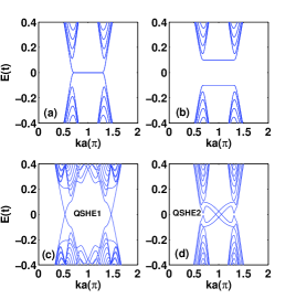
In the following numerical calculations, we use the hopping energy as the energy unit. The width of the zigzag ribbon is , where is the silicon-silicon distance. In Fig. 1 we show the energy bands obtained from diagonalizing the tight-binding Hamiltonian (1) with various parameters for a zigzag nanoribbon. The nanoribbon with only the nearest-neighbor hopping shows a semi-metallic behavior, as shown in Fig. 1 (a). An energy gap can be opened due to the inversion symmetry breaking induced by the staggered sublattice potential and the magnitude of the gap is (see Fig. 1 (b)). When the first and second Rashba spin-orbit couplings induced by the external electric field are taken into account properly, which turn silicene from normal insulating to quantum spin Hall regime, gapless edge states appear within the band gap (see Figs. 1 (c) and (d)). The gapless edge states with different spins connect the conduction band and valence band. As usual, these gapless edge states are originated from the nontrivial topological orders in the bulk. According to different values of the first Rashba spin-orbit coupling, the QSHE induced by the external electric field can be divided into two types, QSHE1 and QSHE2. In QSHE1, when the first Rashba spin-orbit coupling is strong, the edge states traverse the bulk gap within each valley, as shown in Fig. 1 (c). However, in QSHE2 when the first Rashba spin-orbit coupling is weak, the edge states inter-connect two valleys. Moreover, they bend and give rise to “subgaps” around and , which makes the structure of propagating channels complicated in the bulk gap.
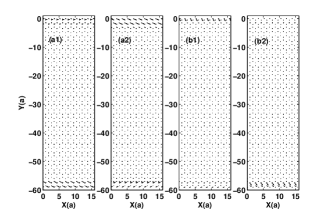
To investigate the QSHE induced by the external electric field in more details, the configurations of the spin-dependent local-current-flow vector are plotted in Fig. 2. We focus only on the left-injected current. The Fermi energy is set to be for QSHE1 (Fig. 2 (a)) and for QSHE2 (Fig. 2 (b)). For these Fermi energies, there are only the lowest transmission channels, i.e., the gapless edge states. For QSHE1, the spin-up local currents locate mainly on the lower edge (see Fig. 2 (a1))and the spin-down local currents locate mainly on the upper edge (see Fig. 2 (a2)). Contrary to QSHE1, for QSHE2, the spin-up local currents locate mainly on the upper edge (see Fig. 2 (b1)) and the spin-down local currents locate mainly on the lower edge (see Fig. 2 (b2)). These results show that the gapless edge states are spin-filtered and the two kinds of Rashba spin-orbit couplings can drive an ordinary insulating state of the silicene to the topological insulator.
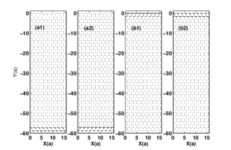
Next, for QSHE1, the Fermi energy is tuned to or , reaching slightly into the bulk band. The configurations of spin-dependent local-current-flow vector in such regions are plotted in Fig. 3. We find that the edge states are not fully spin-filtered when they are inside the bulk band. However, in this case, the electrons flow along the lower edge (see Fig. 3 (a)), while the holes flow forward along the upper edge (see Fig. 3 (b)).
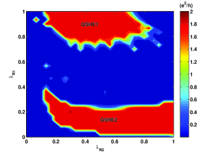
In order to have a global view on the phase transitions, the phase diagram at is plotted in Fig. 4. When these two kinds of spin-orbit couplings are tuned properly, two kinds of QSHE, QSHE1 and QSHE2 appear. For QSHE1, the silicene nanoribbon has a large bulk gap and there are only gapless edge states in the bulk gap because the first spin-orbit coupling can widen the bulk gap.Ezawa1 On the other hand, for QSHE2, the system has a narrow bulk gap and even the gapless edge states is located in the bulk band because the second spin-orbit coupling can narrow the bulk gap.Ezawa3
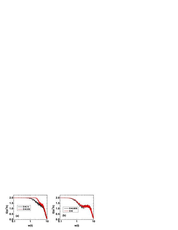
Finally, we examine the non-magnetic disorder effect on the conductance plateau of the QSHE. Random on-site potential is added for each site in the central region, where is uniformly distributed in the range with the disorder strength . Figs. 5 (a) and (b) show the conductance versus the disorder strength at various energy for QSHE1 and QSHE2, respectively. The results show that these quantum plateaus are robust against non-magnetic disorder because of the topological origin of the edge states. Especially, the quantum plateau of QSHE1 maintains its quantized value very well even when reaches for , as shown in Fig. 5 (a). We can also find that the gapless edge states of QSHE1 are more insensitive to the non-magnetic disorder than those of QSHE2 because the bulk gap of QSHE1 is larger than that of QSHE2. With further increasing of the disorder strength, the conductance gradually reduce to zero and the system eventually enters the insulating regime.
In summary, we predict that the QSHE can be induced by applying an electric field in silicene even if the intrinsic spin-orbit coupling is very weak. The energy bands, the configurations of the spin-dependent local-current-flow vector, and the conductance of the system are numerically studied using the tight-binding Hamiltonian. The first and second Rashba spin-orbit couplings, referring to the nearest and next-nearest neighbor hoppings respectively, can be tuned by the external electric field due to the buckled structure of silicene. The staggered sublattice potential induced by the external electric field open a bulk gap and the gapless edge states are built in the gap by the two kinds of Rashba spin-orbit couplings. With the help of spin-dependent local-current-vector configurations, we find that the gapless edge states are indeed spin-filtered. We also find that when the two kinds of Rashba spin-orbit couplings are tuned properly, there are two types of QSHE, QSHE1 with a wide bulk gap and QSHE2 with a narrow bulk gap. Moreover, the gapless edge states have also been found to be robust against non-magnetic disorder.
This work was supported by National Natural Science Foundation of China (Grant Nos. 11104059, 61176089 and 11204294), Hebei province Natural Science Foundation of China (Grant No. A2011208010), and Postdoctoral Science Foundation of China (Grant No. 2012M510523).
References
- (1) C. L. Kane and E. J. Mele, Phys. Rev. Lett. 95, 146802 (2005).
- (2) B. A. Bernevig, T. L. Hughes, and S. C. Zhang, Science 314, 1757 (2006).
- (3) M. König, S. Wiedmann, C. Brüne, A. Roth, H. Buhmann, L. W. Molenkamp, X. L. Qi, and S. C. Zhang, Science 318, 766 (2007).
- (4) C. X. Liu, T. L. Hughes, X. L. Qi, K. Wang, and S. C. Zhang, Phys. Rev. Lett. 100, 236601 (2008).
- (5) C.-C. Liu, W. Feng, and Y. Yao, Phys. Rev. Lett. 107, 076802 (2011).
- (6) Y. G. Yao, F. Ye, X. L. Qi, S. C. Zhang, and Z. Fang, Phys. Rev. B 75, 041401(R) (2007).
- (7) D. Huertas-Hernando, F. Guinea, and A. Brataas, Phys. Rev. B 74, 155426 (2006).
- (8) H. Min, J. E. Hill, N. A. Sinitsyn, B. R. Sahu, and L. Kleinman, A. H. MacDonald, Phys. Rev. B 74, 165310 (2006).
- (9) B. Lalmi, H. Oughaddou, H. Enriquez, A. Kara, S. Vizzini, B. Ealet, and B. Aufray, Appl. Phys. Lett. 97, 223109 (2010).
- (10) B. Feng, Z. Ding, S. Meng, Y. Yao, X. He, P. Cheng, L. Chen, and K. Wu, Nano Lett. 12, 3507 (2012).
- (11) L. Chen, C.-C. Liu, B. Feng, X. He, P. Cheng, Z. Ding, S. Meng, Y. Yao, and K. Wu, Phys. Rev. Lett. 109, 056804 (2012).
- (12) B. Aufray, A. Kara, S. Vizzini, H. Oughaddou, C. Landri, B. Ealet, and G. Le Lay, Appl. Phys. Lett. 96, 183102 (2010).
- (13) P. De Padova, C. Quaresima, C. Ottaviani, P. M. Sheverdyaeva, P. Moras, C. Carbone, D. Topwal, B. Olivieri, A. Kara, H. Oughaddou, B. Aufray, and G. Le Lay, Appl. Phys. Lett. 96, 261905 (2010).
- (14) Y. Ding and J. Ni, Appl. Phys. Lett. 95, 083115 (2009).
- (15) M. Houssa, E. Scalise, K. Sankaran, G. Pourtois, V. V. Afanas ev, and A. Stesmans, Appl. Phys. Lett. 98, 083102 (2011).
- (16) Y. Ding and Y. Wang, Appl. Phys. Lett. 100, 083102 (2012).
- (17) J. Kang, F. Wu, and J. Li, Appl. Phys. Lett. 100, 233122 (2012).
- (18) M. Houssa, G. Pourtois, V. V. Afanas ev, and A. Stesmans, Appl. Phys. Lett. 97, 112106 (2010).
- (19) S. Cahangirov, M. Topsakal, E. Akturk, H. Sahin, and S. Ciraci, Phys. Rev. Lett. 102, 236804 (2009).
- (20) C. C. Liu, H. Jiang, Y. G. Yao, Phys. Rev. B 84, 195430 (2011).
- (21) M. Ezawa, New J. Phys. 14, 033003 (2012).
- (22) M. Ezawa, Phys. Rev. Lett. 109, 055502 (2012).
- (23) X. T. An, Y. Y. Zhang, J. J.Liu, and S. S. Li, New J. Phys. 14, 083039 (2012).
- (24) W. Ren, Z. Qiao, J. Wang, Q.-F. Sun, and H. Guo, Phys. Rev. Lett. 97, 066603 (2006).
- (25) M. P. L. Sancho, J. M. L. Sancho, and J. Rubio, I. Phys. F: Met. Phys. 15, 851 (1985).
- (26) B. K. Nikolić, L. P. Zârbo, and S. Souma, Phys. Rev. B 73, 075303 (2006).
- (27) H. Jiang, L. Wang, Q.-F. Sun, and X. C. Xie, Phys. Rev. B 80, 165316 (2009).
- (28) Y. Xing, L. Zhang, and J. Wang, Phys. Rev. B 84, 035110 (2011)
- (29) A.-P. Jauho, N. S. Wingreen, and Y. Meir, Phys. Rev. B 50, 5528 (1994).
- (30) M. Ezawa, Eur. Phys. J. B 85, 363 (2012).