Noise-aided Logic in an Electronic Analog of Synthetic Genetic Networks
Edward H. Hellen1,∗, Syamal K. Dana2, Jürgen Kurths3, Elizabeth Kehler1, Sudeshna Sinha4
1 Department of Physics and Astronomy, University of North Carolina Greensboro,
Greensboro, NC 27402, USA
2 CSIR-Indian Institute of Chemical Biology, Kolkata 700032, India
3 Potsdam Institute for Climate Impact Research,
Telegrafenberg A31 14473 Potsdam 14473 Potsdam, Germany
4 Indian Institute of Science Education and Research
(IISER) Mohali, SAS Nagar, Sector 81, Mohali 140 306, Punjab, India
E-mail: ehhellen@uncg.edu
Abstract
We report the experimental verification of noise-enhanced logic behaviour in an electronic analog of a synthetic genetic network, composed of two repressors and two constitutive promoters. We observe good agreement between circuit measurements and numerical prediction, with the circuit allowing for robust logic operations in an optimal window of noise. Namely, the input-output characteristics of a logic gate is reproduced faithfully under moderate noise, which is a manifestation of the phenomenon known as Logical Stochastic Resonance. The two dynamical variables in the system yield complementary logic behaviour simultaneously. The system is easily morphed from AND/NAND to OR/NOR logic.
Introduction
Realization of logic functions in different physical systems is one of the key questions that commands widespread research interest in science and engineering. Universal general-purpose computing devices can be constructed entirely from NOR/NAND logic gates [1, 2]. It is particularly interesting to investigate if systems of biological relevance can also yield logic outputs consistent with the truth tables of different logic functions (see Table 1). Biological systems are capable of stochastic resonance[3, 4, 5, 6], a process in which a small signal is amplified due to the presence of an appropriate level of noise, leading to the possibility of a biological system performing robust noise-aided logic operations in response to weak input signals.
A new idea in this direction uses the interplay between noise and nonlinearity constructively to enhance the robustness of logic operations. Namely, in an optimal window of noise, the input-output characteristics of a logic gate is reproduced faithfully. This phenomenon is termed Logical Stochastic Resonance (LSR) [7, 8, 9, 10, 11, 12]. Specifically, in LSR we consider the state of a nonlinear system when driven by input signals, consisting of two randomly streaming square waves. It was observed that the response of such a system shows a remarkable feature: in an optimal band of noise, the output of the system, determined by its state, is a logical combination of the two input signals in accordance with the truth tables of fundamental logic operations.
An important motivation for further studying LSR stems from an issue that is receiving widespread attention currently. The number of transistors in an integrated circuit has approximately doubled every year in accordance with Moore’s law. The rapid shrinking of computing platforms with smaller power supplies has brought with it problems of smaller noise margins and higher error rates. Namely, as computational devices and platforms continue to shrink in size, we encounter fundamental noise that cannot be suppressed or eliminated. Hence an understanding of the cooperative behavior between a device noise-floor and its nonlinearity plays an increasingly crucial role in paving the way for smart computing devices. In this direction, LSR indicates a way to turn potentially performance degrading noise to assist the desired operation. Further, it is of far reaching interest to obtain analogous behaviour, not merely in human engineered physical systems, but also in systems of chemical and biological relevance, in order to explore the information processing capacity of naturally occurring systems where noise is ubiquitous.
Since the idea of LSR was first introduced [7], several systems implementing and displaying LSR have been found. To begin with, the basic electronic realizations of simple bistable potentials were reported [7, 8]. Subsequently, noise-aided reprogrammable logic gates have been implemented with noisy nanomechanical oscillators [12], chemical systems [12] and optical systems [13, 14].
Most recently, in the context of biological systems, theoretical ideas have been proposed [15, 16, 17, 18] on the implementation of LSR in a synthetic genetic network [19]. Now, in this work, we will provide experimental realizations of these ideas in an electronic analog of a noisy synthetic gene network. Specifically then, we will investigate the possibility of obtaining reliable logic outputs, and explicitly demonstrate the pivotal role of noise in the optimization of the logic performance in this circuit. Further, we will show that the system is easily changed from AND/NAND logic to OR/NOR demonstrating potential for re-programmability [15, 16]. Our results will thus provide verification and further understanding of noise aided logic in systems that are of considerable importance in biology.
Since understanding the intracellular processes in a network of interacting biomolecules is difficult, an alternative approach has been started recently [20], to design artificial genetic networks to derive desired functional behaviors. One important early design is a clock using three genes inhibiting each other in a cyclic order [21]. Taking into account the standard chemical kinetics for expression, degradation and inhibition, a dynamical system model was proposed where the repressor-protein concentrations and mRNA concentrations were expressed as dynamical variables. Another design is a synthetic genetic toggle-switch network [22] whose potential for noise-aided logic operation is investigated here.
The significance of using both numerical simulation and electronic circuits to model a potential synthetic genetic network is two-fold. Firstly, the numerical and circuit methods provide different imperfect models of a potential biological system. Agreement between these two models indicates robustness in the system and therefore greater likelihood that the same behavior could be realized in the proposed biological system. The biological system is generally much more difficult to construct, and therefore investigating proposed networks in simpler systems is prudent. Secondly, modeling with stochastic differential equations is nontrivial compared to ordinary differential equations, so that the addition of experimental measurements from a physical system such as an analog circuit provides valuable verification. Thus the circuit is an additional tool for investigating potentially interesting biological networks in the presence of noise.
Here we use two repressors and constitutive promoters as our model system for implementing logic functions. First we describe the synthetic gene network model below, and define what constitutes logic inputs and logic outputs in this system. We then go on to present the electronic analog of the system followed by a comparison of numerical simulation and experimental measurement.
Methods
We begin with a short description of the general principle of LSR. Consider a general nonlinear dynamic system, given by
| (1) |
where is a generic nonlinear function which has or nearly has two distinct stable energy wells. is a low amplitude input signal and is an additive zero-mean Gaussian noise with unit variance with being the noise strength.
We achieve a logical input-output correspondence with such a system by encoding N inputs in N square waves. Specifically, for two logic inputs, we drive the system with a low amplitude signal , taken to be the sum of two pulse trains: , where and encode the two logic inputs. Now the logic inputs can be either 0 or 1, giving rise to 4 distinct logic input sets : (0,0), (0,1), (1,0) and (1,1). Since the input sets (0,1) and (1,0) give rise to the same , the input signal generated by adding two independent input signals is a 3-level aperiodic waveform.
The output of the system is determined by its state. For instance, for a bistable system with wells at and , the output can be considered a logical 1 if it is in the well at , and logical 0 if it is in . If we consider the opposite assignment, namely logical 1 if the state is in well and logical 0 if the state is in well , we obtain a complementary logic operation. Specifically we can have an output determination threshold , located near the barrier between the wells, and the logical outputs are then simply given by the state being greater than or less than . It is possible that the input induces the appearance of the second energy well if it was not already there.
The central result of LSR is as follows: for a given set of inputs , a logical output, in accordance with the truth tables of the basic logic operations, is consistently obtained only in an optimal window of noise. Namely, under very small or very large noise the system does not yield reliable logic outputs, while in a band of moderate noise it produces the desired output.
Synthetic Genetic Network Model and Logic Operation
We consider the previously used variation [15] of the genetic toggle switch model comprised of two genes inhibiting each other[22]. The concentrations of the two expressed proteins are and , and their rates of change are:
| (2) | |||||
| (3) |
where , are the rates of decay of each expressed protein and is the Hill coefficient. The , describe the maximum expression rates in absence of inhibitor and they are used here as tunable parameters. In the original model and represent the basal synthesis rates of the promoters [23], however we use them as constant bias. The additive noise has strength and and are chosen from unit variance zero mean Gaussian distributions. Such an additive noise source alters the background repressor production and represents the inherent stochasticity of biochemical processes such as transcription and translation, and the fluctuations in the concentration of a regulatory protein. and are two low amplitude inputs providing independent parallel production pathways of repressor y. The indicates dimensionless time.
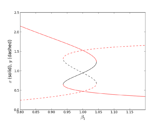
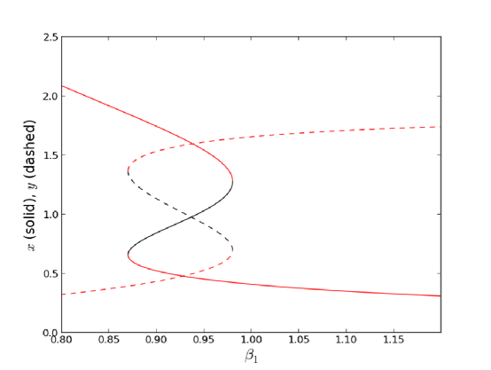
The system above may have two stable configurations in the -plane: one state has a high value of () and a low value of (); the other state has a low value of () and a high value of (). That is, the two dimensional potential underlying this system has two wells, and , in the -plane. Varying the parameters changes the depth and position of these wells, and also determines whether there are one or two wells. For example, Fig. 1 shows that for the case the system in Eqs. (2)-(3) is bistable and therefore has two stable wells only when is close to 1.
Encoding Inputs: Here the low amplitude input signal is , with equal to () if the logic input is , and being if the logic input is . So we have:
(i) corresponds to logic input set
(ii) corresponds to logic input sets /
(iii) corresponds to logic input set
Output: The outputs of the system are determined by the level of the dynamical variables and . For instance the output can be considered a logical if the state is at the high level, and logical if it is at the lower level. That is:
(i) If , then Logic Output is
(ii) If , then Logic Output is
Here is the output determination threshold that lies between the two states, e.g., at the position of the barrier between the wells. The results presented here are not sensitive to the specific value of .
Specifically, in this work, we consider the logic output to be when the state is close to the upper well, and when the state is close to the lower well, for both and variables. So when the system switches wells, the output is “flipped” or “toggled”.
The model in Eqs. (2)-(3) is based on the synthetic genetic toggle switch previously expressed in E. coli [22]. Parameter values used in [22] correspond here to , , and in Eqs. (2)-(3). By comparison, here we use , , , and . The bifurcation diagram in Fig. 1 indicates that these parameter values, along with , result in a system with a single stable well at . A non-zero input can then ”shift” the bifurcation diagram of Fig. 1 so that there is a stable state with low-, high- at .
Circuit Realization
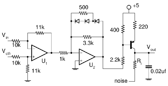
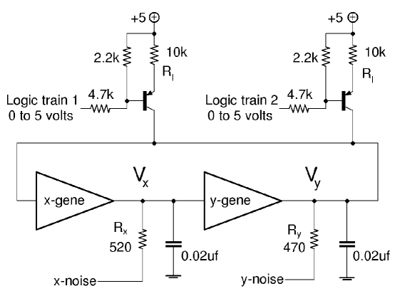
The circuit of a single inhibitory gene [24, 25] is shown in Fig. 2. The transistor current represents the rate of gene expression and the voltage represents the concentration of expressed protein. represents the concentration of repressor, and the adjusts the affinity of the repressor binding to the gene’s DNA. The Hill function inhibition in Eqs. (2)-(3) is accounted for by the dependence of the transistor current on repressor concentration voltage . The synthetic genetic network shown in Fig. 3 is comprised of two individual gene circuits connected in a loop, each inhibiting the other. For the model in Eqs. (2)-(3), the encoding inputs and add to production of which is accounted for in Fig. 3 by the two logic-driven transistors sourcing current to . Initially parameters and are taken to be zero.
The circuit equations are obtained by applying Kirchoff’s laws to and , the voltages across the capacitors in Fig. 3 [24, 25]. Multiplying both equations by results in equations for and ;
| (4) | |||||
| (5) |
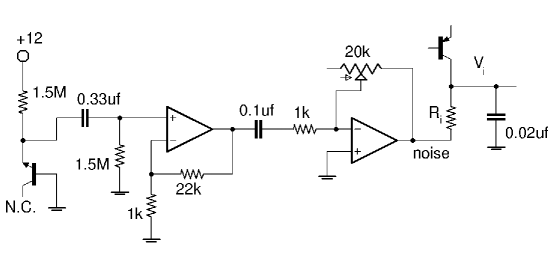
where are the Fig. 2 transistor currents for each gene, and and are currents from the logic train transistors in Fig. 3. A noise generation circuit shown in Fig. 4 based on breakdown of a reverse biased base-emitter junction produces noise with zero mean and variable amplitude. We use a well regulated supply for the noise circuit to avoid adding AC signals from the building’s electrical system into the noise. Two of these noise circuits are used to supply noisy voltages to each individual gene at locations indicated in Fig. 3.
The connections between model parameters () and circuit parameters are presented in this section using relevant numerical values, with derivations of these connections given in the next section. Readers may go directly to Results and Discussion without loss of continuity. The connections are found by relating circuit Eqs. (4)-(5) to the model Eqs. (2)-(3) and by adjusting the dependence of the transistor current on in Fig. 2 to match the Hill function inhibition. The dimensionless state-variables () in Eqs. (2)-(3) are related to voltages and by:
where corresponds to the repressor’s half-maximal inhibition binding constant . The maximal expression rate is
| (6) |
where the voltage is and . Protein decay rates are , and . The Hill coefficient comes from
| (7) |
where and are closed loop gains of U1 and U2 in Fig. 2 resulting in . The characteristic time is , so the dimensionless time is .
The high value of the encoding signals is given by
| (8) |
where is changed by varying in Fig. 3, i.e. gives . A non-zero value of in Eq. 3 is achieved in the circuit by including a third current-sourcing transistor in Fig. 3 in the same way as the two encoding signal transistors, but with the emitter resistor labelled and the input grounded so that the transistor provides a constant current . is changed by varying in the same way controls . The non-zero adds a term to Eq. 5, where
| (9) |
gives .
The terms in Eqs. (4)-(5) approximate white noise voltages. Each is characterized by its measured value and bandwidth. is controlled by changing the gain via the potentiometer in Fig. 4. Noise strength in Eqs. (2)-(3) is given by
| (10) |
where MHz is the cut-off frequency for the amplifier in Fig. 4 and decreases from at low gains to at high gain (when the potentiometer is set to in Fig. 4).
Circuit Analysis and Simulation
Here we describe the circuit analysis and derive the connections between the model parameters used in Eqs. (2)-(3) and the circuit parameters. Further details are given in Refs. [24, 25].
The single gene circuit in Fig. 2 is designed to reproduce the Hill function inhibition in Eqs. (2)-(3). The op-amp U1 is configured as a subtraction amplifier with gain . Replication of the Hill function behavior is achieved by allowing saturation of the output of the op-amp U2 and by having different unsaturated gains and for and , respectively, due to the diodes in the feedback for U2. is the gain of U2 when its output goes negative, in which case the diodes are not conducting, and therefore . is a diminishing gain when the output of U2 becomes increasingly positive causing the diodes to go into conduction. An increasing repressor concentration corresponds to surpassing which causes the unsaturated output at U2 to change from a negative voltage of to a positive voltage . The increasing voltage at the output of U2 turns the transistor off () which corresponds to complete inhibition of protein expression. Maximal protein expression in Eqs. (2)-(3) corresponds to the maximum value of , designated . occurs when (no repressor) because the output of U2 saturates at V (for the LF412 op-amp supplied by V), resulting in a 0.65 V drop across the and therefore mA.
Circuit parameters for and are found by using to convert Eqs. (4)-(5) to a dimensionless form for comparison to Eqs. (2)-(3). The used for in Eq. (6) comes from the being nearly in parallel with the resistance (10 ) at the input to the subtraction amplifier U1 for gene-. The relation for Hill coefficient is found by adjusting the dependence of on to match the slope of the Hill function at resulting in the relation [25]:
| (11) |
In Fig. 2 the voltage divider fraction and V. Using Eq. (6) in Eq. (11) yields Eq. (7).
Parameter ’s correspondence to binding affinity of repressor to DNA is seen by noting that Eqs. (2)-(3) are dimensionless, meaning that in the process of going from chemical kinetic equations to Eqs. (2)-(3) the maximal expression rate has been scaled by the repressor’s inhibition binding constant , and by a mRNA degradation rate [21, 25]. From Eq. (6) it follows that is proportional to since is inversely proportional to due to the scaling. To find the relation between in Fig. 2 and we note that the Hill function equals 0.5 when . Therefore must be half its maximum value when which gives [25]
Solving gives . Using and in Eqs. (6)-(7) gives: , satisfied by and ; V; and V.
Comparing Eqs. (3) and (5) shows that the encoding signals are related to the transistor currents by:
| (12) |
The encoding currents take on two possible values depending on whether their logic train input in Fig. 3 is high or low. When the input is high (V) the transistor is off so the current is zero. When the input is zero, the voltage divider consisting of the and produces 1Volt across the connected to the emitter of the pnp transistor creating current . Equation (12) then gives Eq. (8) for . Results of an analysis for a non-zero value of parameter are the same as for encoding signals and currents because ’s sourcing transistor is set up in the same way as the transistors in Fig. 3 for the encoding signals. Thus the non-zero value of is Eq. (9).
Here we show how to use simulations to predict the circuit results. In the process we find Eq. (10), the connection between circuit parameters and the noise strength in Eqs. (2)-(3). A standard Euler-Maruyama simulation of Eq. (2) is
| (13) |
where is a unit variance zero mean normal random distribution. The noise circuit in Fig. 4 produces a measurable rms voltage consisting of contributions from all the frequency components present in the noise. The variance of the noise is the integral of its spectral density function over frequency, and is obtained from a measurement of ;
| (14) |
Idealized white noise assumed in Eqs. (2)-(3) has a which is uniform over an infinite bandwidth. However for the real noise from the 2-stage noise amplifier circuit in Fig. 4 each op-amp’s gain-bandwidth product produces a high frequency cut-off, and . The resulting has the form
| (15) |
where is a constant related to the strength of the noise. The OPA228 op-amp has a gain-bandwidth product 33 MHz, therefore the first stage in Fig. 4 with fixed gain has cut-off, MHz. The second stage’s cut-off varies from to MHz depending on the gain setting determined by the potentiometer in the feedback of the second stage op-amp.
The integration in Eqs. (14)-(15) gives
| (16) |
There are two limiting cases for the integral: for small gains MHz giving ; and for large gain (potentiometer in Fig. 4) giving . Thus the integral in Eq. (16) is where MHz and varies from for small noise to for large noise. For frequencies within the noise bandwidth ( MHz) the amplitude spectral density (units Volt Hz-1/2) has a constant value given by
| (17) |
is a good approximation of the white noise strength provided that the Fig. 3 genetic circuit’s characteristic response rate is much less than the noise bandwidth, meaning that . This condition is ensured since the used here is , and the bandwidth of the noise is MHz.
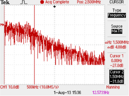
Figure 5 shows the measured frequency content from the noise circuit when the potentiometer at the second stage is set for gain producing V and MHz. In this case and . Figure 5 shows that the frequency content is relatively flat out to the cut-off near 1.5 MHz and therefore is a good approximation to white noise for the genetic network circuit. V is on the high end of the noise amplitudes used here.
The circuit Eqs. (4)-(5) which need to be simulated are of the form
| (18) |
where approximates a white noise voltage. is characterized by its measured value and bandwidth, and Eq. (17) gives the noise’s amplitude spectral density. The Euler-Maruyama simulation for Eq. 18 is
| (19) |
Using dimensionless time and the measured noise amplitude gives
| (20) |
Normalizing by the voltage scale puts Eq. (20) in the form of Eq. (13) and gives the connection between circuit parameters and dimensionless noise amplitude shown in Eq. (10). For example, using , , , and MHz gives .
Results and Discussion
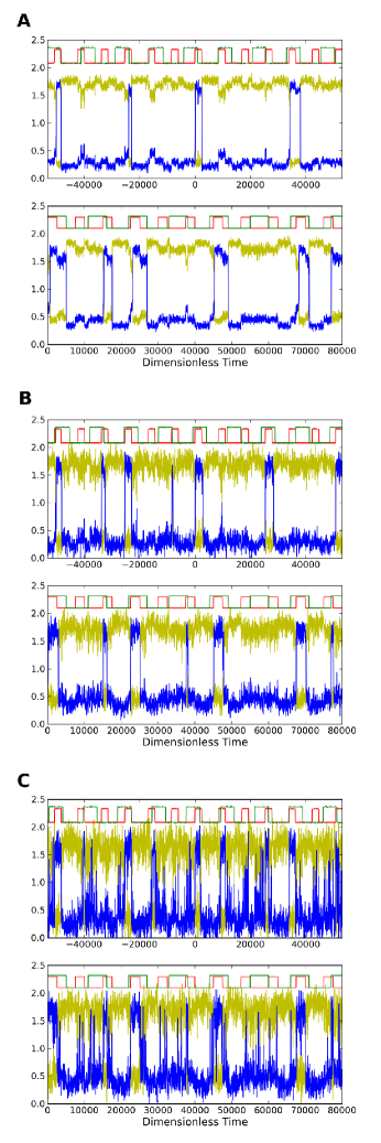
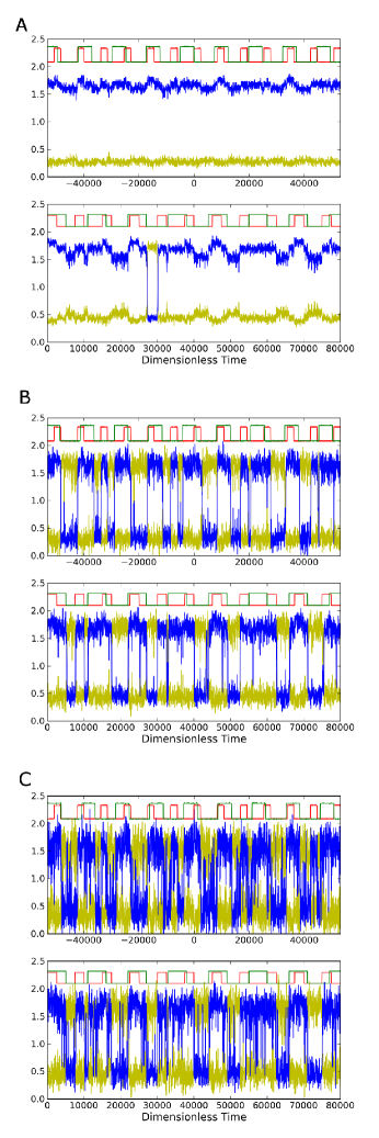
Figure 6 shows simulations and circuit measurements for three values of noise using parameters , , , , , and . It is apparent that for an optimal noise level (Fig. 6b) the circuit indeed performs the logic AND/NAND function, and that for the smaller (Fig. 6a) and larger (Fig. 6c) noise values faithful logic response is lost. At the low noise (Fig. 6a) the outputs sometimes fail to respond to the 0 to 1 transition from the AND of , and for the 1 to 0 transition the outputs often wait until both inputs go low before responding thereby causing a delayed response. In Fig. 6b the responses are quick for both the up and down transition. Figure 6c shows that at the high noise level the responses are again quick as in 6b, but the outputs also make erroneous transitions. The circuit behavior is seen to be in agreement with the simulations of Eqs. (2)-(3).
In order to investigate the range of noise strengths which produce accurate logic response, and to find optimal values for the amplitude of the small signal inputs we define an accuracy measure ,
| (21) |
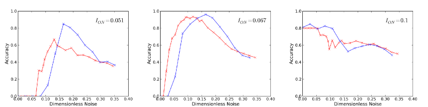
where is the percent of time the outputs are correct when the AND operation of and is low, and is the percentage of time correct when the AND operation is high. This definition has the property that when the outputs do not respond at all, then since even though . The expectation then is that for no noise there should be no stochastic resonance response so that , and that for extreme noise each accuracy would approach 50% so that . If respond immediately with no mistakes then . Figure 7 shows accuracy for simulations and circuit measurements as a function of noise strength for different values of encoding amplitude .
Figure 7a shows that for a small value of encoding amplitude, the network is not able to give a faithful logic response at any noise level. The response at low noise and at high noise are as predicted, and , respectively, but the peak of the window of stochastic resonance response is well below . Figure 7b shows a window of noise providing faithful response for . The reason that the accuracy is slightly below 1 in the window is that the outputs do not respond immediately to the AND/NAND transitions. This time lag causes the percent of time with incorrect response to be non-zero and therefore and are less than 1. In principle an allowance for a time lag could be included in the calculation of if it were deemed necessary. However, such an added complication would not make the noise window any more apparent than it already is in Fig. 7. Figure 7c shows that at a high value, , the outputs respond even with no noise, and the addition of noise only creates more errors. The relative shift between the simulation and circuit accuracies is due to assumptions made about the noise spectral density function and the integration in Eq. (16) leading to Eq. (20) which gives the connection between the measured noise amplitude and dimensionless noise . In the idealized case Eq. (16) finds ranges from to in Eq. (20), with being appropriate for the noise levels used in Fig. 6. Adjusting the value of can eliminate the relative shift, but there is nothing to be gained since the appearance of an optimal noise window for LSR at an appropriate value of is already apparent.
One can also reconfigure the system to another set of logic functions, namely the fundamental OR/NOR logic, by simply including a non-zero value for . The parameter effectively changes the relative position and depth of the wells of the bistable system, allowing the response to morph from AND/NAND to OR/NOR. For instance changing from to (with all other parameters unchanged) changes the bifurcation diagram from that in Fig. 1 to Fig. 8 showing that the system is now bistable for . The result is that the system displays a clear OR and the complementary NOR response as shown by the simulation and circuit results in Fig. 9. The low noise case Fig. 9a shows that at this low noise level the system usually fails to respond. Figure 9a also shows the resting states are reversed from the case in Fig. 6a. Figure 9b shows the OR/NOR response at a noise value within the window for LSR, and Fig. 6c shows errors when the noise is too large.
In summary, our results show that the dynamics of the two variables and with , mirror AND and the complementary NAND gate characteristics. Further, when , we obtain a clearly defined OR/NOR gate. Since is low when is high and vice-versa, the dynamics of the two variables always yield complementary logical outputs, simultaneously. That is, if operates as NAND/NOR, will give AND/OR.
These results extend the scope and indicate the generality of the recently observed phenomena of Logical Stochastic Resonance through experimental verifications. Further, these observations may provide an understanding of the information processing capacity of synthetic genetic networks, with noise aiding logic patterns. It also may have potential applications in the design of biologically inspired gates with added capacity of reconfigurability of logic operations.
We have also demonstrated that the electronic circuit provides an additional tool for investigating dynamics of proposed genetic networks. The circuit measurements are complementary to numerical simulations, thereby giving indication of the robustness of a particular network design and potential for successful realization in a biological system.
Thus the results presented in this work suggest new directions in biomolecular computing, and indicate how robust computation may be occurring at the scale of regulatory and signalling pathways in individual cells. Design and engineering of such biologically inspired computing systems not only present new paradigms of computation, but can also potentially enhance our ability to study and control biological systems [26].
Acknowledgments
S.K.D. acknowledges support by the CSIR Network project GENESIS (BC0123) and the CSIR Emeritus Scientist scheme.
References
- 1. Mano MM (1993) Computer system architecture (3. ed.). Pearson Education, I-XIII, 1-524 pp.
- 2. Bartee T (1991) Computer architecture and logic design. Computer science series. McGraw-Hill. URL http://books.google.com/books?id=b9dQAAAAMAAJ.
- 3. Bulsara A, Jacobs E, Zhou T, Moss F, Kiss L (1991) Stochastic resonance in a single neuron model: Theory and analog simulation. Journal of Theoretical Biology 152: 531 - 555.
- 4. Levin JE, Miller JP (1996) Broadband neural encoding in the cricket cereal sensory system enhanced by stochastic resonance. Nature 380: 165 - 168.
- 5. Gammaitoni L, Hänggi P, Jung P, Marchesoni F (1998) Stochastic resonance. Rev Mod Phys 70: 223–287.
- 6. Hänggi P (2002) Stochastic resonance in biology how noise can enhance detection of weak signals and help improve biological information processing. ChemPhysChem 3: 285–290.
- 7. Murali K, Sinha S, Ditto WL, Bulsara AR (2009) Reliable logic circuit elements that exploit nonlinearity in the presence of a noise floor. Phys Rev Lett 102: 104101.
- 8. Murali K, Rajamohamed I, Sinha S, Ditto WL, Bulsara AR (2009) Realization of reliable and flexible logic gates using noisy nonlinear circuits. Applied Physics Letters 95: 194102.
- 9. Guerra DN, Bulsara AR, Ditto WL, Sinha S, Murali K, et al. (2010) A noise-assisted reprogrammable nanomechanical logic gate. Nano Letters 10: 1168-1171.
- 10. Worschech L, Hartmann F, Kim TY, Hofling S, Kamp M, et al. (2010) Universal and reconfigurable logic gates in a compact three-terminal resonant tunneling diode. Applied Physics Letters 96: 042112.
- 11. Fierens P, Ibáñez S, Perazzo R, Patterson G, Grosz D (2010) A memory device sustained by noise. Physics Letters A 374: 2207 - 2209.
- 12. Sinha S, Cruz JM, Buhse T, Parmananda P (2009) Exploiting the effect of noise on a chemical system to obtain logic gates. EPL (Europhysics Letters) 86: 60003.
- 13. Singh KP, Sinha S (2011) Enhancement of “logical” responses by noise in a bistable optical system. Phys Rev E 83: 046219.
- 14. Perrone S, Vilaseca R, Masoller C (2012) Stochastic logic gate that exploits noise and polarization bistability in an optically injected vcsel. Opt Express 20: 22692–22699.
- 15. Ando H, Sinha S, Storni R, Aihara K (2011) Synthetic gene networks as potential flexible parallel logic gates. EPL (Europhysics Letters) 93: 50001.
- 16. Dari A, Kia B, Bulsara AR, Ditto W (2011) Creating morphable logic gates using logical stochastic resonance in an engineered gene network. EPL (Europhysics Letters) 93: 18001.
- 17. Dari A, Kia B, Wang X, Bulsara AR, Ditto W (2011) Noise-aided computation within a synthetic gene network through morphable and robust logic gates. Phys Rev E 83: 041909.
- 18. Sharma PR, Somani P, Shrimali MD (2013) Bio-inspired computation using synthetic genetic network. Physics Letters A 377: 367 - 369.
- 19. Hasty J, Isaacs F, Dolnik M, McMillen D, Collins JJ (2001) Designer gene networks: Towards fundamental cellular control. Chaos: An Interdisciplinary Journal of Nonlinear Science 11: 207-220.
- 20. Elowitz M, Lim WA (2010) Build life to understand it. Nature 468: 889-890.
- 21. Elowitz MB, Leibler S (2000) A synthetic oscillatory network of transcriptional regulators. Nature 403: 335-338.
- 22. Gardner TS, Cantor CR, Collins JJ (2000) Construction of a genetic toggle switch in escherichia coli. Nature 403: 339-342.
- 23. Wang J, Zhang J, Yuan Z, Zhou T (2007) Noise-induced switches in network systems of the genetic toggle switch. BMC Systems Biology 1: 50.
-
24.
Hellen EH, Volkov E, Kurths J, Dana SK (2011) An electronic analog of synthetic
genetic networks.
PLoS ONE 6: e23286.
Key: ed
Annotation: - 25. Hellen EH, Dana SK, Zhurov B, Volkov E (2013) Electronic implementation of a repressilator with quorum sensing feedback. PLoS ONE 8: e62997.
- 26. Benenson Y (2012) Biomolecular computing systems: principles, progress and potential. Nat Rev Genet 13: 455-468.
Figure Legends
Tables
| Input Set (,) | OR | AND | NOR | NAND |
|---|---|---|---|---|
| (0,0) | 0 | 0 | 1 | 1 |
| (0,1)/(1,0) | 1 | 0 | 0 | 1 |
| (1,1) | 1 | 1 | 0 | 0 |
Relationship between the two inputs and the output of the fundamental OR, AND, NOR and NAND logic operations. Note that the four distinct possible input sets , , and reduce to three conditions as and are symmetric. Note that any logical circuit can be constructed by combining the NOR (or the NAND) gates [1, 2].