Evidence for a Spin Phase Transition at in Bilayer Graphene
Abstract
The most celebrated property of the quantum spin Hall effect is the presence of spin-polarized counter-propagating edge stateskane_z_2_2005 ; bernevig_quantum_2006 ; konig_quantum_2007 . This novel edge state configuration has also been predicted to occur in graphene when spin-split electron- and hole-like Landau levels are forced to cross at the edge of the sampleabanin_spin-filtered_2006 ; fertig_luttinger_2006 ; jung_theory_2009 ; kharitonov_edge_2012 . In particular, a quantum spin Hall analogue has been predicted at in bilayer graphene if the ground state is a spin ferromagnetkharitonov_canted_2012 ; zhang_distinguishing_2012 . Previous studies have demonstrated that the bilayer state is an insulator in a perpendicular magnetic fieldfeldman_broken-symmetry_2009 ; zhao_symmetry_2010 ; weitz_broken-symmetry_2010 ; kim_spin-polarized_2011 ; velasco_jr_transport_2012 ; veligura_transport_2012 ; freitag_spontaneously_2012 , though the exact nature of this state has not been identified. Here we present measurements of the state in a dual-gated bilayer graphene device in tilted magnetic field. The application of an in-plane magnetic field and perpendicular electric field allows us to map out a full phase diagram of the state as a function of experimentally tunable parameters. At large in-plane magnetic field we observe a quantum phase transition to a metallic state with conductance of order , consistent with predictions for the ferromagnet.
Under a strong perpendicular magnetic field, bilayer graphene (BLG) develops a quantum Hall (QH) state at the charge neutrality point (CNP) which displays anomalous insulating behaviorfeldman_broken-symmetry_2009 ; zhao_symmetry_2010 ; weitz_broken-symmetry_2010 ; kim_spin-polarized_2011 ; velasco_jr_transport_2012 ; veligura_transport_2012 ; freitag_spontaneously_2012 . Transport studies in a dual-gated geometryweitz_broken-symmetry_2010 ; kim_spin-polarized_2011 ; velasco_jr_transport_2012 indicate that this gapped state results from an interaction-driven spontaneous symmetry breaking in the valley-spin spacegorbar_dynamics_2010 . However, the exact order of the resulting ground state remains controversial. In high-mobility suspended BLG devices, a broken symmetry state at charge neutrality has also been observed at zero magnetic field whose nature has been under intense theoretical castro_low-density_2008 ; lemonik_spontaneous_2010 ; vafek_many-body_2010 ; nandkishore_quantum_2010 ; kharitonov_correlated_2011 ; zhang_distinguishing_2012 and experimental mayorov_interaction-driven_2011 ; veligura_transport_2012 ; weitz_broken-symmetry_2010 ; velasco_jr_transport_2012 ; freitag_spontaneously_2012 investigation. Some experiments indicate there may be a connection between these two insulating statesvelasco_jr_transport_2012 ; freitag_spontaneously_2012 .
The state in BLG occurs at half filling of the lowest Landau level. Although the BLG zero-energy Landau level has an additional orbital degeneracy stemming from two accidentally degenerate magnetic oscillator wavefunctionsmccann_landau-level_2006 , minimization of exchange energy favors singlet pairs in the orbital space at all even filling factors barlas_intra-landau-level_2008 . This leaves an approximate SU(4) spin and pseudospin symmetry for the remaining ordering of the ground state. Comparable ground state competition has also been studied in double quantum wells in GaAs 2-dimensional electron systems (2DESs) das_sarma_double-layer_1997 . Quantum phase transitions, in particular from canted antiferromagnetic to ferromagnetic ordering, can occur in those systems as an in-plane magnetic field is applied (Zeeman energy is increased) pellegrini_evidence_1998 ; grivei_multiple_2003 .
Our experiment is carried out in BLG samples with top and bottom gates in which thin single crystal hBN serves as a high quality dielectric on both sides (Fig. 1 bottom inset). By controlling top gate voltage () and bottom gate voltage () we can adjust carrier density and perpendicular electric displacement field independently. Additionally, tilting the sample in the magnetic field allows us to independently control the Coulomb energy in a Landau level, , where the magnetic length is determined by the perpendicular magnetic field , and Zeeman energy (determined by the total magnetic field ). Since in BLG and separately couple to spin and pseudospin, respectively, our experimental setup allows us to tune anisotropies and characterize the broken-symmetry QH states in the approximate SU(4) spin-pseudospin space (see supplementary information).
Fig. 1 shows the resistance measured as a function of the two gate voltages. At zero magnetic field, the resistance at the CNP depends monotonically on due to the opening of a single particle energy gap mccann_asymmetry_2006 ; taychatanapat_electronic_2010 . With increasing applied magnetic field (Fig. 1 top inset) our device shows the same behavior reported elsewhereweitz_broken-symmetry_2010 ; velasco_jr_transport_2012 ; kim_spin-polarized_2011 , with a layer-polarized (LP) insulator (which we denote phase (i)) observed at large applied displacement field, separated from a low displacement field and high magnetic field quantum Hall insulator (phase (ii)) by a well defined boundary of finite conductance. For the remainder of the paper we focus on the behavior of phase (ii) as we vary the relative Zeeman versus Coulomb energy scales in a rotated field geometry.
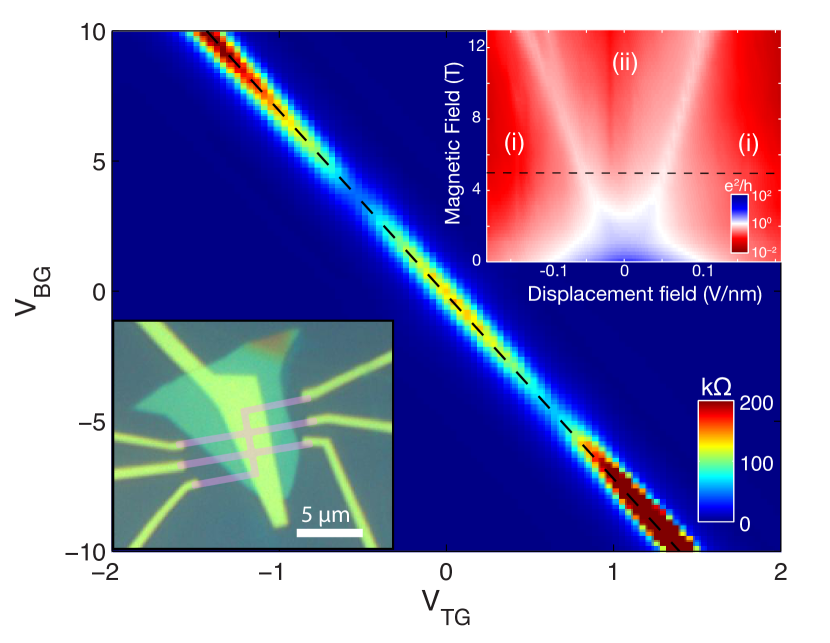
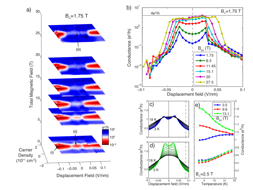
Fig. 2a shows a series of conductance maps in the vicinity of the CNP. Each pane corresponds to a fixed perpendicular applied magnetic field of 1.75 T, but with varying total field. At a total field of 1.75 T (that is, ), the distinct insulating regimes at low and high are clearly visible, as discussed in Fig. 1. At low the four-terminal conductance increases dramatically with increasing total magnetic field , reaching a value of around , after which it becomes relatively insensitive to either displacement field or magnetic field (Fig. 2b). This rapidly increasing behavior of conductance at fixed is consistent with the gradual closing of a gap in phase (ii) as increases. At fixed Coulomb energy, this decreasing gap with increasing Zeeman energy suggests that phase (ii) corresponds to a spin-unpolarized ground statefeldman_broken-symmetry_2009 ; zhao_symmetry_2010 ; veligura_transport_2012 ; kharitonov_canted_2012 . In addition, the saturation of conductance at a metallic value around at T strongly suggests a transition into a new phase with a fully closed transport gap, which we label phase (iii).
The transition between insulating and metallic behaviors can further be confirmed by investigating the temperature dependence of the conductance. Fig. 2 c and d plot four-terminal conductance at the CNP against at fixed T with T and 13.1 T, respectively. Temperature varies between 3-18 K. At small , exhibits weakly insulating behavior for , while at , metallic temperature dependence (increasing with decreasing ) is observed. Fig. 2e further contrasts the metallic versus insulating classification in different phases by plotting conductance at the CNP against temperature for both large and . shows insulating behavior for phase (ii) () and metallic behavior for phase (iii) (). At intermediate values of the conductance is relatively temperature insensitive, suggesting a gradual crossover between the two phases. Interestingly, the cusps of high conductance that mark the transition between the LP and non-LP phase show metallic temperature dependence even in a fully perpendicular field. At high (i.e. in phase (i)), the conductance remains relatively insensitive to the applied in-plane magnetic field. This is expected for a LP QH state, where the energy gap is determined by the applied displacement field.
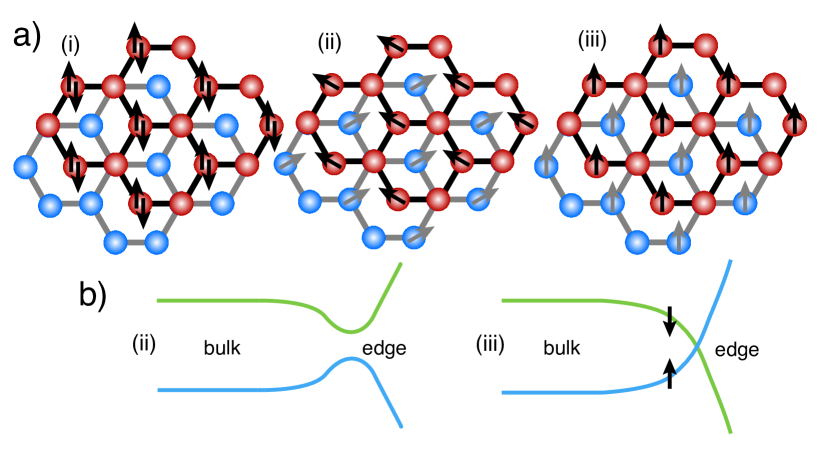
A general theoretical analysis kharitonov_canted_2012 proposes four possible ground states for in BLG: partially layer-polarized (PLP), fully layer-polarized (FLP), canted antiferromagnet (CAF), or ferromagnet (F). Considering that layer pseudospin is synonymous with sublattice and valley in the lowest Landau level mccann_landau-level_2006 , these four different scenarios can be visualized in terms of spin and sublattice of BLG (Fig. 3a). Which state the system favors depends on both anisotropies in the electron-electron and electron-phonon interactions, and external symmetry-breaking terms like Zeeman splitting and interlayer potential energy . The PLP/FLP phases are favored in the large limit, and the F phase is favored in the large limit. Unlike in GaAs double wells, these ground states may be accompanied by dramatically different transport signatures. The BLG ground state configurations discussed above are all predicted to be insulators except for the F phase. For the F phase, the highest filled band acquires an electron-like dispersion at the edge while the lowest unoccupied band acquires a hole-like dispersion (Fig. 3b)kharitonov_edge_2012 . This forces a level crossing at the edge which should result in metallic conductance of due to spin-polarized counter-propagating edge statesabanin_spin-filtered_2006 ; fertig_luttinger_2006 ; kharitonov_edge_2012 . Interpreting our results in this framework, we can identify phase (i) with either the PLP or FLP state, phase (ii) with the CAF state, and phase (iii) with the F state.
We now focus on the phase diagram of the different ground states classified above. The phase transitions between the LP, CAF, and F phases can be mapped out by locating the boundary between the metallic () and insulating () regimes as a function of and with fixed . For a given , we can define the critical displacement field for transition as the value that gives maximum change of in at fixed . Fig. 4a shows the values of and extracted from Fig. 2b ( T). In this - map three different phases can be identified, corresponding to the LP, CAF, and F phases. Note that the transition between the CAF and LP phases is sharp, as the conductance changes by an order of magnitude over a variation V/nm. By contrast the transition from CAF to F is gradual. This observation is consistent with the theoretical expectation that the LP to CAF or F transition is first order while the CAF to F transition is second orderkharitonov_canted_2012 .
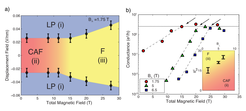
By identifying characteristic energy scales for the external symmetry breaking terms, we can comment quantitatively on the phase boundaries for a fixed . We identify Zeeman energy , where and are the electron spin g-factor and the Bohr magneton respectively, and the interlayer potential energy , where is the interlayer distance in BLG. For T, at low the CAF-LP transition occurs at meV, and at the CAF-F transition occurs at meV. The F-LP transition occurs along a line whose slope . The fact that at the F-LP phase boundary is of order unity is consistent with the increasing stability of a spin-polarized state with increasing magnetic field, providing further confirmation that the conducting phase is a ferromagnet. This observation is in qualitative agreement with theoretical predictionskharitonov_canted_2012 .
Since at the CNP and , is the only physical quantity to control the strength of e-e interactions, the phase boundary between the CAF and F phases can be further investigated by observing as a function of with different values of fixed (see supplementary information). Fig. 4b shows for three different fixed values of at . Generally, the behavior of can be characterized by two different regimes. For (i.e. the CAF phase), increases exponentially as increases. For (i.e. the F phase), is insensitive to , saturating close to . We define the critical magnetic field which separates these two regimes by the intersection of guide lines for the exponential and saturated regimes, as marked by the arrows in Fig. 3b. The identification of at different allows us to map the phase boundary between CAF and F as a function of . The inset of Fig. 4b displays as a function of . Although there are only a few data points available to indicate the phase boundary, the general trend of the CAF-F phase transition can be inferred from them.
Finally, we remark on the similarity between the F phase of BLG at and the quantum spin Hall effect (QSHE) in HgTebernevig_quantum_2006 ; konig_quantum_2007 . In the QSH phase quantized conduction is due to spin-polarized counter-propagating edge states, while the bulk remains incompressible. An analogous scenario is expected for BLG in the F quantum Hall stateabanin_spin-filtered_2006 ; fertig_luttinger_2006 ; kharitonov_edge_2012 , except that BLG carriers an additional orbital degeneracy. The F state in BL graphene is therefore expected to exhibit a four terminal conductance of , compared with for HgTe. Similar to reported measurements of HgTekonig_quantum_2007 ; roth_nonlocal_2009 , our devices show imperfect quantization with measured conductance values less than in the F phase. The reduced conductance may be due to backscattering in the edge state or through remaining impurity states in the bulk. Unambiguous experimental support for the existence of spin-polarized counter-propagating edge states should be provided by well-quantized nonlocal measurements roth_nonlocal_2009 (see supplementary information).
In conclusion, we have measured dual-gated graphene bilayers at the state. In a perpendicular magnetic field, we observe a transition between two incompressible states at a finite displacement field, indicating that the state is not layer polarized. At low displacement fields, we observe four-terminal conductance increase and then saturate as in-plane magnetic field increases, showing that the , state is also not spin polarized. This is consistent with a quantum phase transition driven by in-plane magnetic field between the canted antiferromagnet quantum Hall state and the ferromagnet. The near quantization of the 4-terminal conductance to agrees with predictions that the ferromagnetic quantum Hall ground state carries spin-polarized counter-propagating edge states.
I Methods
The device we report data from was fabricated with mechanically exfoliated graphene and hBN using a polymer membrane transfer process described in previous work dean_boron_2010 . The graphene was etched into a Hall bar pattern prior to deposition of the top hBN layer. The bottom gate is a global silicon gate, and both the contacts and the top gate are Cr/Pd/Au stacks of thickness 1/10/50 nm. Three devices fabricated in a similar way exhibited similar data trends. We present data sets obtained from the highest quality device.
These devices were measured either in a sample-in-4He-vapor variable temperature cryostat with 14 T magnet in house or in a sample-in-3He-vapor cryostat, mounted in the bore of a 31 T resistive magnet at the National High Magnetic Field Lab in Tallahassee, FL. Measurements were performed using a 1 mV voltage bias. The numerous features present in a gate voltage trace allowed precise angle calibration, with determined to better than 1% accuracy. The longitudinal resistance and Hall resistance are measured in a four-terminal geometry, so that contact resistances can be excluded. Four-terminal conductance at the CNP is obtained by taking .
II Acknowledgements
The authors thank Maxim Kharitonov for useful discussions. Portions of this experiment were conducted at the National High Magnetic Field Laboratory, which is supported by National Science Foundation Cooperative Agreement No. DMR-0654118, the State of Florida and the US Department of Energy. We thank S. Hannahs, T. Murphy, and A. Suslov for experimental assistance at NHMFL. This work is supported by AFOSR MURI. PM acknowledges support from ONR MURI and FENA. AFY and PK acknowledge support from DOE (DE-FG02-05ER46215) for carrying out experiments and INDEX for sample fabrication.
III Contributions
PM, CRD, and AFY designed and conceived the experiment. TT and KW synthesized hBN samples, PM fabricated the samples. PM, CRD, and AFY performed the measurements. PM, CRD, and PK analyzed the data and wrote the paper. JH, KS, and PK advised on experiments.
References
- (1) Kane, C. L. & Mele, E. J. Z2 topological order and the quantum spin Hall effect. Physical Review Letters 95 (2005).
- (2) Bernevig, B. A., Hughes, T. L. & Zhang, S.-C. Quantum spin Hall effect and topological phase transition in HgTe quantum wells. Science 314, 1757 –1761 (2006).
- (3) König, M. et al. Quantum spin Hall insulator state in HgTe quantum wells. Science 318, 766 –770 (2007).
- (4) Abanin, D. A., Lee, P. A. & Levitov, L. S. Spin-filtered edge states and quantum Hall effect in graphene. Physical Review Letters 96, 176803 (2006).
- (5) Fertig, H. A. & Brey, L. Luttinger liquid at the edge of undoped graphene in a strong magnetic field. Physical Review Letters 97, 116805 (2006).
- (6) Jung, J. & MacDonald, A. H. Theory of the magnetic-field-induced insulator in neutral graphene sheets. Physical Review B 80, 235417 (2009).
- (7) Kharitonov, M. Edge excitations of the canted antiferromagnetic phase of the quantum Hall state in graphene: A simplified analysis. Physical Review B 86, 075450 (2012).
- (8) Kharitonov, M. Canted antiferromagnetic phase of the quantum Hall state in bilayer graphene. Physical Review Letters 109, 046803 (2012).
- (9) Zhang, F. & MacDonald, A. H. Distinguishing spontaneous quantum Hall states in bilayer graphene. Physical Review Letters 108, 186804 (2012).
- (10) Feldman, B. E., Martin, J. & Yacoby, A. Broken-symmetry states and divergent resistance in suspended bilayer graphene. Nat Phys 5, 889–893 (2009).
- (11) Zhao, Y., Cadden-Zimansky, P., Jiang, Z. & Kim, P. Symmetry breaking in the zero-energy Landau level in bilayer graphene. Physical Review Letters 104, 066801 (2010).
- (12) Weitz, R. T., Allen, M. T., Feldman, B. E., Martin, J. & Yacoby, A. Broken-symmetry states in doubly gated suspended bilayer graphene. Science 330, 812 –816 (2010).
- (13) Kim, S., Lee, K. & Tutuc, E. Spin-polarized to valley-polarized transition in graphene bilayers at in high magnetic fields. Physical Review Letters 107, 016803 (2011).
- (14) Velasco Jr, J. et al. Transport spectroscopy of symmetry-broken insulating states in bilayer graphene. Nature Nanotechnology 7, 156–160 (2012).
- (15) Veligura, A. et al. Transport gap in suspended bilayer graphene at zero magnetic field. Physical Review B 85, 155412 (2012).
- (16) Freitag, F., Trbovic, J., Weiss, M. & Schönenberger, C. Spontaneously gapped ground state in suspended bilayer graphene. Physical Review Letters 108, 076602 (2012).
- (17) Gorbar, E. V., Gusynin, V. P. & Miransky, V. A. Dynamics and phase diagram of the quantum Hall state in bilayer graphene. Physical Review B 81, 155451 (2010).
- (18) Kharitonov, M. Correlated antiferromagnetic state in bilayer graphene. arXiv:1109.1553 (2011).
- (19) Lemonik, Y., Aleiner, I. L., Toke, C. & Fal’ko, V. I. Spontaneous symmetry breaking and Lifshitz transition in bilayer graphene. Physical Review B 82, 201408 (2010).
- (20) Vafek, O. & Yang, K. Many-body instability of Coulomb interacting bilayer graphene: Renormalization group approach. Physical Review B 81, 041401 (2010).
- (21) Nandkishore, R. & Levitov, L. Quantum anomalous Hall state in bilayer graphene. Physical Review B 82, 115124 (2010).
- (22) Castro, E. V., Peres, N. M. R., Stauber, T. & Silva, N. A. P. Low-density ferromagnetism in biased bilayer graphene. Physical Review Letters 100, 186803 (2008).
- (23) Mayorov, A. S. et al. Interaction-driven spectrum reconstruction in bilayer graphene. Science 333, 860 –863 (2011).
- (24) McCann, E. & Fal’ko, V. I. Landau-level degeneracy and quantum Hall effect in a graphite bilayer. Physical Review Letters 96, 086805 (2006).
- (25) Barlas, Y., Côté, R., Nomura, K. & MacDonald, A. H. Intra-Landau-level cyclotron resonance in bilayer graphene. Physical Review Letters 101, 097601 (2008).
- (26) Das Sarma, S., Sachdev, S. & Zheng, L. Double-layer quantum Hall antiferromagnetism at filling fraction where is an odd integer. Physical Review Letters 79, 917–920 (1997).
- (27) Pellegrini, V. et al. Evidence of soft-mode quantum phase transitions in electron double layers. Science 281, 799–802 (1998).
- (28) Grivei, E., Melinte, S., Bayot, V., Manoharan, H. C. & Shayegan, M. Multiple interacting bilayer electron system: Magnetotransport and heat capacity measurements. Physical Review B 68, 193404 (2003).
- (29) McCann, E. Asymmetry gap in the electronic band structure of bilayer graphene. Physical Review B 74, 161403 (2006).
- (30) Taychatanapat, T. & Jarillo-Herrero, P. Electronic transport in dual-gated bilayer graphene at large displacement fields. Physical Review Letters 105, 166601 (2010).
- (31) Roth, A. et al. Nonlocal transport in the quantum spin Hall state. Science 325, 294 –297 (2009).
- (32) Dean, C. R. et al. Boron nitride substrates for high-quality graphene electronics. Nat Nano 5, 722–726 (2010).