Gate-tuned Differentiation of Surface-conducting States in Bi1.5Sb0.5Te1.7Se1.3 Topological-insulator Thin Crystals
Abstract
Using field-angle, temperature, and back-gate-voltage dependence of the weak anti-localization (WAL) and universal conductance fluctuations of thin Bi1.5Sb0.5Te1.7Se1.3 topological-insulator single crystals, in combination with gate-tuned Hall resistivity measurements, we reliably separated the surface conduction of the topological nature from both the bulk conduction and topologically trivial surface conduction. We minimized the bulk conduction in the crystals and back-gate tuned the Fermi level to the topological bottom-surface band while keeping the top surface insensitive to back-gating with the optimal crystal thickness of 100 nm. We argue that the WAL effect occurring by the coherent diffusive motion of carriers in relatively low magnetic fields is more essential than other transport tools such as the Shubnikov-de Hass oscillations for confirming the conduction by the topologically protected surface state. Our approach provides a highly coherent picture of the surface transport properties of TIs and a reliable means of investigating the fundamental topological nature of surface conduction and possible quantum-device applications related to momentum-locked spin polarization in surface states.
pacs:
73.20.At,73.25.+i,73.23.-b,72.20.-iI Introduction
Similar to an ordinary-band insulator, a topological insulator (TI) has a bulk energy gap in its band structure, which is generated by a strong spin-orbit interaction. The topological phase transition, brought about by the band inversion in the material, induces Dirac-fermionic surface-conducting channels. Fu and Kane (2007); Fu et al. (2007); Zhang et al. (2009a); Hasan and Kane (2010); Qi and Zhang (2011) This topologically protected surface state (TSS) has a helical spin texture that is robust to small perturbations conserving the time-reversal symmetry, and thus prohibiting backscattering by nonmagnetic impurities. Roushan et al. (2009); Zhang et al. (2009b); Alpichshev et al. (2010)
Diverse transport studies were conducted to characterize the TSS. In general, however, as-grown TIs are - or -doped so that the surface conduction can be predominated by bulk conduction. Xia et al. (2009); Chen et al. (2009); Hsieh et al. (2009) Efforts have been made to reduce the bulk conduction by tuning the Fermi level () into the bulk band gap. Chen et al. (2009); Hsieh et al. (2009); Ren et al. (2011a); Taskin et al. (2011); Arakane et al. (2012); Ren et al. (2012); Chen et al. (2010); Checkelsky et al. (2011); Kim et al. (2012); Steinberg et al. (2010); Kong et al. (2011); Hong et al. (2012); Wang et al. (2012) Even with these efforts, however, critical inconsistencies were present in the previous transport measurements. For instance, in bulk TIs with a thickness larger than m, two-dimensional (2D) Shubnikov-de Haas oscillations (SdHO) were observed. Nonetheless, the weak anti-localization (WAL) effect, relevant to the TSS, was often absent in the corresponding measurements, or, if present, did not fit well to the 2D Hikami-Larkin-Nagaoka (HLN) WAL expression Analytis et al. (2010a); Eto et al. (2010); Analytis et al. (2010b); Ren et al. (2010); Petrushevsky et al. (2012); Xiong et al. (2012a); Qu et al. (2010); Ren et al. (2011b, 2012); Checkelsky et al. (2009); Hikami et al. (1980) (see Appendix A). In a TI, the WAL effect is generated by a strong spin-orbit interaction and the consequent destructive interference between two electron waves traveling along a diffusive closed path in a time-reversal manner. Anderson (1958); Hikami et al. (1980); Bergmann (1984)
These inconsistencies between the 2D SdHO and WAL were also observed in thinner flakes, with a thickness less than m. Hong et al. (2012); Wang et al. (2012); Xiu et al. (2011); He et al. (2012) Furthermore, previous 2D-SdHO observations Ren et al. (2012); Wang et al. (2012); Analytis et al. (2010b); Ren et al. (2010); Petrushevsky et al. (2012); Xiong et al. (2012a); Xiu et al. (2011); He et al. (2012) may not have been fully relevant to the surface conduction by the TSS. Petrushevsky et al. (2012); Cao et al. (2012); Xiong et al. (2012b) Accurately identifying the Berry-phase shift associated with the TSS requires measurements in very strong magnetic fields, with careful Landau-level indexing. Xiong et al. (2012b) In most of the previous studies, however, the Berry-phase shift was determined based on observations in relatively weak magnetic fields. Ren et al. (2012); Wang et al. (2012); Ren et al. (2010); Xiong et al. (2012a); Xiu et al. (2011); He et al. (2012) Ambipolar characters with back-gating were also observed in the transport of TIs, which were assumed to be associated with the TSS. Here, however, the WAL effect was absent in the samples with relatively high carrier densities. Steinberg et al. (2010); Kong et al. (2011); Hong et al. (2012) The WAL effect observed in some of these ambipolar-transport samples were reported to arise from the coupling between the surface and the bulk bands, rather than the TSS exclusively. Chen et al. (2010); Checkelsky et al. (2011); Kim et al. (2012); Chen et al. (2011); Kim et al. (2011a); Matsuo et al. (2012); Steinberg et al. (2011); Zhang et al. (2011); Cha et al. (2012)
It is an extremely difficult task to reliably separate the TSS from other conductance contributions. In this study, we minimized the bulk conduction using high-quality Bi1.5Sb0.5Te1.7Se1.3 (BSTS) TI single crystals, with lying in the bulk gap without gating. We confirmed that the WAL effect and universal conductance fluctuations (UCF) indeed arose from the top and bottom surfaces. By back-gate tuning the WAL characteristics, we identified the TSS conducting characteristics and the coupling between the TSS and the topologically trivial two-dimensional electron gas (2DEG) states that emerged due to band bending near the bottom surface. The ambipolar Hall resistivity of the bottom surface was consistent with the back-gate-voltage () dependence of the longitudinal resistance of the TSS. This study provides a reliable means of differentiating the TSS of TIs from those of the bulk conducting state and the topologically trivial 2DEG states, along with a highly coherent picture of the topological surface transport properties of TIs.
II Sample preparation and measurements
BSTS single crystals were grown using the self-flux method. Taskin et al. (2011); Ren et al. (2011a) Stoichiometric mixture of high-purity starting materials (Bi(5N), Sb(5N), Te(5N), Se(5N)) were loaded in an evacuated quartz ampoule, which was then heated up to 850 ∘C. After annealing at 850 ∘C for 2 days to enhance the material homogeneity, the melt mixture was slowly cooled down to 600 ∘C for a week. Before complete furnace cooling it was kept at 600 ∘C for one more week to further improve the crystallinity. The stoichiometry and the high crystallinity of the single crystals were confirmed by the energy dispersive spectroscopy and the x-ray diffraction, respectively.
The bulk transport properties were examined using 100 m-thick cleaved bulk crystals. For detailed characterization of transport properties with back-gating, BSTS flakes, which are 22 to 230 nm in their thickness, were mechanically exfoliated onto a Si substrate capped with a 300-nm-thick oxidized layer. This was then followed by standard electron (e)-beam patterning and e-gun evaporation of Ti/Au (10 nm/100350 nm thick) bilayer electrodes and contact leads. For thick crystals, the electrode contacts were prepared using silver paste. In total, four thick bulk crystals and six thin flakes were investigated using standard lock-in measurements, varying from 290 to 4.2 K.
III Results and discussion
III.1 Thickness and temperature dependence of resistance
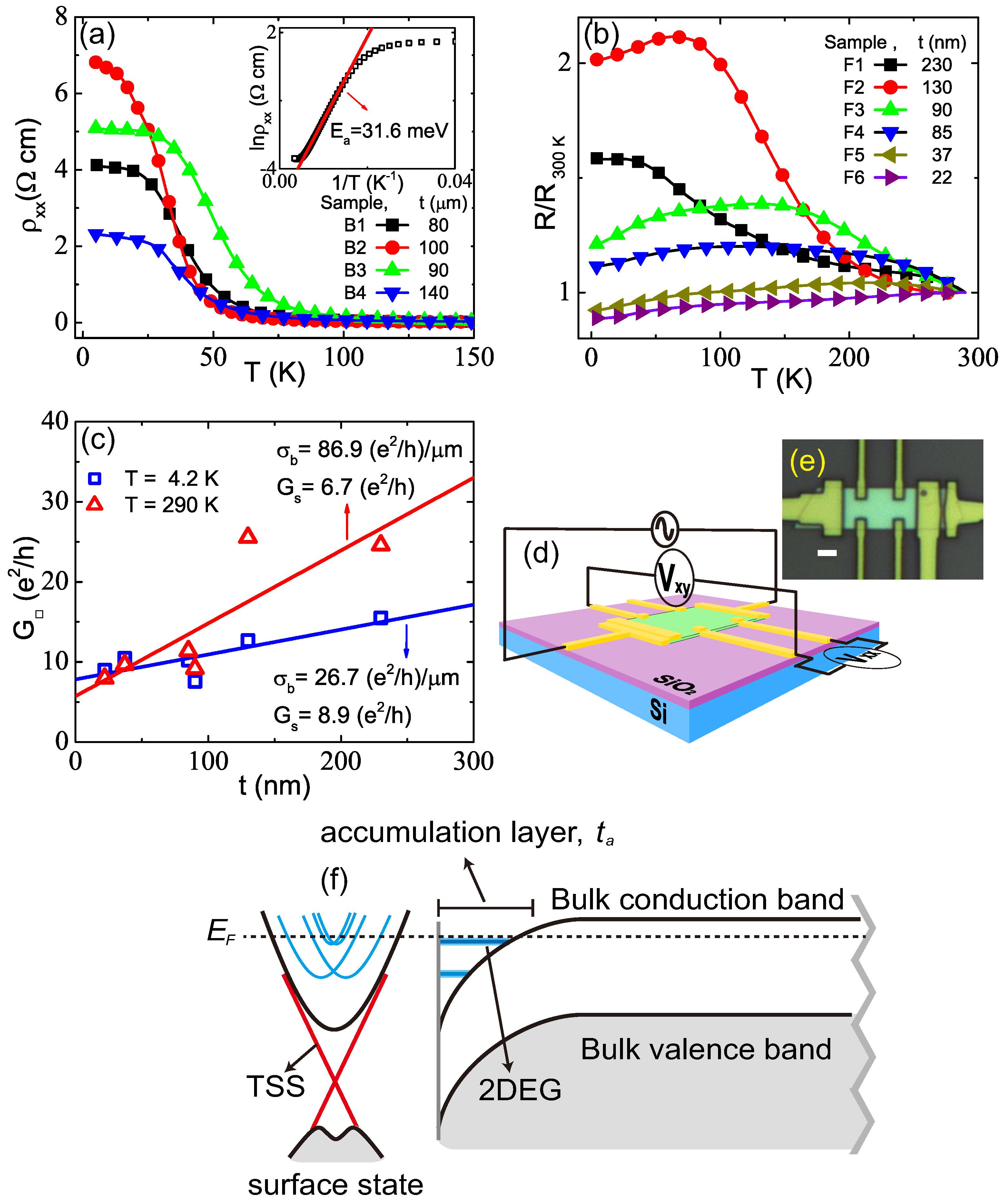
The dependence of the resistivity of the thick bulk crystals of BSTS in Fig. 1(a) exhibits conventional semiconducting behavior down to K. A fit of to the Arrhenius law renders the activation energy of 26.1, 21.3, 31.6 and 20.7 meV for samples B1, B2, B3 and B4 (inset in Fig. 1(a) corresponds to sample B3), consistent with previous studies. Arakane et al. (2012) However, the resistance is saturated for below K, which indicates the emergence of additional conducting channels. This behavior was more pronounced in the thin flakes. Figure 1(b) shows a clear semiconductor-metal transition as the thickness of the flakes decreases. The variation of with the flake thickness can be interpreted in terms of surface-conducting channels in the presence of a bulk insulating gap, as illustrated in Fig. 1(f). With inside the bulk energy gap, the residual bulk conduction by carriers thermally activated from an impurity band was dominant in the thick crystals (Fig. 1(a)). Thin flakes, however, with less bulk conductance, exhibited metallic behavior. One can confirm this behavior by modelling the simple form for total sheet conductance as follows:
| (1) |
where is the surface sheet conductance, is the bulk conductivity, and is the thickness of crystals. Here, includes the conduction through the 2DEG layer (see Fig. 1(f)) in the potential well formed by surface band bending, as well as the conduction by the TSS. Bianchi et al. (2010); King et al. (2011); Benia et al. (2011) Fitting the observed results to Eq. (1) (Fig. 1(c)), is estimated to be and m-1 at 290 and 4.2 K, respectively. These values are at least two orders of magnitude smaller than the ones reported previously for Bi2Se3, Steinberg et al. (2010) indicating that our BSTS single crystals were highly “bulk-insulating”. Assuming the range of surface band bending at the surface to be 30 nm (see Appendix B) in sample F4, the relative weight of the bulk to the surface conductance becomes () at 290 K (4.2 K).
III.2 Angle and temperature dependence of WAL and UCF
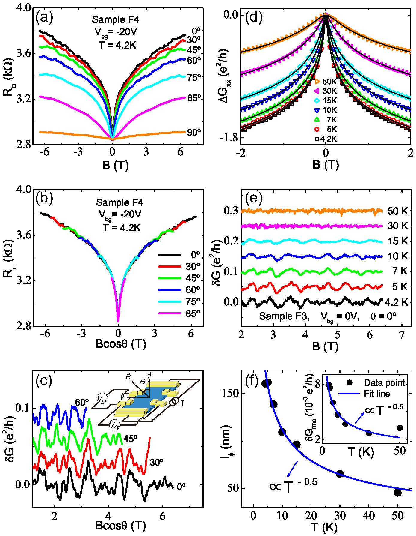
The surface-dominant conduction at low becomes more evident in the field-angle dependence of the magnetoresistance (MR). Figure 2(b) shows that all of the MR curves taken at different field angles (Fig. 2(a)), plotted as a function of the normal component of the field (B⊥), merge into a single universal curve (see Appendix C for the discussion on the MR feature in in-plane fields; =90∘). Even the positions of the UCF peaks agree with each other when plotted as a function of B⊥ (Fig. 2(c)). These features strongly indicate that the MR in our sample was almost completely dominated by surface conduction over the entire field range of our measurements. Previously, the cos() angle dependence of the MR was observed only in the low-field range of within a fraction of tesla. Cha et al. (2012); He et al. (2011)
The 2D nature was identified more quantitatively from the dependence of the MR. Figure 2(d) is the dependence of WAL effects and the best fits of to Eq. (2), from which we obtained the dependence of the phase relaxation length as shown in Fig. 2(f) (more details of the WAL effect are discussed below). Figure 2(e) shows the dependence of , with the corresponding dependence of the UCF amplitude shown in the inset of Fig. 2(f). In a 2D system with a sample dimension of , scales as for inelastic scattering by electron-electron interaction, and is proportional to . Choi et al. (1987); Altshuler et al. (1982); Lee and Stone (1985); Lee et al. (1987) In Fig. 2(f), both and scale as , in good agreement with the theoretical predictions, indicating that the dominant inelastic scattering in the surface-conducting channels of our BSTS flakes was due to the electron-electron interaction.
III.3 Back-gate dependence of WAL
Up to this point, results from our BSTS consistently indicate that the bulk conduction was negligible, and that both WAL and UCF had a 2D nature. The WAL in the TSS arose from the Berry phase caused by the helical spin texture. Since the Rashba-split 2DEG has the momentum-locked spin helicity (see Figs. 3(d), (e), and (f)), the topologically trivial 2DEG states also exhibit the WAL effect. Applying , we confirmed that the WAL effect arose from surface conduction, in both TSS and the topologically trivial 2DEG, with negligible bulk conduction. According to the HLN theory, for a 2D system in the symplectic limit, i.e., in the limit of strong spin-orbit coupling (; is the dephasing time, the spin-orbit scattering time, and the elastic scattering time) with a negligible Zeeman term, the magnetoconductance correction is given as follows:
| (2) |
where is the digamma function, is the electronic charge, is Planck’s constant divided by , and is the phase-relaxation length. Hikami et al. (1980) Because the WAL effect constitutes a prominent transport property of the TSS, the relationship between the parameter and the number of conducting channels in the symplectic limit is essential to differentiating the transport nature of TIs. Garate and Glazman (2012) Each 2D conducting channel in the symplectic limit contributes 0.5 to the value of . If there are two independent 2D conducting channels in the symplectic limit, (, corresponding to the channel ) and is replaced by the effective phase relaxation length (see Appendix D for details of the WAL fitting).
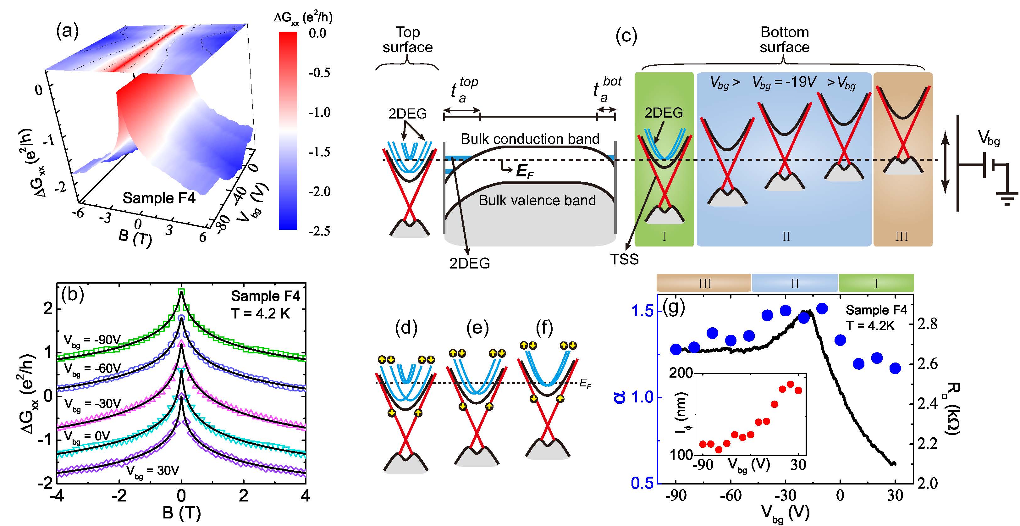
We confirmed that the back-gating affected only the bottom-surface conductance for the 8590 nm-thick samples (F3 and F4) (see Appendix E). Figure 3(a) shows vs in color codes (online) as a function . Here, the WAL effect occurs over the entire range of of this study with a maximum at V, the Dirac point of the TSS at the bottom surface (corresponding to the center diagram in Region II of Fig. 3(c)). Figure 3(b) shows curves for different values of , which agree well with Eq. (2) (solid curves) over the entire range of ; the corresponding values of are plotted in Fig. 3(g). For all , exceeds unity, indicating that more than two 2D conducting channels with the symplectic-limit behavior were involved in the surface conduction.
In Region II of Fig. 3(g), the TSS in the bottom surface contributes a value of 0.5 to . This leaves for the top surface, which does not appear to be affected by . Thus, we infer that the band bending near the top surface is like what is shown in Fig. 3(c). In the top surface, in addition to the TSS, the two Rashba-split channels in the trivial 2DEG layer also exhibit WAL in the symplectic limit. Bianchi et al. (2010); King et al. (2011); Benia et al. (2011) However, the magnitude of is reduced from 1.5 (=0.53) to 1 due to inter-band scattering, where the degree of reduction depends on the scattering strength. Garate and Glazman (2012) In Region I, also enters the bulk conduction band (BCB) of the bottom surface. But, if the surface band bending is not enough to make a sufficient Rashba splitting in the 2DEG states as in Fig. 3(f), the band structure of the 2DEG would be similar to the unitary case, Hikami et al. (1980) where the scattering between the TSS and the topologically trivial 2DEG states is enhanced along with weakening of the WAL effect. Lu and Shen (2011) This reduces the value of of the bottom surface down to , while leaving unchanged at for the top surface. If is shifted deeper into the conduction band as to form a 2DEG on the bottom surface with a large-Rashba-split bulk subband (Fig. 3(d)), the WAL effect will be enhanced again, with the value of larger than 0.5 as shown in Fig. 3(c) for the top surface. Garate and Glazman (2012) In Region III, a similar reduction of is expected for the bottom surface, due to the enhanced scattering between the TSS and the bulk valence band (BVB). Thus, the variation of with in Fig. 3(g) is the result of variation of the WAL in the bottom surface state.
The WAL effects reported previously on TIs with Chen et al. (2010); Kim et al. (2012); Chen et al. (2011); Kim et al. (2011a); Matsuo et al. (2012) or Checkelsky et al. (2011); Hong et al. (2012); Steinberg et al. (2011); Zhang et al. (2011); Cha et al. (2012); Gao et al. (2012) contained a finite bulk contribution. corresponded to an effective single layer formed by the bulk and the two (top and bottom) surfaces, which are strongly coupled together. Meanwhile, corresponded to an effective single layer formed by the -type bulk strongly coupled to the top surface, in association with the -type bottom surface that was decoupled from the bulk by the formation of the depletion layer for a large negative value of . Garate and Glazman (2012) To the best of our knowledge, no previous reports have shown good fits to the symplectic-limit expression of Eq. (2) for fields up to several tesla, with exceeding unity. Chen et al. (2010); Checkelsky et al. (2011); Hong et al. (2012); Kim et al. (2012); Chen et al. (2011); Kim et al. (2011a); Matsuo et al. (2012); Steinberg et al. (2011); Zhang et al. (2011); Cha et al. (2012); Gao et al. (2012) Although the good fits of our results to Eq. (2) without the Zeeman correction may be related to the recent report of small Landé factor in TIs, Xiong et al. (2012b); Cheng et al. (2010); Hanaguri et al. (2010) more studies are required to draw a definite conclusion on the issue.
III.4 Back-gate dependence of Hall resistivity
From the thickness, field-angle, and temperature dependence of the resistance, we conclude that in our BSTS samples the electronic transport was dominated by the top and bottom surfaces. In this case, the Hall resistivity can be described by a standard two-band model as Ashcroft and Mermin (1976)
| (3) |
Here, and are the density and mobility of the carriers, respectively, in the -th conducting channel. The top (=1) and bottom (=2) surfaces constitute parallel conducting channels, with being positive (negative) for -type (-type) carriers. Ashcroft and Mermin (1976) In sufficiently strong fields, converges to . In weak fields ( T), Eq. (3) is reduced to
| (4) |
Here, the double signs are of the same order. The upper (lower) sign corresponds to ().
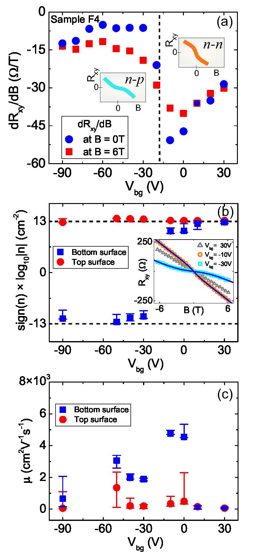
Figure 4(a) shows the results of analysis of the dependence of Hall resistivity from sample F4. For V, the difference between the square (red online) and the circle (blue online), which means nonlinearity of , is very small, thus the curves are almost linear in . As the is lowered to a negative value, the curves starts to bend and the nonlinearity of the increases as the decreases (curve in right inset in Fig. 4(a)). In this region (e.g. V), the slope of the tangent to at T is larger than that at T. However, the feature is reversed for 30 V (curve in left inset in Fig. 4(a)) and the nonlinearity of decreases as the decreases. Using Eq. (4), it turned out that the change in the shape of the curve (from right inset to left inset in Fig. 4(a)) indicates the ambipolar transport of Dirac fermions between the - state (top: -doped, bottom: -doped) and the - state on TI surfaces.
If and in Eq. (4), then , corresponding to the region of 15 V in Fig. 4(a). Since the curves are almost linear in , the carrier mobility is estimated to be , cm2/(Vs) using the relationship , which agrees with previous reports. Taskin et al. (2011); Xiong et al. (2012a, b) In this region (Region I in Fig. 3(c)) with in the BCB, the mobility decreased due to the enhanced inter-band scattering. Bianchi et al. (2010) As decreased, with shifted to the TSS in Region II in Fig. 3(c), the mobility of the bottom surface was enhanced so that . In this case, if , Eq. (4) leads to , which corresponds to the curve for V in the inset of Fig. 4(b) (right inset in Fig. 4(a)). Decreasing further, shifted to a -type region at the bottom surface. With and , Eq. (4) leads to , corresponding to the curve for V in the inset of Fig. 4(b) (left inset in Fig. 4(a)). The change in the relative magnitude of the slopes of the tangent to , i.e., and , for crossing V clearly indicates ambipolar transport of the Dirac fermions between the - and - states on the TI surface. For V (Region III in Fig. 3(c)), with in the BVB, scattering between the TSS and the BVB was enhanced once again. Kim et al. (2011b) The resulting suppression of , combined with an increase of in the range of V along with the relationship for the bottom surface, may explain the low sensitivity of to in Fig. 3(g).
Fitting the data to Eq. (3) gives more quantitative support for the analysis above on the dependence of the Hall resistivity. The inset of Fig. 4(b) shows the representative Hall resistivity for 30, , and V, where the solid curves are the best fits to Eq. (3) with the parameter values summarized in Figs. 4(b) and (c). in Fig. 4(b) is almost constant for all values of , while changes its sign between and types at V. This indicates ambipolar transport for the bottom surface with varying across the Dirac point, while the top surface remained mostly unaffected by back-gating, consistent with earlier qualitative analysis of dependent Hall resistivity. This back-gating effect on the two surfaces was also confirmed by the mobility change. In Fig. 4(c), the best-fit values of are almost insensitive to the variation of . However, turns out to be significantly larger than in the region, 50 V0 V, where is assumed to be in the Dirac band of the bottom surface. The enhancement possibly stems from the mobility increase as shifts into the Dirac band of the bottom surface from the trivial 2DEG band (either conduction or valence), where is reduced by the scattering between the TSS and the trivial 2DEG band. It should be noted that, with the invasive configuration of electrodes adopted in this study, the observed Hall voltage is bound to be underestimated. However, the qualitative dependence of the parameters in Eq. (3) remains valid.
IV Conclusion
The Berry-phase shift in SdHO is often adopted to examine the topological nature of surface transport. However, very strong magnetic fields of 50 T with careful Landau-level indexing, required for accurate determination of the Berry phase, have made it difficult to clearly differentiate the conductance by the TSS from that by the trivial 2D-conducting states. Observation of SdHO also requires relatively high mobility with a sufficiently long mean-free path to support the cyclotron orbital motion. In contrast, the observation of WAL, an intrinsic 2D effect, directly points to conduction by the TSS. Furthermore, WAL, which arises from the coherent diffusive motion of carriers, is not limited to the high mobility state. In this sense, the WAL effect which was used primarily in this study can be considered to be a more essential criterion than the SdHO for confirming the conduction by the TSS.
For flakes significantly thicker than an optimum thickness of 8090 nm, the bulk conductance cannot be neglected. On the other hand, as the range of band bending near the top and bottom surfaces begins to overlap for thinner flakes, independent gate control of the surface conduction would no longer be possible. Thus, our approach of separating the TSS by examining the transport characteristics specific to the 2D-topological nature in the optimal-thickness crystal flakes (in combination with back-gating) provides a convenient means of investigating the fundamental topological nature of the surface conduction and the quantum-device applications associated with momentum-locked spin polarization in the surface state of TIs.
Acknowledgements.
HJL thanks V. Sacksteder for valuable discussion on the in-plane MR. This work was supported by the National Research Foundation (NRF), through the SRC Center for Topological Matter [Grant No. 2011-0030788 (for HJL) and 2011-0030785 (for JSK)], the GFR Center for Advanced Soft Electronics (Grant No. 2011-0031640; for HJL), and the Mid-Career Researcher Program (Grant No. 2012-013838; for JSK).Appendix A Possible formation of multiple parallel 2D conducting channels in TIs
The weak anti-localization (WAL) in bulk topological insulator (TI) single crystals and thin TI flakes with high carrier density was reported previously. Checkelsky et al. (2009); Analytis et al. (2010b); Wang et al. (2012) However, the magnitude of the consequent conductance correction () was larger than our results by one or two orders of magnitude. Since the magnitude of is proportional to the parameter in Eq. (2) in the main text, which corresponds to the number of parallel conducting channels, one may suspect that multiple two-dimensional (2D) conducting channels connected in parallel were present for the conduction of TI in previous studies. A recent report Cao et al. (2012) supports the inference. In Ref. [Cao et al., 2012], it was concluded that the observed quantized Hall effect and SdHO were not caused by the topologically protected surface state (TSS) but by many topologically trivial 2D conducting channels connected in parallel.
From the SdHO measurements, one can obtain the information on the dimensionality and carrier density of the conducting channels. In the SdHO analysis, the degeneracy “2” corresponds to the bulk band or the topologically trivial two-dimensional electron gas (2DEG) on the surface accumulation layer, while the degeneracy “1” corresponds to the TSS. In some previous studies, Lang et al. (2012); Petrushevsky et al. (2012) the carrier density was estimated from the SdHO data adopting the degeneracy ‘1’ under the assumption that the observed SdHO arose from the TSS. The carrier density estimated in this way was claimed to be relevant to the TSS, based on the fact that, with lying in the TSS, the maximum carrier density is expected to be depending on the TI materials used. However, if the SdHO had arisen from the topologically trivial 2D conducting channels, the degeneracy should have been ‘2’ with a doubled carrier density. In this case, however, a Dirac cone cannot accommodate all the carrier states estimated with the degeneracy ‘2’ in Ref. [Petrushevsky et al., 2012] and [Lang et al., 2012] without the bulk conduction band or 2DEG states.
In fact, the SdHO frequencies themselves obtained in Ref. [Cao et al., 2012] and Refs. [Petrushevsky et al., 2012, Lang et al., 2012] were not much different from each other. Thus, the difference in the carrier densities between Ref. [Cao et al., 2012] and Refs. [Petrushevsky et al., 2012, Lang et al., 2012] resulted from the different degeneracy values adopted in the analysis. Depending on the degeneracy value used in the SdHO analysis, one may reach very different conclusions on the topological nature of the conducting channels involved in the SdHO data. In this sense, observation of the SdHO itself cannot confirm the existence of the TSS. Correctly identifying the Berry phase in strong magnetic fields is essential to confirming the TSS in TIs. Xiong et al. (2012b)
Appendix B Surface band bending
The surface band bending effect is a common feature of semiconductors. In particular, for narrow-gap semiconductors, the transport and electronic contact properties are strongly affected by the surface band bending. The materials which are identified as TIs are, in general, narrow-gap semiconductors whose band gap is about . Zhang et al. (2009a) Since the energy levels of the surface state can be shifted up to a few hundred meV, King et al. (2011); Benia et al. (2011); Chen et al. (2012) the surface band bending has a large influence on transport properties of TIs. But, it has not been studied in depth to date.
The depth of the surface accumulation layer ( in Fig. 1(f) in main text) depends on the distribution of the local carrier density along the -axis. Ando et al. (1982); Fowler (1975) For samples with the relatively high carrier density, i.e., if lies in the bulk conduction band, was calculated to be nm. Wang et al. (2012); King et al. (2011); Benia et al. (2011); Bianchi et al. (2010); Xiu et al. (2011); Kong et al. (2011) can increase further as the carrier density decreases. Ando et al. (1982); Fowler (1975) Since, in our sample, lies in the bulk band gap with a low bulk carrier density, can be longer than nm.
In addition, in comparison with the bottom surface, the top surface is more exposed to chemicals and e-beam irradiation through the sample preparation processes. From the careful analysis provided in the main text, we concluded that these processes caused the band bending at the top surface, which was larger than that at the bottom surface, as illustrated in Fig. 3(c) in the main text.
Appendix C In-plane field dependence of magnetoresistance
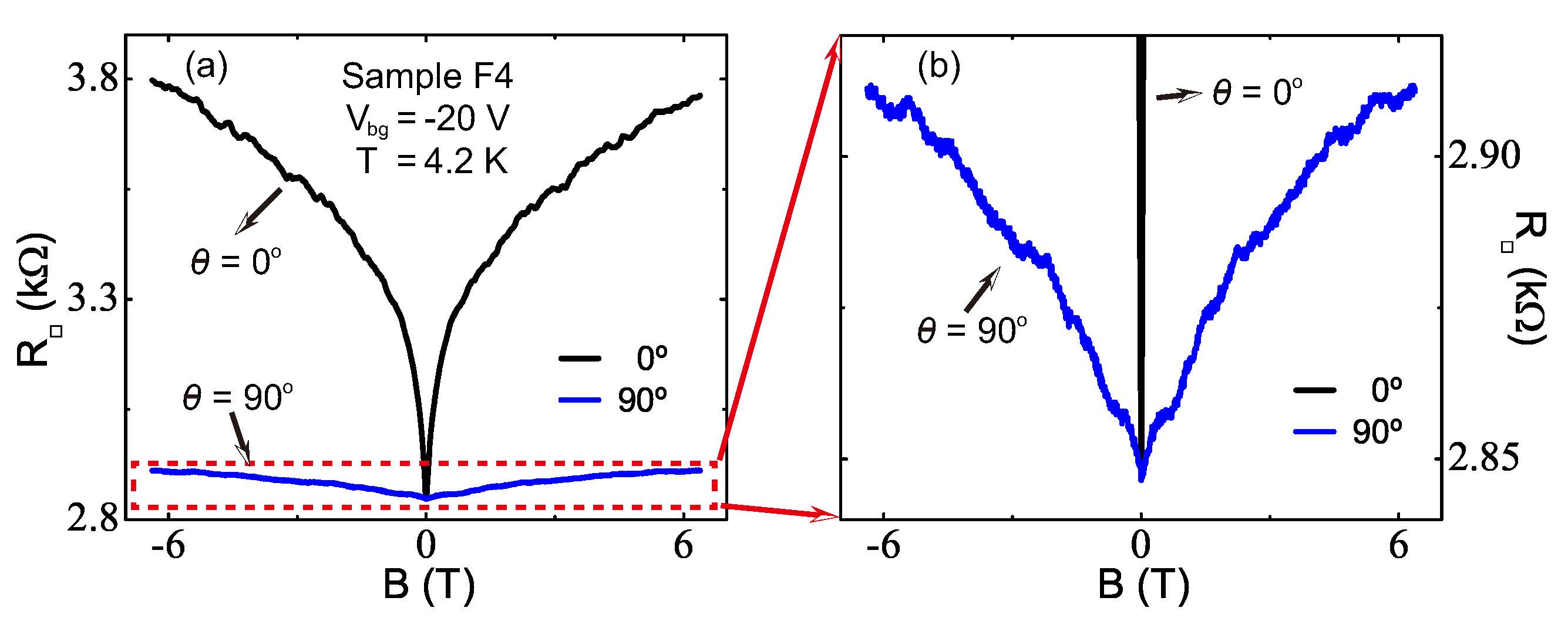
Figure 5 shows the MR at ; direction of magnetic field is in parallel with the top and bottom surfaces of the sample and perpendicular to the current direction (see Fig. 2(a) in main text). If the conduction in our thin flakes was only through the two surfaces (top and bottom) and only the localization effect affected the MR, the MR should have vanished at . As shown in Fig. 5, however, a small but finite MR exists at .
The simplest inference is that the MR at is a bulk component. In Ref. [He et al., 2011], the MR proportional to at was observed. In the data analysis, this component was subtracted from the MR obtained in other field angles. Since the samples used in Ref. [He et al., 2011] had a large carrier density, the large weight of the bulk conductance was reasonable with the classical behavior of the MR supporting that analysis.
However, in our samples, as shown in Fig. 5, we did not find a valid argument to consider the MR at as the three-dimensional (3D) bulk contribution. The -type classical MR was absent at . Instead, the MR behavior was reminiscent of the WAL effect. But, there is no consensus yet on whether the magnetoconductance (MC) correction () of bulk carriers in TIs should follow the WAL or the weak localization (WL) behavior. Lu and Shen (2011); Garate and Glazman (2012) Thus, it is not clear whether the WAL-like in our data is of bulk origin.
If the MR at corresponds to the 3D bulk contribution, in order to extract of the surface conducting channels, one has to use rather than as used in the main text. But the bulk origin of is not clear. On the other hand, the magnitude of at is sufficiently smaller than that at so that the discussion on the angle dependence of MR and the dependence of MR at in the main text is not affected even without subtracting . Therefore, we used the raw data for analysis of the gate dependence of WAL effects in Fig. 3 in main text.
It is not clear what caused this finite MR at in our TI flakes. It may have arisen from the side-wall surfaces of the thin crystal or even the in-plane MR of the surface conducting channels. There are some theoretical prediction of in-plane field-dependence MC correction for a 2D system, but not in the symplectic case. Maekawa and Fukuyama (1981); Al’tshuler and Aronov (1981) To the best of our knowledge, however, in-plane field-dependence MC correction of 2D systems in the symplectic limit has not been studied yet.
Appendix D Weak anti-localization analysis
Magnetoconductance (MC) correction of a 2D system in a symplectic limit can be expressed as Eq. (2) in the main text (HLN function). If there are two independent 2D conducting channels, the equation is expanded as follows:
| (5) |
where is the digamma function, is the electron charge, corresponds to the channel with the phase relaxation length . Hikami et al. (1980) If , Eq. (5) is simplified as follows:
| (6) |
However, if , the number of fitting parameters increases up to 4 with a larger standard error. We solved this problem by taking the following simple approximation.
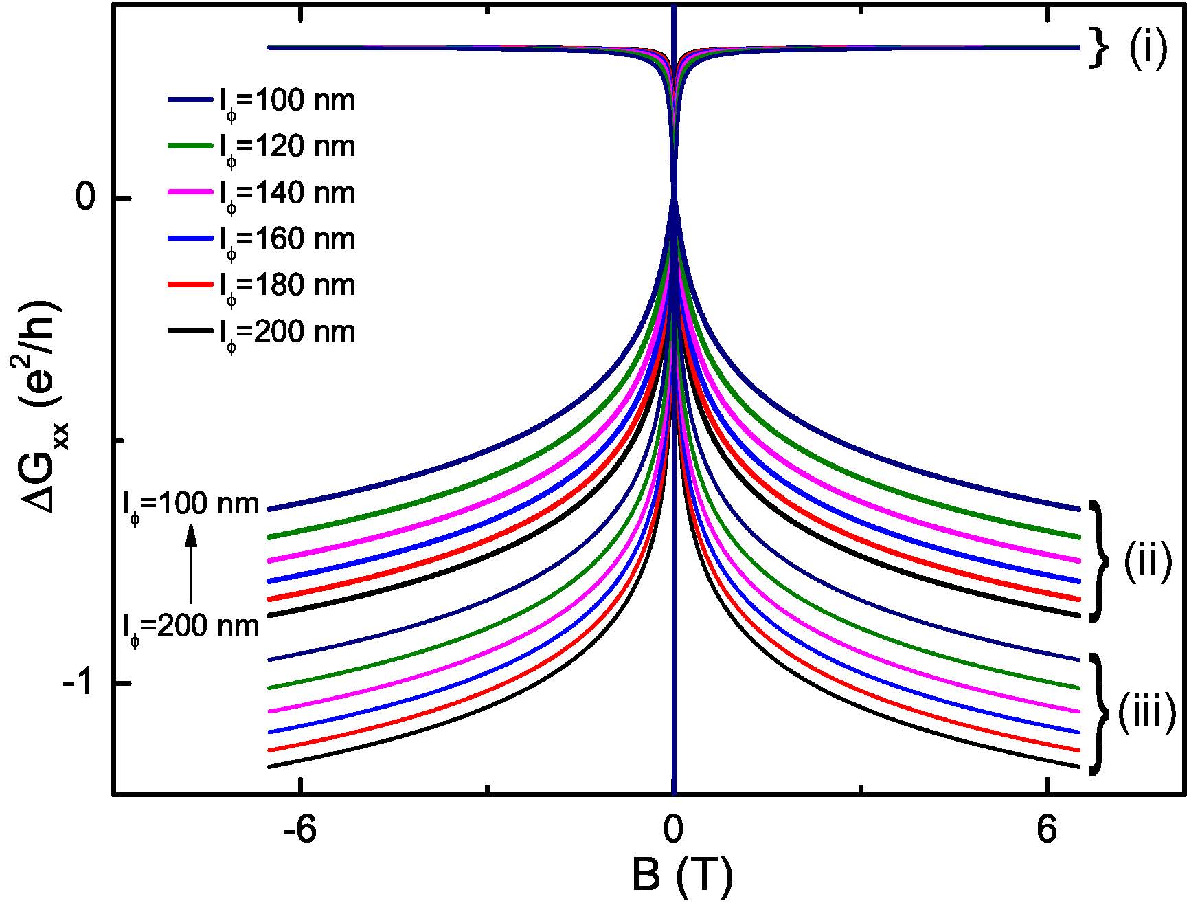
In Fig. 6, the set of curves (i) represents the digamma function part, the set (iii) corresponds to the logarithmic function part, and the set (ii) corresponds to the sum of the two parts. Each function is plotted with and nm. As displayed in Fig. 6, the digamma-function part is almost constant except in the weak-field region for different values of . Thus, the HLN expression is mostly determined by the logarithmic part. The digamma function causes a constant shift of the logarithmic function and removes the logarithmic divergence in zero field. Based on this fact, four parameters in Eq. (5) can be reduced to two parameters as follows.
Let’s define is the phase relaxation length of channel () with the corresponding coefficient and is the effective phase relaxation length with . Applying the approximated behavior of the digamma function leads to
| (7) |
The logarithmic part in Eq. (7) becomes
| (8) |
where . Therefore, with Eq. (7), the Eq. (5) can be simplified as
| (9) |
with . Figure 7 shows the validity of this approximation.
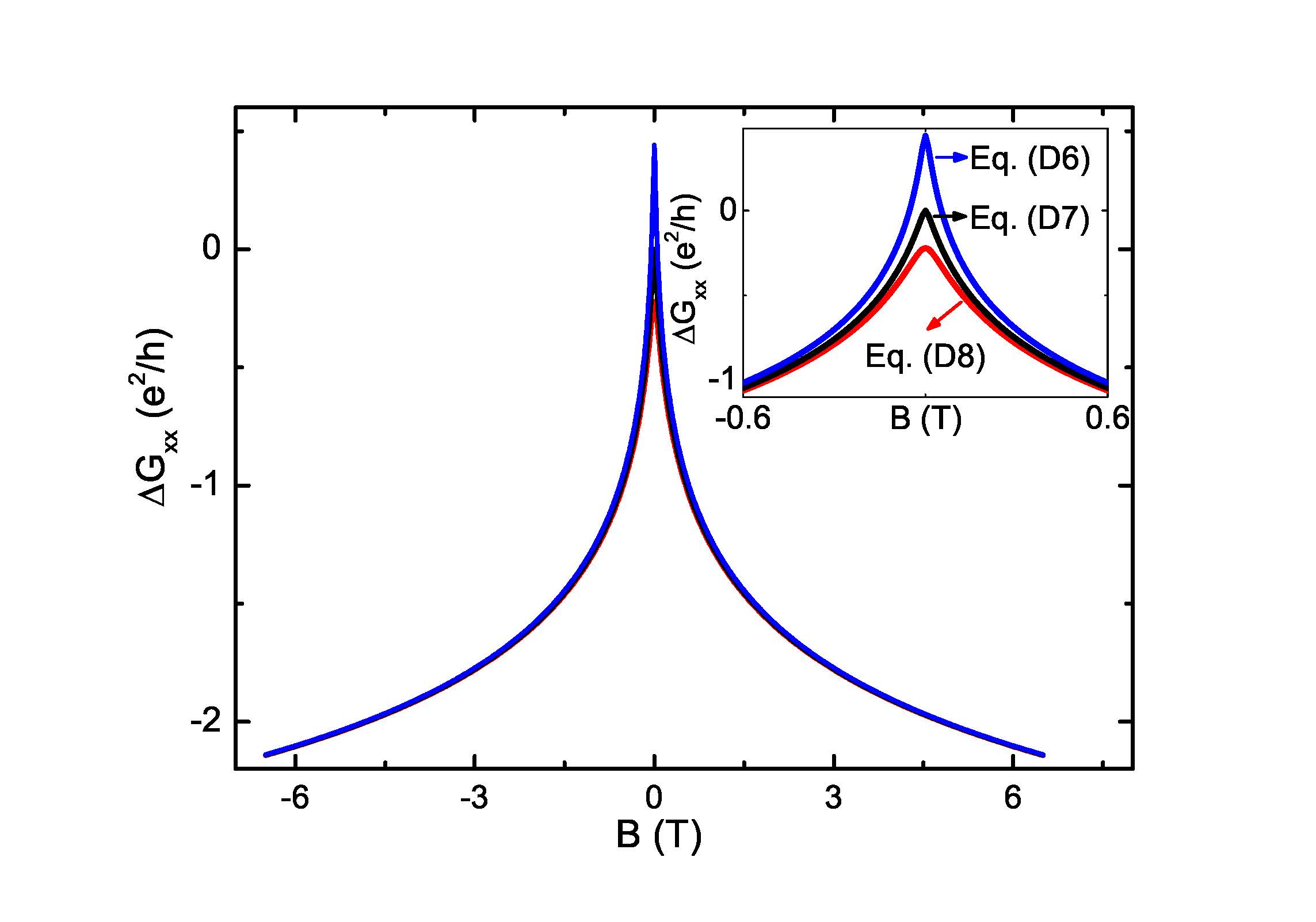
In Fig. 7, the three curves (blue, black and red online) correspond to the followings
| (10) | ||||
| (11) | ||||
| (12) |
respectively. Here, and . As displayed in Fig. 7, the deviation caused by different in digamma function can be recognized only in low fields. Furthermore, since has a value between and , the deviation may be smaller than differences displayed in Fig. 7. Therefore, even with 4 parameters in different two channels, we can apply the one-channel HLN function with two parameters and the determined and can be understood as and as Eq. (9).
Appendix E independence of the top-surface conductance
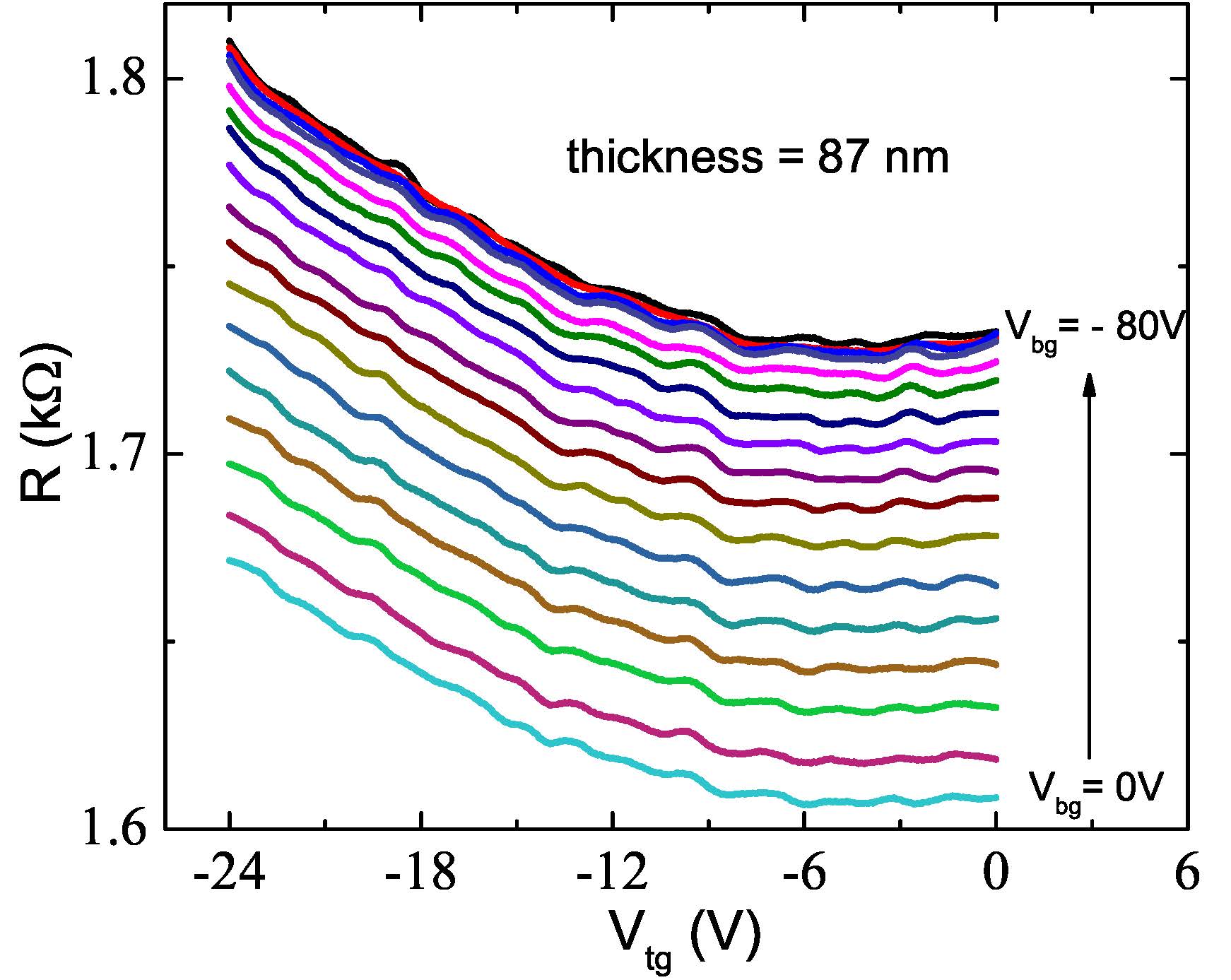
Figure 8 shows the resistance variation of an 87-nm-thick BSTS flake (thickness of this flake is almost identical to that of the samples F3 and F4) as functions of back-gate () and top-gate () voltages. This sample is not referred to in the main text. Except for the parallel shift in the resistance, the dependence of the resistance curves in Fig. 8 remains unaltered with varying . Even the positions of the resistance spikes arising from the UCF effect do not change for different values of . This feature indicates that the top-surface (bottom-surface) conductance is almost completely independent of (). Since this flake and the samples F3 and F4 are of almost identical thickness we expect that the top-surface conductance of the two samples was independent of , the fact of which is utilized in our analysis in the main text.
References
- Fu and Kane (2007) L. Fu and C. L. Kane, Phys. Rev. B 76, 045302 (2007).
- Fu et al. (2007) L. Fu, C. L. Kane, and E. J. Mele, Phys. Rev. Lett. 98, 106803 (2007).
- Zhang et al. (2009a) H. Zhang, C.-X. Liu, X.-L. Qi, X. Dai, Z. Fang, and S.-C. Zhang, Nat. Phys. 5, 438 (2009a).
- Hasan and Kane (2010) M. Z. Hasan and C. L. Kane, Rev. Mod. Phys. 82, 3045 (2010).
- Qi and Zhang (2011) X.-L. Qi and S.-C. Zhang, Rev. Mod. Phys. 83, 1057 (2011).
- Roushan et al. (2009) P. Roushan, J. Seo, C. V. Parker, Y. S. Hor, D. Hsieh, D. Qian, A. Richardella, M. Z. Hasan, R. J. Cava, and A. Yazdani, Nature 460, 1106 (2009).
- Zhang et al. (2009b) T. Zhang, P. Cheng, X. Chen, J.-F. Jia, X. Ma, K. He, L. Wang, H. Zhang, X. Dai, Z. Fang, X. Xie, and Q.-K. Xue, Phys. Rev. Lett. 103, 266803 (2009b).
- Alpichshev et al. (2010) Z. Alpichshev, J. G. Analytis, J.-H. Chu, I. R. Fisher, Y. L. Chen, Z. X. Shen, A. Fang, and A. Kapitulnik, Phys. Rev. Lett. 104, 016401 (2010).
- Xia et al. (2009) Y. Xia, D. Qian, D. Hsieh, L. Wray, A. Pal, H. Lin, A. Bansil, D. Grauer, Y. S. Hor, R. J. Cava, and M. Z. Hasan, Nat. Phys. 5, 398 (2009).
- Chen et al. (2009) Y. L. Chen, J. G. Analytis, J.-H. Chu, Z. K. Liu, S.-K. Mo, X. L. Qi, H. J. Zhang, D. H. Lu, X. Dai, Z. Fang, S. C. Zhang, I. R. Fisher, Z. Hussain, and Z.-X. Shen, Science 325, 178 (2009).
- Hsieh et al. (2009) D. Hsieh, Y. Xia, D. Qian, L. Wray, J. H. Dil, F. Meier, J. Osterwalder, L. Patthey, J. G. Checkelsky, N. P. Ong, A. V. Fedorov, H. Lin, A. Bansil, D. Grauer, Y. S. Hor, R. J. Cava, and M. Z. Hasan, Nature 460, 1101 (2009).
- Ren et al. (2011a) Z. Ren, A. A. Taskin, S. Sasaki, K. Segawa, and Y. Ando, Phys. Rev. B 84, 165311 (2011a).
- Taskin et al. (2011) A. A. Taskin, Z. Ren, S. Sasaki, K. Segawa, and Y. Ando, Phys. Rev. Lett. 107, 016801 (2011).
- Arakane et al. (2012) T. Arakane, T. Sato, S. Souma, K. Kosaka, K. Nakayama, M. Komatsu, T. Takahashi, Z. Ren, K. Segawa, and Y. Ando, Nat. Commun. 3, 636 (2012).
- Ren et al. (2012) Z. Ren, A. A. Taskin, S. Sasaki, K. Segawa, and Y. Ando, Phys. Rev. B 85, 155301 (2012).
- Chen et al. (2010) J. Chen, H. J. Qin, F. Yang, J. Liu, T. Guan, F. M. Qu, G. H. Zhang, J. R. Shi, X. C. Xie, C. L. Yang, K. H. Wu, Y. Q. Li, and L. Lu, Phys. Rev. Lett. 105, 176602 (2010).
- Checkelsky et al. (2011) J. G. Checkelsky, Y. S. Hor, R. J. Cava, and N. P. Ong, Phys. Rev. Lett. 106, 196801 (2011).
- Kim et al. (2012) D. Kim, S. Cho, N. P. Butch, P. Syers, K. Kirshenbaum, S. Adam, J. Paglione, and M. S. Fuhrer, Nat. Phys. 8, 460 (2012).
- Steinberg et al. (2010) H. Steinberg, D. R. Gardner, Y. S. Lee, and P. Jarillo-Herrero, Nano Lett. 10, 5032 (2010).
- Kong et al. (2011) D. Kong, Y. Chen, J. J. Cha, Q. Zhang, J. G. Analytis, K. Lai, Z. Liu, S. S. Hong, K. J. Koski, S.-K. Mo, Z. Hussain, I. R. Fisher, Z.-X. Shen, and Y. Cui, Nat. Nanotechnol. 6, 705 (2011).
- Hong et al. (2012) S. S. Hong, J. J. Cha, D. Kong, and Y. Cui, Nat. Commun. 3, 757 (2012).
- Wang et al. (2012) Y. Wang, F. Xiu, L. Cheng, L. He, M. Lang, J. Tang, X. Kou, X. Yu, X. Jiang, Z. Chen, J. Zou, and K. L. Wang, Nano Lett. 12, 1170 (2012).
- Analytis et al. (2010a) J. G. Analytis, J.-H. Chu, Y. Chen, F. Corredor, R. D. McDonald, Z. X. Shen, and I. R. Fisher, Phys. Rev. B 81, 205407 (2010a).
- Eto et al. (2010) K. Eto, Z. Ren, A. A. Taskin, K. Segawa, and Y. Ando, Phys. Rev. B 81, 195309 (2010).
- Analytis et al. (2010b) J. G. Analytis, R. D. McDonald, S. C. Riggs, J.-H. Chu, G. S. Boebinger, and I. R. Fisher, Nat. Phys. 6, 960 (2010b).
- Ren et al. (2010) Z. Ren, A. A. Taskin, S. Sasaki, K. Segawa, and Y. Ando, Phys. Rev. B 82, 241306 (2010).
- Petrushevsky et al. (2012) M. Petrushevsky, E. Lahoud, A. Ron, E. Maniv, I. Diamant, I. Neder, S. Wiedmann, V. K. Guduru, F. Chiappini, U. Zeitler, J. C. Maan, K. Chashka, A. Kanigel, and Y. Dagan, Phys. Rev. B 86, 045131 (2012).
- Xiong et al. (2012a) J. Xiong, A. C. Petersen, D. Qu, Y. S. Hor, R. J. Cava, and N. P. Ong, Physica E 44, 917 (2012a).
- Qu et al. (2010) D.-X. Qu, Y. S. Hor, J. Xiong, R. J. Cava, and N. P. Ong, Science 329, 821 (2010).
- Ren et al. (2011b) Z. Ren, A. A. Taskin, S. Sasaki, K. Segawa, and Y. Ando, Phys. Rev. B 84, 075316 (2011b).
- Checkelsky et al. (2009) J. G. Checkelsky, Y. S. Hor, M.-H. Liu, D.-X. Qu, R. J. Cava, and N. P. Ong, Phys. Rev. Lett. 103, 246601 (2009).
- Hikami et al. (1980) S. Hikami, A. I. Larkin, and Y. Nagaoka, Prog. Theor. Phys. 63, 707 (1980).
- Anderson (1958) P. W. Anderson, Phys. Rev. 109, 1492 (1958).
- Bergmann (1984) G. Bergmann, Phys. Rep. 107, 1 (1984).
- Xiu et al. (2011) F. Xiu, L. He, Y. Wang, L. Cheng, L.-T. Chang, M. Lang, G. Huang, X. Kou, Y. Zhou, X. Jiang, Z. Chen, J. Zou, A. Shailos, and K. L. Wang, Nat. Nanotechnol. 6, 216 (2011).
- He et al. (2012) L. He, F. Xiu, X. Yu, M. Teague, W. Jiang, Y. Fan, X. Kou, M. Lang, Y. Wang, G. Huang, N.-C. Yeh, and K. L. Wang, Nano Lett. 12, 1486 (2012).
- Cao et al. (2012) H. Cao, J. Tian, I. Miotkowski, T. Shen, J. Hu, S. Qiao, and Y. P. Chen, Phys. Rev. Lett. 108, 216803 (2012).
- Xiong et al. (2012b) J. Xiong, Y. Luo, Y. Khoo, S. Jia, R. J. Cava, and N. P. Ong, Phys. Rev. B 86, 045314 (2012b).
- Chen et al. (2011) J. Chen, X. Y. He, K. H. Wu, Z. Q. Ji, L. Lu, J. R. Shi, J. H. Smet, and Y. Q. Li, Phys. Rev. B 83, 241304 (2011).
- Kim et al. (2011a) Y. S. Kim, M. Brahlek, N. Bansal, E. Edrey, G. A. Kapilevich, K. Iida, M. Tanimura, Y. Horibe, S.-W. Cheong, and S. Oh, Phys. Rev. B 84, 073109 (2011a).
- Matsuo et al. (2012) S. Matsuo, T. Koyama, K. Shimamura, T. Arakawa, Y. Nishihara, D. Chiba, K. Kobayashi, T. Ono, C.-Z. Chang, K. He, X.-C. Ma, and Q.-K. Xue, Phys. Rev. B 85, 075440 (2012).
- Steinberg et al. (2011) H. Steinberg, J.-B. Laloë, V. Fatemi, J. S. Moodera, and P. Jarillo-Herrero, Phys. Rev. B 84, 233101 (2011).
- Zhang et al. (2011) G. Zhang, H. Qin, J. Chen, X. He, L. Lu, Y. Li, and K. Wu, Adv. Funct. Mater. 21, 2351 (2011).
- Cha et al. (2012) J. J. Cha, D. Kong, S.-S. Hong, J. G. Analytis, K. Lai, and Y. Cui, Nano Lett. 12, 1107 (2012).
- Bianchi et al. (2010) M. Bianchi, D. Guan, S. Bao, J. Mi, B. B. Iversen, P. D. C. King, and P. Hofmann, Nat. Commun. 1, 128 (2010).
- King et al. (2011) P. D. C. King, R. C. Hatch, M. Bianchi, R. Ovsyannikov, C. Lupulescu, G. Landolt, B. Slomski, J. H. Dil, D. Guan, J. L. Mi, E. D. L. Rienks, J. Fink, A. Lindblad, S. Svensson, S. Bao, G. Balakrishnan, B. B. Iversen, J. Osterwalder, W. Eberhardt, F. Baumberger, and P. Hofmann, Phys. Rev. Lett. 107, 096802 (2011).
- Benia et al. (2011) H. M. Benia, C. Lin, K. Kern, and C. R. Ast, Phys. Rev. Lett. 107, 177602 (2011).
- He et al. (2011) H.-T. He, G. Wang, T. Zhang, I.-K. Sou, G. K. L. Wong, J.-N. Wang, H.-Z. Lu, S.-Q. Shen, and F.-C. Zhang, Phys. Rev. Lett. 106, 166805 (2011).
- Choi et al. (1987) K. K. Choi, D. C. Tsui, and K. Alavi, Phys. Rev. B 36, 7751 (1987).
- Altshuler et al. (1982) B. L. Altshuler, A. G. Aronov, and D. E. Khmelnitsky, J Phys. C: Solid State Phys. 15, 7367 (1982).
- Lee and Stone (1985) P. A. Lee and A. D. Stone, Phys. Rev. Lett. 55, 1622 (1985).
- Lee et al. (1987) P. A. Lee, A. D. Stone, and H. Fukuyama, Phys. Rev. B 35, 1039 (1987).
- Garate and Glazman (2012) I. Garate and L. Glazman, Phys. Rev. B 86, 035422 (2012).
- Lu and Shen (2011) H.-Z. Lu and S.-Q. Shen, Phys. Rev. B 84, 125138 (2011).
- Gao et al. (2012) B. F. Gao, P. Gehring, M. Burghard, and K. Kern, Appl. Phys. Lett. 100, 212402 (2012).
- Cheng et al. (2010) P. Cheng, C. Song, T. Zhang, Y. Zhang, Y. Wang, J.-F. Jia, J. Wang, Y. Wang, B.-F. Zhu, X. Chen, X. Ma, K. He, L. Wang, X. Dai, Z. Fang, X. Xie, X.-L. Qi, C.-X. Liu, S.-C. Zhang, and Q.-K. Xue, Phys. Rev. Lett. 105, 076801 (2010).
- Hanaguri et al. (2010) T. Hanaguri, K. Igarashi, M. Kawamura, H. Takagi, and T. Sasagawa, Phys. Rev. B 82, 081305 (2010).
- Ashcroft and Mermin (1976) N. W. Ashcroft and N. D. Mermin, Solid State Physics (Thomson Learning, Cornell, 1976).
- Kim et al. (2011b) S. Kim, M. Ye, K. Kuroda, Y. Yamada, E. E. Krasovskii, E. V. Chulkov, K. Miyamoto, M. Nakatake, T. Okuda, Y. Ueda, K. Shimada, H. Namatame, M. Taniguchi, and A. Kimura, Phys. Rev. Lett. 107, 056803 (2011b).
- Lang et al. (2012) M. Lang, L. He, F. Xiu, X. Yu, J. Tang, Y. Wang, X. Kou, W. Jiang, A. V. Fedorov, and K. L. Wang, ACS Nano 6, 295 (2012).
- Chen et al. (2012) C. Chen, S. He, H. Weng, W. Zhang, L. Zhao, H. Liu, X. Jia, D. Mou, S. Liu, J. He, Y. Peng, Y. Feng, Z. Xie, G. Liu, X. Dong, J. Zhang, X. Wang, Q. Peng, Z. Wang, S. Zhang, F. Yang, C. Chen, Z. Xu, X. Dai, Z. Fang, and X. J. Zhou, Proc. Natl. Acad. Sci. 109, 3694 (2012).
- Ando et al. (1982) T. Ando, A. B. Fowler, and F. Stern, Rev. Mod. Phys. 54, 437 (1982).
- Fowler (1975) A. B. Fowler, Phys. Rev. Lett. 34, 15 (1975).
- Maekawa and Fukuyama (1981) S. Maekawa and H. Fukuyama, J. Phys. Soc. Jpn 50, 2516 (1981).
- Al’tshuler and Aronov (1981) B. L. Al’tshuler and A. G. Aronov, JETP Lett. 33, 499 (1981).