Intrinsic defects in silicon carbide LED as a perspective room temperature single photon source in near infrared
Abstract
Generation of single photons has been demonstrated in several systems. However, none of them satisfies all the conditions, e.g. room temperature functionality, telecom wavelength operation, high efficiency, as required for practical applications. Here, we report the fabrication of light emitting diodes (LEDs) based on intrinsic defects in silicon carbide (SiC). To fabricate our devices we used a standard semiconductor manufacturing technology in combination with high-energy electron irradiation. The room temperature electroluminescence (EL) of our LEDs reveals two strong emission bands in visible and near infrared (NIR), associated with two different intrinsic defects. As these defects can potentially be generated at a low or even single defect level, our approach can be used to realize electrically driven single photon source for quantum telecommunication and information processing.
pacs:
85.60.Jb, 61.72.jd, 78.60.FiRobust and cheap light sources emitting single photons on demand are at the heart of many demanding optical technologies Review1 ; Review2 . Single photon emission has been demonstrated in a variety of systems, including atoms SP-Atom , ions SP-Ion , molecules SP-Molecule ; SP-Molecule2 ; SP-Molecule3 , quantum dots (QDs) SP-QD ; LED-QD and color centers in diamond SP-NV ; SP-SiV . The most significant progress has been achieved for QDs QD-Cavity ; QD-Ent ; QD-BB84 , however, the necessity to use cryogenic temperatures and high inhomogeneity (the emission wavelength is individual for each QD) make this system impractical. Electrically driven single photon sources in visible have also been demonstrated using nitrogen-vacancy (NV) centers in diamond LED0-NV ; LED-NV , but the compatibility of this system with the present-day integrated circuits manufacturing is not obvious.
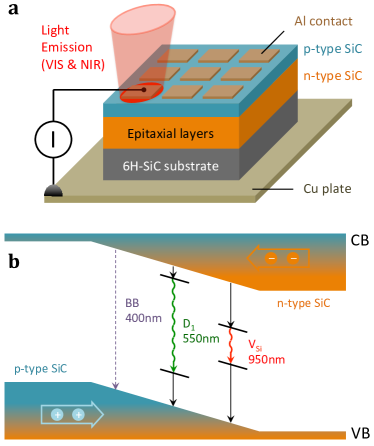
The operation principle of single photon sources is based on the quantum mechanical properties of a single two-level system. When a single photon is desired, this system is put into the excited state by an external stimulus, and a single photon is emitted upon relaxation into the ground state. A perspective approach to fabricate an efficient, room temperature single photon source based on this principle is to use color centers in semiconductors. In our work, we exploit two defect centers in SiC, the so-called defect D1-Obser and the silicon vacancy () defect SiC-SiliconVacancy , making two-color LED [Fig. 1(a)].

Remarkably, the defects in SiC comprise the technological advantages of semiconductor quantum dots and the unique quantum properties of the NV defects in diamond SiC-ResonantControl . In particular, spin qubits can be optically initialized and read out, and, therefore, our demonstration of room temperature EL from defects is an important step towards realization of all-electrical control of spins. Further, the EL reveals a broad-band emission spectrum in NIR (), where the absorption of silica glass optical fibers is relatively weak. While this spectrum range is still below the telecom window (), it can be changed in the direction of long wavelengths by proper choosing over family of -related defects in different SiC polytypes. Alternatively, the frequency conversion of NIR photons to a telecom wavelength can be applied DownConversion1 ; DownConversion2 . Therefore, the integration of defect-based SiC LEDs with existing telecommunication infrastructure seems feasible.

SiC with highly developed device technologies (e.g. MOSFETS, MEMS, sensors) is a very attractive material for practical applications. SiC is also known as the material on which the first LED has been created First-LED . Until the 90’s, SiC was used for commercial yellow and blue LEDs, but later it was replaced with GaN. The reason is that SiC is an indirect bandgap semiconductor and as a consequence direct band-to-band radiative recombination is inefficient. For the same reason, recombination through defects is preferential in SiC [Fig. 1(b)]. If one would isolate a single defect with radiative recombination channel, this property of SiC could be used to efficiently generate single photons.
The LED structures used in our experiments were grown on a n-type 6H-polytype SiC substrate [Fig. 1(a)]. First, an epitaxial 15--thick SiC layer was grown by the sublimation method. The layer is n-type with donor concentrations of (N). It also contains Ga impurities (), serving as PL activation centers. The layer is followed by a p-type SiC layer of thickness grown at a temperature of in Ar atmosphere in the presence of Al vapors (pressure ). This results in the concentration of Al acceptors of ca. . In order to generate intrinsic defects at the p-n junction the samples were irradiated with electrons to a dose of . After irradiation, the samples were annealed for 10 minutes in Ar atmosphere at a temperature of . At the final stage, Al contacts were deposited on the top of the p-type SiC layer.
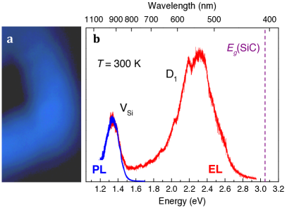
We mount LED samples on a Cu plate serving as the back electrode. Upon applying voltage between an Al contact and the Cu plate the luminescence glow is seen by the naked eye [Fig. 2(a)]. The room temperature EL spectrum of one of our LEDs is presented in Fig. 2(b). It consists of two broad emission bands, labeled as and . The corresponding recombination processes at the p-n junction are schematically shown in Fig. 1(b).
We now discuss the EL bands of Fig. 2(b) in details. Remarkably, the corresponding emission energies are significantly smaller than the bandgap of 6H-SiC (). We, therefore, ascribe them to the defects in SiC. The emission in the spectral range is characteristic for the defect D1-Obser . The nature of this defect is still not clear – several models have been proposed, including bound-exciton-like center D1-1 and first-neighbor antisite pair D1-2 . The second emission band in the NIR spectral range coincides with the photoluminescence (PL) spectrum of the silicon vacancy defects Ilyin1981 in the reference 6H-SiC bulk sample.

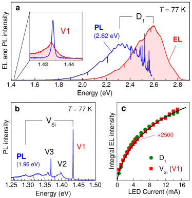
To prove this interpretation we repeat the experiment of Fig. 2(b) at a temperature of [see Fig. 3(a)], when the spectroscopic features individual for each defect can be resolved. In this low-temperature experiment, the samples are kept in vacuum and the Cu plate is also used as a cold finger. The results are summarized in Fig. 3 and below we discuss them in details.
First, we demonstrate the presence of defects in our LED structures. Figure 3(b) shows photoluminescence (PL) spectrum recorded under excitation with the energy , which is below the emission energy. Three zero-phonon lines (ZPLs) at , and are the well known fingerprint of the defects in 6H-SiC Wagber2000 . These three ZPLs originate from three nonequivalent crystallographic sites in this SiC polytype and are frequently labeled as V3, V2, and V1, respectively. The highest ZPL intensity is observed for .
Second, we demonstrate that the defect can be electrically driven. Figure 3(a) shows EL spectrum recorded at . In contrast to room temperature [Fig. 2(b)], the emission dominates in the spectrum. The reason is the much higher concentration of defects than of defects. However, the activation energy of the defect is relatively small ( D1-Donor ), leading to the intensity increase with lowering temperature. On the other hand, the activation energy of the defects is much higher and their intensity weakly depends on temperature. Indeed, we observe the characteristic ZPL at in the EL spectrum [the inset of Fig. 3(a)].
Third, we verify that the electrical excitation of the defect shown in the inset of Fig. 3(a) is not due to the re-emission process via . We excite PL with the energy of , coinciding with the maximum of the EL band [Fig. 3(a)]. The laser intensity per area is several orders of magnitude higher than that of the emission, but no significant enhancement of the PL is observed. This means that while the reemission may potentially take place, it is inefficient as compared to electrical excitation. Therefore, we conclude, the recombination of electrically injected electron and holes is responsible for the EL, as schematically shown in Fig. 1(b).
Finally, we present an input-output characteristic of one of our LED devices [Fig. 3(c)]. A clear tendency to saturation of the emission intensity with injection current is seen. This behavior can be well described as [the solid line in Fig. 3(c) corresponds to ]. The characteristic saturation current is higher than that in QD-based single photon LEDs QD-II and comparable with that in NV-based single photon LEDs LED-NV .
In conclusion, we generated intrinsic defects in SiC devices and demonstrated that these defects can be electrically driven, resulting in the efficient EL with emission energies well below the SiC bandgap. Our LEDs are two-color in a sense that they show two spectrally different emission bands associated with different defects. The defects show EL in visible, which is intense at low temperatures but quenches with rising temperature. The defects emit in NIR even at room temperature. By varying the irradiation dose one can control defect concentration, which should allow to isolate single defects, similar to single NV centers in diamond or single semiconductor QDs. Because isolated defects are ideal single photon emitters, our findings open a new way to fabricate cheap and robust LEDs emitting single photons on demand in NIR.
References
- (1) Single-photon devices and applications, C. Santori, D. Fattal, and Y. Yamamoto. (Wiley-VCH, Weinheim, 2010).
- (2) M. D. Eisaman, J. Fan, A. Migdall, and S. V. Polyakov, Rev. Sci. Instr. 82, 071101 (2011).
- (3) J. McKeever, A. Boca, A. D. Boozer, R. Miller, J. R. Buck, A. Kuzmich, and H. J. Kimble, Science 303, 1992 (2004).
- (4) M. Keller, B. Lange, K. Hayasaka, W. Lange, and H. Walther, Nature 431, 1074 (2004).
- (5) C. Brunel, B. Lounis, P. Tamarat, and M. Orrit, Phys. Rev. Lett. 83, 2722 (1999).
- (6) B. Lounis and W. E. Moerner, Nature 407, 491 (2000).
- (7) M. Nothaft, S. Höhla, F. Jelezko, N. Frühauf, J. Pflaum, and J. Wrachtrup, Nat. Commun. 3, 628 (2012).
- (8) P. Michler, A. Kiraz, C. Becher, W. V. Schoenfeld, P. M. Petroff, Lidong Zhang, E. Hu, and A. Imamoglu, Science 290, 2282 (2000).
- (9) Z. Yuan, B. E. Kardynal, R. M. Stevenson, A. J. Shields, C. J. Lobo, K. Cooper, N. S. Beattie, D. A. Ritchie, and M. Pepper, Science 295, 102 (2002).
- (10) C. Kurtsiefer, S. Mayer, P. Zarda, and H, Weinfurter, Phys. Rev. Lett. 85, 290 (2000).
- (11) E. Neu, D. Steinmetz, J. Riedrich-Möller, S. Gsell, M. Fischer, M. Schreck, and C. Becher, New J. Phys. 13, 025012 (2011).
- (12) M. Pelton, C. Santori, J. Vuc̆ković, B. Zhang, G. S. Solomon, J. Plant, and Y. Yamamoto, Phys. Rev. Lett. 89, 233602 (2002).
- (13) A. Muller, W. Fang, J. Lawall, and G. S. Solomon, Phys. Rev. Lett. 103, 217402 (2009).
- (14) T. Heindel, C. A. Kessler, M. Rau, C. Schneider, M. Fürst, F. Hargart, W.-M. Schulz, M. Eichfelder, R. Roßbach, S. Nauerth, M. Lermer, H. Weier, M. Jetter, M. Kamp, S. Reitzenstein, S. Höfling, P. Michler, H. Weinfurter, and A. Forchel, New J. Phys. 14, 083001 (2012).
- (15) A. Lohrmann, S. Pezzagna, I. Dobrinets, P. Spinicelli, V. Jacques, J.-F. Roch, J. Meijer, and A. M. Zaitsev, Appl. Phys. Lett. 99, 251106 (2011).
- (16) N. Mizuochi, T. Makino, H. Kato, D. Takeuchi, M. Ogura, H. Okushi, M. Nothaft, P. Neumann, A. Gali, F. Jelezko, J. Wrachtrup, and S. Yamasaki, Nat. Photon. 6, 299 (2012).
- (17) L. Patrick and W. J. Choyke, Phys. Rev. B 5, 3253 (1972).
- (18) P. G. Baranov, A. P. Bundakova, A. A. Soltamova, S. B. Orlinskii, I. V. Borovykh, R. Zondervan, R. Verberk, and J. Schmidt, Phys. Rev. B 83, 125203 (2011).
- (19) D. Riedel, F. Fuchs, H. Kraus, S. Väth, A. Sperlich, V. Dyakonov, A. A. Soltamova, P. G. Baranov, V. A. Ilyin, and G. V. Astakhov, Phys. Rev. Lett. 109, 226402 (2012); arXiv:1210.0505.
- (20) S. Zaske, A. Lenhard, C. A. Keßler, J. Kettler, C. Hepp, C. Arend, R. Albrecht, W.-M. Schulz, M. Jetter, P. Michler, and C. Becher, Phys. Rev. Lett. 109, 147404 (2012).
- (21) K. D. Greve, L. Y. Peter, L. McMahon, J. S. Pelc, C. M. Natarajan, N. Y. Kim, E. Abe, S. Maier, C. Schneider, M. Kamp, S. Höfling, R. H. Hadfield, A. Forchel, M. M. Fejer, and Y. Yamamoto, Nature 491, 421 (2012).
- (22) N. Zheludev, Nat. Photon. 1, 189 (2007).
- (23) A. Fissel, W. Richter, J. Furthmüller, and F. Bechstedt, Appl. Phys. Lett. 78, 2512 (2001).
- (24) A. Gali, P. Deak, E. Rauls, N. T. Son, I. G. Ivanov, F. H. C. Carlsson, E. Janzen, and W. J. Choyke, Phys. Rev. B 67, 155203 (2003).
- (25) V. S. Vainer and V. A. Ilyin, Sov. Phys. Solid State 23, 2126 (1981).
- (26) Mt. Wagner, B. Magnusson, W. M. Chen, E. Janzén, E. Sörman, C. Hallin, J. L. Lindström, Phys. Rev. B 62, 16555 (2000).
- (27) L. Storasta, F. H. C. Carlsson, S. G. Sridhara, J. P. Bergman, A. Henry, T. Egilsson, A. Hallén, and E. Janzén, Appl. Phys. Lett. 78, 46 (2001).
- (28) C. Böckler, S. Reitzenstein, C. Kistner, R. Debusmann, A. Löffler, T. Kida, S. Höfling, A. Forchel, L. Grenouillet, J. Claudon, and J. M. Gérard, Appl. Phys. Lett. 92, 091107 (2008).