Graphene single electron transistor as a spin sensor for magnetic adsorbates
Abstract
We study single electron transport through a graphene quantum dot with magnetic adsorbates. We focus on the relation between the spin order of the adsorbates and the linear conductance of the device. The electronic structure of the graphene dot with magnetic adsorbates is modeled through numerical diagonalization of a tight-binding model with an exchange potential. We consider several mechanisms by which the adsorbate magnetic state can influence transport in a single electron transistor: by tuning the addition energy, by changing the tunneling rate and, in the case of spin polarized electrodes, through magnetoresistive effects. Whereas the first mechanism is always present, the others require that the electrode has either an energy or spin dependent density of states. We find that graphene dots are optimal systems to detect the spin state of a few magnetic centers.
I Introduction
Graphene is a very promising candidate for high precision molecular sensing, due to its extremely large surface to volume ratio, and its electrically tunable large conductivity.Schedin07 ; Wernsdorfer_NL ; Pisana On the other hand, being a zero-gap semiconductor with small mass and small density of spinfull nuclei, makes graphene a material with potentially large spin lifetime both, for carriers and host magnetic dopants. Pesin2012 Taken together, these two ideas naturally lead to the use of graphene as a detector of the spin state of extrinsic magnetic centers, in the form of magnetic adatoms, vacancies and spinfull molecules. This connects with recently reported Wernsdorfer_NL ; Candini-PRB-2011 experiments in which gated graphene nanoconstrictions, operating in the single electron transport (SET) regime, showed hysteresis in the linear conductance when a magnetic field is ramped. This behavior was observed both when the molecular magnets were intentionally deposited on graphene, as well as in carbon nanotubes,Wernsdorfer_NatMat but also in the case of bare graphene nanojunctions,Candini-PRB-2011 where some type of graphene local moments Yazyev07 ; Palacios2008 ; Soriano2010 is probably playing a role.
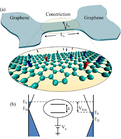
The graphene spin sensor experiments of Ref. Wernsdorfer_NL, , are performed in the Coulomb Blockade regime, showing a vanishing linear conductance except in the neighborhood of specific values of the gate voltage . This means that the graphene nanoconstriction is weakly coupled to the electrodes and has a charging energy larger than the thermal energy ( mK). The height of the linear conductance peaks is significantly smaller than , the quantum of conductance. These conditions imply that transport takes place in the sequential regime.Beenakker Thus, current flow takes place due to sequential tunneling of electrons through the graphene constriction, which we refer to as the central region in the rest of the paper, and the entire device behaves like a single electron transistor.Geim2008 ; review-dot
The aim of this work is to provide a theoretical background to understand how the magnetic state of localized magnetic moments affects transport through the graphene nanoconstriction in the SET regime. This is different from previous works where the influence of the magnetic state of magnetic edges Fede2009 and adsorbed hydrogens Soriano2010 on the conductivity was studied in the ballistic regime, with a central island strongly coupled to the electrodes, and also in the diffusive regime,Castro-Neto as well as SET through graphene islands with magnetic zigzag edges.Ezawa
The paper is organized as follows. In Sec. II we discuss a tight-binding Hamiltonian for the graphene island exchanged coupled to the spins of the magnetic adsorbates. The results of this microscopic calculation justify the use of a simple single-orbital spin-split model for the SET, discussed in section III, together with the possible mechanisms that enable the magnetic sensing. Finally, conclusions are presented in Sec. IV.
II Model for graphene island with magnetic adsorbates
II.1 Hamiltonian
Our starting point is a microscopic model for electrons confined in a graphene nanoisland which are exchanged coupled to the magnetic centers. The graphene central island is described with a tight-binding Hamiltonian for the honeycomb lattice contained in a rectangular stripe of dimensions . In order to avoid the spin-polarized states formed at the the zigzag edges,Yazyev ; JP_JR we impose periodic boundary conditions in one direction so that the structure only has open edges of armchair type. The coupling to the magnetic moments of the adsorbate molecules is then assumed to be a local exchange or spin-dependent potential, affecting sites randomly selected in the graphene central island. For simplicity, we consider that the magnetic moments of the molecules are all oriented along the same axis, which we choose as the spin quantization axis. These assumptions are good approximations in the case of strongly uniaxial TbPC2 molecules.Wernsdorfer_NL Hence, we can write the Hamiltonian of the graphene and adsorbates as
| (1) |
where is the tight-binding Hamiltonian for -electrons in graphene considering nearest neighbor interactions, is the strength of the exchange coupling between the graphene electrons and the magnetic moment of the molecules, which can take two values, . Finally, the last term in the Hamiltonian describes the electrostatic coupling of the total charge of the dot, which can be either or , given by the difference in the number of electrons and the number of carbon atoms in the central island. is the local spin density of the electrons in graphene at site ,
| (2) |
where creates an electron at the orbital of site of graphene. In the following we assume that magnetic fields controlling the spin orientation of the adsorbates, are applied along the plane of graphene so that it is a good approximation to neglect the diamagnetic coupling to the graphene electrons.
There are several independent microscopic mechanisms for spin dependent interaction between magnetic adsorbates and the graphene electrons that can be modeled with Eq. (1). In the case of magnetic molecule such as TbPC2, used in in Ref. Wernsdorfer_NL, , the magnetic Tb atom is separated from the graphene electrons by the non-magnetic atoms of the molecule, and the most likely mechanism for spin coupling is kinetic exchange.Anderson61 This coupling will generate a local Kondo-exchange between graphene electrons and the molecules.Schrieffer-Wolff More complicated scenarios, like coupling of graphene electrons to unpaired electrons in the organic rings of the molecules, would imply that every molecule affects several sites in graphene. Direct dipolar coupling would also affect several sites per molecule, but the average magnetic field created by a magnetic moment of 5 at 0.5 nm on a disk with an area around 400 nm2, the graphene constriction area in Ref. Wernsdorfer_NL, , is smaller than 1 T, which would yield a negligible maximal Zeeman coupling of neV per molecule.
II.2 Relevant energy scales
The reported dimensions of the central region, nm, lead to an energy spacing of the single particle spectrum much larger than the temperature and the charging energy.Geim2008 ; review-dot We also assume that the exchange induced shifts are smaller than the single particle splitting. As a result, the effect of exchange is to shift the bare energy levels, without mixing them. Thereby, we can safely assume that electrons tunnel through just one of the single particle levels, which might be spin-split due to exchange with molecules. We assume that the charge of the central island fluctuates between and , and that the transport level is the lowest unoccupied level of the central island spectrum. The energy of the transport level reads:
| (3) |
where is the single particle electron level, denotes the spin direction and is the magnitude of the spin splitting, which is a functional of the magnetic landscape .
Within our model, a given magnetic landscape is defined by the location and the magnetic state of the magnetic adsorbates. In Figs. 2 (a, b), we plot the value of for all the possible magnetic states of a given arrangement of atoms, for two different values of . This choice corresponds to the estimated number of molecules in Ref. Wernsdorfer_NL, . These figures show a correlation between the magnitude of the splitting and the total magnetization . The dispersion of for a fixed total magnetization is the outcome of indirect exchange couplingBrey-Das-Sarma
For comparison with the experiments, it is worth considering two extreme magnetic landscapes. At large external field, all the magnetic moments are aligned, i.e., . We refer to this as the ferromagnetic (FM) landscape. At magnetic fields smaller than the coercive field of the magnetic molecules, their average magnetization should be zero and thus, . We refer to these cases as non-magnetic (NM). In order to sample the positional disorder we perform an average over positional configurations, both for NM and FM cases. For a fixed spin choice with , an average over positional configurations yields . The reciprocal statement is also true: for a fixed positional configuration, an average over all the magnetic landscapes with also yields an average .
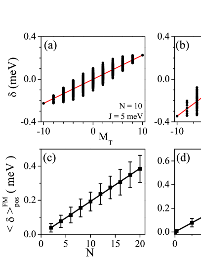
In Fig. 2 we plot the average over realizations as a function of the number of molecules [Fig. 2(c)] and as a function of the molecule electron exchange [Fig. 2(d)]. We have also calculated fixing the number of magnetic centers , the strength of the coupling and changing , the total number of carbon atoms in the island. We find that the results of all these simulations can be summarized in the following equation:
| (4) |
Whereas this result has been obtained from exact numerical diagonalization of the Hamiltonian, this dependence can be rationalized using first order perturbation theory, which yields the spin dependent shift of the transport level:
| (5) |
where is the wave function of the transport orbital. We now use so that we can approximate:
| (6) |
Using the fact that for the FM configurations and for the NM ones, we arrive to Eq. (4).
III Spin-Split Single Orbital Model for SET
In this section we discuss SET across a central island with a single spin split particle level. This is justified by the results of the previous section. We obtain expressions for the current of the system and we discuss the conditions under which the conductance depends on the magnetic state of the single electron transport.
III.1 Single electron transistor with a spin-split single orbital model
We consider single electron transport though a spin split single transport level,Recher2000 with energy . We assume that the occupation of the transport level can be either 0 or 1, the doubly occupied configuration being much higher in energy. Within these approximations, the transport level has three relevant many body states: uncharged, and the two charged with or spins. In the zero-applied bias limit, each of these states will be occupied according to the thermal equilibrium distribution, which we denoted as , and respectively. In the SET regime we are interested and within the linear response (), transport will be enabled only when the addition energy lies within the thermally broadened transport window defined by the applied bias.
Under these approximations, the current flowing from the left electrode to the central island is given by:
| (7) |
where and are rates for electron tunneling from the left electrode to the dot and vice-versa. Continuity equation ensures that this current is identical to the current flowing towards the right electrode and, thereby, equal to the net current flow. The tunneling rates for electron tunneling out of and into the dot Haug_Jauho_book_1996 are given respectively by
| (8) |
and
| (9) |
where is the strength of the dot - left electrode coupling, and
| (10) |
are the spin dependent addition energies. Importantly, both and appear on equal footing, as additive quantities in this equation. The density of states of the left electrode, evaluated at the spin-dependent transport level energy, is denoted by , while denotes the Fermi function. The electrode Fermi energy is taken to change linearly with the bias voltage . In the zero bias limit, the linear conductance reads:
| (11) |
where
| (12) |
is the single particle tunneling rate between the electrode and the transport level.
III.2 Influence of magnetic state on conductance
From the above discussion it is apparent that, for a given gate potential and temperature , the linear conductance depends on the magnetic landscape affecting the central island through two classes of independent mechanisms, illustrated in Fig. 3:
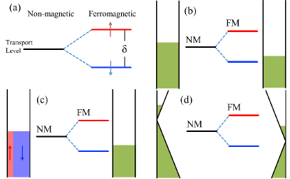
In the first mechanism the change in the magnetic state modifies the value of , which must have a similar effect than changing the gate potential. It resembles the magneto-Coulomb effect,Ono ; Vanwees by which the applied magnetic field changes the Fermi energy of the electrode, shifting the curves. However, this first mechanism necessarily implies a change of sign of the variation of as the gate potential is scanned along the resonance (see top panel of Fig. 4). Importantly, this is not observed in the experiments with magnetic molecules,Wernsdorfer_NL but it is observed in the case of graphene nanoconstrictions.Candini-PRB-2011
Motivated by the behavior reported in Ref. Wernsdorfer_NL, , we pay attention also to the second mechanism. For spin un-polarized transport, the change in the transport energy level results in a change on tunneling rate only if the electrode density of states depends on energy, which is exactly the case of graphene. For spin-polarized transport, the relative orientation of the electrode and island magnetic moment give rise to magneto-resistive effects that are accounted for by the changes in
III.3 Transport for constant tunneling rates
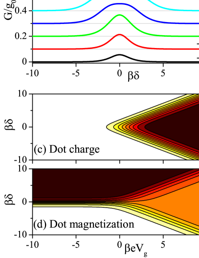
We now discuss our transport simulations for the graphene single electron transistor spin sensor. We focus on the first spin sensing mechanism in a single electron transistor: changes in spin splitting of the transport level produce changes in addition energies (figure (3)b). For that matter, we neglect both the energy and spin dependence of the tunneling rates . In Fig. 4(a) we show the linear conductance, in units of , as a function of gate voltage, for several values of the transport level splitting , in units of . It is apparent that the Coulomb Blockade peaks undergoes a lateral shift, as expected from the fact that and appear on equal footing on the spin dependent addition energies. At the two spin channels contribute. Therefore, as we increase , the height of the conductance peaks decreases, because one of the two spin channels is removed from the transport window of width
In figure (4)b we plot the variations in the linear conductances as a function of the spin splitting , for several values of . We see two types of curves. For values of such that the transport level is occupied, as we increase the transport level is pushed downwards, away from the elastic transport window, switching off the transistor conductance. In contrast, for such that the transport level is empty for , lying above the elastic transport window, ramping makes one of the two spin states of the transport level enter the transport window, giving rise to the double peak structure. The fact that and play analogous roles is illustrated in Figs. 4(c, d), where we show the average magnetization and occupation of the transport level in the phase diagram defined by these two variables.
III.4 Transport with energy dependent tunneling rates
We now consider the second mechanism for spin sensing in a single electron transistor: changes in spin splitting of the transport level produce changes in the tunneling rates . This can happen for two reasons:
-
1.
One of the electrodes is spin polarized, so that . Spin polarized transport is sensitive to the product of the magnetic moment of electrode and central island. This type of effect has been thoroughly discussed in the case of SET with ferromagnetic electrodes.Barnas98 ; Seneor2007
-
2.
The density of states of the electrode depends on energy. Thus, changes in the transport level change , for both spins. This is a natural scenario for graphene electrodes. dots_Ensslin ; Sols-Guinea
Let us consider first the case of spin polarized electrodes. We do the assumption that the density of states are spin dependent but energy independent: , with the electrode polarization. In Fig. 5(a) we plot the linear conductance vs curves for several values of the splitting , assuming a large value of the electrode spin polarization . It is apparent that, on top of the shift of the resonance curve whose origin was discussed in the previous subsection, there is a change in the amplitude of the curve. Notice that and are smaller than for all values of . In this specific sense, the gate-independent spin contrast is similar to the experimental report with magnetic molecules.Wernsdorfer_NL In Fig. 5(a) we show the linear conductance as a function of for different values of . It is apparent that, as opposed to the case of non-magnetic electrodes shown in Fig. 5(b), the function ) is no longer an even functions, reflecting the magneto-resistive behaviour. Basically, transport is favored when the spin polarization of the electrode and the central island are parallel.
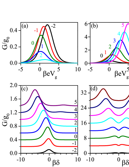
We now consider a non-spin polarized electrode with an energy dependent density of states. This scenario occurs naturally in graphene. If we consider idealized graphene electrodes, neglecting effects of interactions, disorder and confinement, we have , where is the Dirac point. The curves, shown in Fig. 5(b) for different values of , shift and change amplitude. The shift is related to the change of the addition energies, discussed in the previous subsection, and the change in amplitude comes from the variation of the tunneling rate as the transport level scans the energy dependent density of states of the electrode.
In Fig. 5(d) we plot for several values of . The curves are similar to the case with energy independent tunneling rates, except for the dip at zero which occurs because we chose the bare transport level right at Dirac point. This is the most favorable choice to maximize the effect of energy dependence of . From our results, and given the fact that experimentally is not possible to put the Fermi energy arbitrarily close to the Diract point,Geim-closest we find it unlikely that this effect is playing a role in the experiments.
III.5 Sensitivity of the single electron transistor spin sensor
We now discuss the sensitivity of the spin sensor based on the graphene single electron transistor, as described by our model, neglecting changes in . From Fig. 4(a) we propose, as rule of thumb, that variations of similar or larger than can be resolved. Estimating from the case of fully spin polarized magnetic adsorbates, given in Eq. (4), we find a relation between the minimal number of magnetic centers that can be detected, and the temperature and exchange constant:
| (13) |
It is apparent that decreasing the temperature, or increasing the spin-graphene exchange coupling, increases the sensitivity of the device (makes it possible to detect a smaller concentration of molecules). For instance, at mK, and taking , which corresponds to an approximate area of nm2, one could detect molecules for an exchange coupling meV.
Recent reports have shown that it is possible to fabricate graphene nano islands with lateral dimensions of 1nm.Barreiro2012 These dots have . Thus, they would permit the detection of the spin of a single magnetic adsorbate provided that is kept hundred times smaller than . For mK this implies meV. Interestingly, in such a small dot Coulomb Blockade persists even at room temperature, but increasing keeping the sensitivity would require also to increase .
IV Discussion and conclusions
Because of its structural and electronic properties, graphene is optimal for a spin sensor device. Being all surface, the influence of adsorbates on transport should be larger than any other bulk material. Because of the linear relation momentum and large Fermi velocity, energy level spacing in graphene nano structures can easily be larger than the temperature, the tunneling induced broadening, and the perturbations created by the adsorbates. One of the consequences is that single electron transport takes place through a single orbital level.
Our simulations show how the spin splitting of the transport level is sensitive to the average magnetization of the magnetic adsorbates, which is controlled by application of a magnetic field along the plane of graphene, to avoid diamagnetic shifts. On the other hand, the linear conductance of the single electron transistor depends on , which accounts for the sensing mechanism. More specifically, depends on due to either changes in the spin dependent addition energies or changes in the electrons lifetime . The first is independent of the nature of the electrodes, whereas the second only happens if they are magnetic or have an energy dependent density of states.
We have shown how, within an independent particle model and in the single electron transport regime, the energy dependence of the graphene electrode density of states can only be relevant if the transport energy level is fine tuned to the Dirac point. However, this fine tuning is quite unlike to happen in experimental conditionsGeim-closest . Still, the combined action of disorder and Coulomb interaction could give rise to a so called Coulomb Gap in the density of states of graphene, that might make the tunneling rates depend on the energy.Coulomb-gap-graphene ; Coulomb-gap-graphene1 ; Coulomb-gap-graphene2
Finally, we have assumed that both the edges of the graphene island and graphene electrodes are non-magnetic. Our discussion of the effect of spin-polarized electrodes on the transport properties of the device would be valid for electrodes with ferromagnetic zigzag edges. A second possibility, out of the scope of this work, is to consider a graphene single electron transistor whose central island has ferromagnetic edges. This case has been already studied. Ezawa
In conclusion, we have studied the mechanisms by which a graphene single electron transistor could work as a sensor of the magnetic order of magnetic atoms or molecules adsorbed on the graphene central region. Our work has been motivated in part by recent experimental works, Wernsdorfer_NL ; Candini-PRB-2011 . Whereas further work is still necessary to nail down the physical mechanisms for the spin sensing principles underlying the experimental work, our study provides a conceptual framework for graphene single electron transistor spin sensors.
This work has been financially supported by MEC-Spain (Grant Nos. FIS2010-21883-C02-01 and CONSOLIDER CSD2007-0010) as well as Generalitat Valenciana, grant Prometeo 2012-11. We thank A. Candini for useful comments on the manuscript.
References
- (1) F. Schedin, A. Geim, S. Morozov, E. Hill, P. Blake, M. Katsnelson, and K. Novoselov, Nature Materials 6, 652 (2007).
- (2) A. Candini, S. Klyatskaya, M. Ruben, W. Wernsdorfer, and M. Affronte, Nano Letters 11, 2634 (2011).
- (3) S. Pisana , P. M. Braganca , E. E. Marinero and B. A. Gurney, Nano Letters 10, 341 (2010).
- (4) D. Pesin and A. MacDonald, Nature Materials 11, 409(2012).
- (5) A. Candini, C. Alvino, W. Wernsdorfer, M. Affronte, Physical Review B 83, 121401 (2011).
- (6) M. Urdampilleta, S. Klyatskaya, J. Cleuziou, M. Ruben, and W. Wernsdorfer, Nature Materials 10, 502 (2011).
- (7) O. V. Yazyev and L. Helm, Physical Review B 75, 125408 (2007).
- (8) J. J. Palacios, J. Fernández-Rossier, L. Brey, Physical Review B 77, 195428 (2008).
- (9) D. Soriano, F. Muñoz-Rojas, J. Fernández-Rossier, J. J. Palacios, Physical Review B 81, 165409 (2010).
- (10) C.W.J. Beenakker, Physical Review B 44, 1646 (1991).
- (11) L. Ponomarenko, F. Schedin, M. Katsnelson, R. Yang, E. Hill, K. Novoselov and A. K. Geim, Science 320, 356 (2008).
- (12) J. Güttinger, F. Molitor, C. Stampfer, S. Schnez, A. Jacobsen, S. Dröscher, T. Ihn and K. Ensslin, Rep. Prog. Phys. 75, 126502 (2012).
- (13) F. Muñoz-Rojas, J. Fernández-Rossier, J. J. Palacios, Physical Review Letters 102, 136810 (2009).
- (14) C. H. Lewenkopf, E. R. Mucciolo, and A. H. Castro Neto, Physical Review B 77, 081410(R) (2008).
- (15) M. Ezawa, Physical Review B 77, 155411 (2008).
- (16) J. Fernández-Rossier and J. J. Palacios, Phys. Rev. Lett. 99, 177204 (2007).
- (17) O. V. Yazyev, Rep. Prog. Phys. 73, 056501 (2010).
- (18) L. Brey, H. A. Fertig, and S. Das Sarma, Phys. Rev. Lett.99, 116802 (2007).
- (19) P. W. Anderson Phys. Rev. 124, 41 (1961).
- (20) J. R. Schrieffer and P. A. Wolff Phys. Rev. 149, 491 (1966).
- (21) P. Recher, E. V. Sukhorukov, and Daniel Loss Phys. Rev. Lett. 85, 1962 (2000).
- (22) H. Haug and A.-P. Jauho, Quantum kinetics in transport and optics of semi-conductors (Springer-Verlag, Berlin, 1996).
- (23) K. Ono, H. Shimada, and Y. Ootuka, Journal of the Physical society of Japan 66, 1261 (1997).
- (24) S. J. Van Der Molen, N. Tombros, and B. J. Van Wees, Physical Review B 73, 220406 (2006).
- (25) J. Barnas, A. Fert Phys. Rev. Lett. 80 1058 (1998).
- (26) P. Seneor, A. Bernand-Mantel and F. Petroff, Journal of Physics: Condensed Matter 19, 165222 (2007).
- (27) A. Barreiro, H.S.J. van der Zant, L.M.K. Vandersypen, Nano Letters 12, 6096 (2012).
- (28) A. Mayorov, D. C. Elias, I. S. Mukhin, S. V. Morozov, L. Ponomarenko, K. S. Novoselov, A. K. Geim, and R. V. Gorbachev, Nano Letters 12, 4629 (2012).
- (29) S. Dröscher, H. Knowles, Y. Meir, K. Ensslin, and T. Ihn, Physical Review B 84, 073405 (2011).
- (30) A. L. Efros, and B. I. Shklovskii, J. Phys. C: Solid State Phys. 8 49 (1971).
- (31) B. Terrés, J. Dauber, C. Volk, S. Trellenkamp, U. Wichmann, and C. Stampfer, Applied Physics Letters 98, 032109 (2011).
- (32) X. Liu, J. B. Oostinga, A. F. Morpurgo, and L. M. K. Vandersypen, Physical Review B 80, 121407(R) (2009).
- (33) F. Sols, F. Guinea, and A. H. Castro Neto, Physical Review Letters 99, 166803 (2007).