Electronic Structure and Quasiparticle Band Gap of Silicene Structures
Abstract
We report first-principles results on the electronic structure of various silicene structures. For planar and simply buckled silicenes, we confirm their zero-gap nature and show a significant renormalization of their Fermi velocity by including many-electron effects. However, the other two recently proposed silicene structures exhibit a finite band gap, indicating that they are gapped semiconductors instead of previously expected Dirac-fermion semimetals. Moreover, our calculated quasiparticle gap quantitatively explains the recent angle-resolved photoemission spectroscopy measurements. In particular, the band gap of the latter two structures can be tuned in a wide range by applying strain, giving hope to bipolar-devices applications.
Graphene, a layer of hexagonal carbon lattices, has spurred tremendous interest because of its unique linear energy-momentum dispersion and exciting applications. 2004Novoselov ; 2005Novoselov ; 2005Zhang ; 2006Berger ; 2009Castro Its huge success has also motivated significant efforts to look for the similar honeycomb structures but made of other group IV elements, such as silicon and germanium, which are so called silicene and germanene,1994Takeda ; 2007Voon ; 2009Cahangirov ; 2010Aufray ; 2010Padova ; 2010Lalmi ; 2010Houssa ; 2011Liu ; 2012Vogt ; 2012Fleurence ; 2012Chen ; 2012Lin respectively. Particularly because of the compatibility with the matured silicon technologies and the stronger spin-orbit coupling for potential topological insulator candidates, 2011Liu silicene is expected to be a promising material both theoretically and practically.
Because of the strong trend of electrons of silicon atoms to form the tetrahedral hybridization, unlike graphene, a simply buckled silicene structure is predicted to be more stable than the perfectly planar one.2009Cahangirov This buckling provides a unique degree of freedom to silicene atomistic structures; to date several unique structures with more complicated buckling styles are proposed by recent experiments, in which a layer of silicene has been successfully fabricated on metallic substrates.2012Vogt ; 2012Fleurence ; 2012Chen ; 2012Lin The Dirac-fermion energy-momentum dispersion is observed in these silicene structures as well.2012Vogt ; 2012Fleurence ; 2012Chen ; 2012Lin ; 2012Feng However, other than interpreting atomistic structures, very limited attempts have been carried out to discover the electronic structures of these recently proposed silicene structures, which is crucial for guiding experimental measurements and understanding the electric and optical properties of these materials of ever-growing interest.
Moreover, the buckling of silicon atoms may break the symmetry of the honeycomb lattice. According to the history of graphene, the variation of structure and symmetry shall not only change the Fermi velocity but also possibly generate a finite band gap, promising a crucial advantage over graphene for broader applications, such as bipolar devices and high-performance field-effect transistors (FETs).
In this Letter, we present our first-principles calculations, using both density functional theory (DFT) and many-body perturbation theory (MBPT), to reveal the electronic structures of several promising silicene structures. Our study shows that both the planar and simply buckled silicene structures have a gapless linear energy-momentum dispersion and that the self-energy correction contributes to a significant enhancement of the Fermi velocity (). However, for the two recently proposed silicene structures, a finite band gap is identified and this gap value can even be varied in a wide range by tuning the strain. The inclusion of many-electron effects by the GW approximation further confirms this finite band gap, which corrects the previous key interpretation of these silicene structures as massless Dirac-fermion semimetal. At the same time, our GW calculated band gap satisfactorily explains the recent angle-resolved photoemission spectroscopy (ARPES) measurements. On the other hand, the tunable band gap of silicene according to the applied strain predicts promising device applications, overcoming the known trouble of gapless graphene.
For our DFT simulations, both local density approximation (LDA) and generalized-gradient approximation (GGA) are applied to make sure our conclusions are not sensitive to the choice of functionals. 1964Hohenberg ; 1965Kohn The Kohn-Sham equation is solved using the plane-wave basis with a 24 energy cutoff. Norm-conserving pseudopotentials 1991Troullier are applied and the k-point sampling grid is set to be dense enough to obtain converged DFT eigenvalues. In order to provide more quantitative results with many-electron effects included, the single-shot approximation is employed to calculate QP band gaps 1986Hybertsen ; 2012Deslippe with a layered Coulomb truncation. The k-grid sampling of such GW calculations is for planar and simply buckled silicene structures while and for those proposed by recent experiments, respectively.
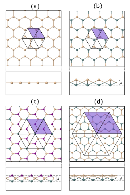
Here we consider four typical silicene structures of current fabrication interest, which are shown in Fig. 1. The first two are known planar and simply buckled structures while the last two are proposed by recent experiments with () and () structures, respectively. 2012Vogt ; 2012Chen The main differences between these structures are the size of the unit cell and the way to buckle the lattices. For example, the silicon atoms in the () structure shown in Fig. 1 (c) are located in three horizontal planes while those in the () structure shown in Fig. 1 (d) are located in two horizontal planes. According to the total energy of DFT, the simply buckled structure shown in Fig. 1 (b) is the most stable configuration with the in-plane lattice constant of 3.81 Å and a buckling distance 0.40 Å, which are in agreement with previous results. 2009Cahangirov ; 2011Liu ; 2012Vogt
It has to be pointed out that those structures shown in Figs. 1 (c) and (d) do not exactly mimic the experimental cases, in which the substrate may be an essential ingredient 2012Vogt ; 2012Chen . This is indicated by our DFT calculations, and other published works show that these isolated structures are only metastable. 2012Chen Therefore, as what have been done before,2012OHare our solution is to fix the buckling distance and relax all other degrees of freedom, including force and stress. Our following calculations will show that the essential physical picture and main conclusions shall not be affected by this approximation.
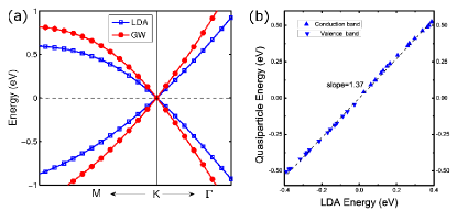
For the planar and simply buckled silicene structures shown in Figs. 1 (a) and (b), both DFT and GW calculations confirm the zero-gap nature with a linear massless Dirac-fermion dispersion. Since planar silicene has nearly the same energy-momentum dispersion (with slightly different Fermi velocities) and GW-LDA correction as the simply buckled silicene, we only provide the results of the simply buckled case in Fig. Fig. 2. Figure 2 (a) shows the band structures around the Dirac Cone for the simply buckled silicene, and Fig. 2 (b) shows its quasiparticle energy vs. LDA band energy relation. A perfect linear relation is observed, which means the zero-gap linear band dispersion is kept even including many-electron effects. From these linear energy-momentum dispersions, we get the corresponding Fermi velocity of the planar silicene as 5.6 m/s and that of simple buckled structure as 5.4 m/s at the DFT level. After including the electronic self-energy corrections by the GW approximation, these values are enhanced to be 7.7 m/s and 7.4 m/s, respectively. These Fermi velocities are substantially smaller than that of graphene ( 1.1 m/s) but the renormalization of the Fermi velocity by self-energy corrections is similar to that of graphene, which is around a enhancement from their DFT result 2008Trevisanutto ; 2009li because of the depressed screening effect.
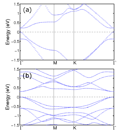
Then we turn to the recently proposed structures from experiments. In Fig. 3 (a), the DFT-calculated band structure of the buckled () structure is obtained by using the buckling distance 0.71 Å. which is a typical buckling value.2009Cahangirov ; 2012Vogt ; 2012Fleurence ; 2012Lin Surprisingly, there appears to be a finite band gap ( 0.21 eV) at the point, which is qualitatively different from previously claimed massless Dirac-fermion dispersion. 2012Chen Actually, we can obtain a well-defined effective mass of the free carriers from the curvature of the band dispersion in Fig. 3 (a). For example, the nearly isotropic effective mass of the light electron is 0.083 and that of the hole is 0.079 , which are typical values of semiconductors.
Moreover, we further tune the buckling distance while maintaining the supercell geometry to obtain the evolution of the band gap, which is presented in Fig. 4 (a). From another point of view, this is equivalent to tune the strain condition of the layer structure. For both LDA and GGA results, the band gap of such a () structure increases while enlarging the buckling distance. In particular, as the buckling distance is more than 0.8 Å, we see a transition of the band gap from the direct one to the indirect one, which is reasonable because the band structure shall approach that of tetrahedral silicon due to the stronger hybridization. Therefore, unlike the planar and simply buckled silicene, whose band gaps are always zero under uniaxial or biaxial strain, the band gap of this () silicene structure can be tuned from zero to a wide range by the mechanical strain, which shall be of broad interests.
To further confirm this finite band-gap nature, we have performed the GW calculation. For the purpose of justification, one GW calculation of a typical buckling distance shall be enough; as shown in Fig. 4 (a), the QP band gap is around 0.5 eV for the 0.71 Å buckled case, which is almost a 140 enhancement from the DFT result because of the substantially depressed screening. It must be addressed again that our referenced experiments use a metallic substrate, which may reduce the self-energy correction due to the metallic screening and possible charge transfer. However, all of these factors will not close the finite band gap and, usually, the realistic QP band gap shall still be slightly larger than the DFT result.2006neaton ; 2011li
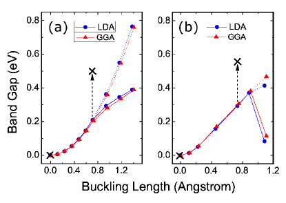
We now turn to the band structure of the other important silicene structure (), as shown in Fig. 3 (b). For this superstructure, the buckling distance 0.75 Å is chosen from the experimental study. 2012Vogt This time we observe a finite band gap again, which is a typical direct-band-gap semiconductor as shown in Fig. 3 (b). The evolution of the band gap with the buckling distance d is also presented in Fig. 4 (b). Similar to the () case, the band gap increases as we enlarge the buckling distance. When the buckling distance is more than 0.8 Å, the similar direct-to-indirect band gap transition is observed in Fig. 4 (b). The corresponding GW results are marked as well, predicting a larger QP band gap than the DFT results.
Interestingly, when we consult the relevant experimental result, a finite band gap was observed, but it had been attributed to extrinsic factors, such as the layer-substrate interaction. 2012Vogt However, our simulation shows that this finite band gap may be intrinsic if the silicene sample possesses the claimed () structure. Moreover, if we compare the experimentally observed band gap value by ARPES to our first-principles GW result shown in Fig. 4 (b), they are very close to each other, 0.56 eV from our calculation while 0.6 eV from experimental work, for the () structure with a buckling distance of 0.75 Å. 2012Vogt
After presenting first-principles results, it is necessary to figure out the physical reason for such a finite band gap opening in these promising silicene structures. According to past intensive studies on graphene, a necessary condition for the massless Dirac cone with a zero-gap character is the inversion symmetry of AB sublattices. However, for the structures shown in Figs. 1 (c) and (d), A and B sublattices are no longer equivalent to each other, resulting in the broken inversion symmetry and, thereafter, generating a finite band gap. A similar idea was noticed before, e.g., the applied gate electric field can break this symmetry and introduced a finite band gap in simply buckled silicene and germanene. 2012Ni ; 2012OHare ; 2012falko .
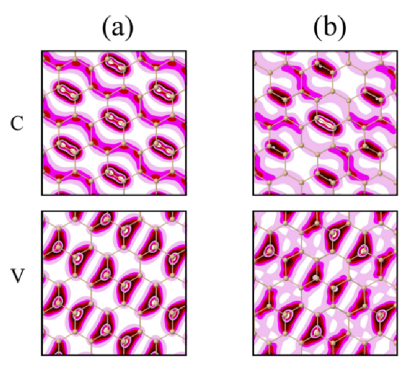
In order to better see this broken AB sublattice symmetry, we present the charge distributions of valence and conduction states at energy extrema around the band gap. As shown in Fig. 5 (a), for planar silicene, we observe the charge distributions of both valence and conduction states are nearly identical for A and B sublattices. However, for the () silicene structure, we can clearly see the inequivalent charge distribution of A and B sublattices as shown in Fig. 5 (b) due to the broken symmetry.
All the above calculations consider only free-standing silicene structures. However, the predicted finite band-gaps in the structures, as shown in Figs. 1 (c) and (d), will persist even if the substrate effect is included because the layer-substrate interactions shall further break the symmetry and enlarge the band gap. 2007Zhou In this sense, we believe that the recently proposed silicene structures have qualitatively different electronic structures and band gaps from the widely assumed massless Dirac-fermion dispersion. The most likely reason for this conflict between our simulation results and previous experimental conclusions may be due to the interpretations of atomic structures from their experimental data.
Finally we have to point out that the finite-gap nature of these recently proposed silicene structures shall be of practical interest. As shown in Figs. 3 and 4, the band gap and even the band topology can be tuned in a wide range by the buckling distance and the associated strain; this provides a precious degree of freedom to control the electronic and optical properties of such materials, making them superior to gapless graphene. According to previous studies, 2009Cahangirov ; 2010Lalmi ; 2012Vogt ; 2012Fleurence ; 2012Lin the lattice structure and buckling distance are able to be varied by layer-substrate interactions. Therefore, if future experiments can fabricate and confirm more similar structures, they shall be of broad interest for devices applications with such a tunable band gap.
In conclusion, we employ first-principles simulations to study the electronic structure of various silicenes. Our results show that the band structure of silicene is sensitive to the buckled atomistic structure. Unlike the planar and simply buckled ones, these silicene structures proposed by recent experiments exhibit a finite band gap, making them promising 2D semiconductors instead of zero-gap semimetals, as were previously assumed. On the other hand, this finite band gap can be tuned in a wide range by strains and makes these silicene structures superior to graphene for many important applications. Our predictions reinterpret relevant experimental measurements and shall motivate more reliable justifications.
We thank Ryan Soklaski for proofreading. S.H. and L.Y. acknowledge the support by NSF Grant No. DMR-1207141 and the International Center for Advanced Renewable Energy and Sustainability (I-CARES) of the Washington University. The computational resources have been provided by Lonestar of Teragrid at the Texas Advanced Computing Center and Hoppers of the National Energy Research Scientific Computing Center (NERSC). The ground state calculation is performed by the Quantum Espresso2009Giannozzi . The GW calculation is done with the BerkeleyGW package2012Deslippe .
References
- (1) K. S. Novoselov, A. K. Geim, S. V. Morozov, D. Jiang, Y. Zhang, S. V. Dubonos, I. V. Grigorieva, and A. A. Firsov, Science 306, 666 (2004).
- (2) K. S. Novoselov, A. K. Geim, S. V. Morozov, D. Jiang, M. I. Katsnelson, I. V. Grigorieva, S. V. Dubonos, and A. A. Firsov, Nature (London) 438, 197 (2005).
- (3) Y. Zhang, Y.-W. Tan, H. L. Stormer, and P. Kim, Nature (London) 438, 201 (2005).
- (4) C. Berger, Z. Song, X. Li, X. Wu, N. Brown, C. Naud, D. Mayou, T. Li, J. Hass, A. N. Marchenkov, E. H. Conrad, P. N. First, and W. A. de Heer, Science 312, 1191 (2006).
- (5) A. H. Castro Neto, F. Guinea, N. M. R. Peres, K. S. Novoselov, and A. K. Geim, Rev. Mod. Phys. 81, 109 (2009).
- (6) K. Takeda and K. Shiraishi, Phys. Rev. B 50, 14916 (1994).
- (7) G. G. Guzmán-Verri and L. C. L. Voon, Phys. Rev. B 76, 075131 (2007).
- (8) S. Cahangirov, M. Topsakal, E. Aktürk, H. Şahin, and S. Ciraci, Phys. Rev. Lett. 102, 236804 (2009).
- (9) B. Aufray, A. Kara, S. Vizzini, H. Oughaddou, C. Léandri, B. Ealet, and G. L. Lay, Appl. Phys. Lett. 96, 183102 (2010).
- (10) P. D. Padova, C. Quaresima, C. Ottaviani, P. M. Sheverdyaeva, P. Moras, C. Carbone, D. Topwal, B. Olivieri, A. Kara, H. Oughaddou, B. Aufray, and G. L. Lay, Appl. Phys. Lett. 96, 261905 (2010).
- (11) B. Lalmi, H. Oughaddou, H. Enriquez, A. Kara, S. Vizzini, B. Ealet, and B. Aufray, Appl. Phys. Lett. 97, 223109 (2010).
- (12) M. Houssa, G. Pourtois, V. V. Afanas’ev, and A. Stesmans, Appl. Phys. Lett. 97, 112106 (2010).
- (13) C.-C. Liu, W. Feng, and Y. Yao, Phys. Rev. Lett. 107, 076802 (2011).
- (14) P. Vogt, P. De Padova, C. Quaresima, J. Avila, E. Frantzeskakis, M. C. Asensio, A. Resta, B. Ealet, and G. Le Lay, Phys. Rev. Lett. 108, 155501 (2012).
- (15) A. Fleurence, R. Friedlein, T. Ozaki, H. Kawai, Y. Wang, and Y. Yamada-Takamura, Phys. Rev. Lett. 108, 245501 (2012).
- (16) L. Chen, C.-C. Liu, B. Feng, X. He, P. Cheng, Z. Ding, S. Meng, Y. Yao, and K. Wu, Phys. Rev. Lett. 109, 056804 (2012).
- (17) C.-L. Lin, R. Arafune, K. Kawahara, N. Tsukahara, E. Minamitani, Y. Kim, N. Takagi, and M. Kawai, Appl. Phys. Express 5, 045802 (2012).
- (18) B. Feng, Z. Ding, S. Meng, Y. Yao, X. He, P. Cheng, L. Chen, and K. Wu, Nano Lett., 12, 3507 (2012).
- (19) P. Hohenberg and W. Kohn, Phys. Rev. 136, 864 (1964).
- (20) W. Kohn and L. J. Sham, Phys. Rev. 140, 1133 (1965).
- (21) N. Troullier and J. L. Martins, Phys. Rev. B 43, 1993 (1991).
- (22) M. S. Hybertsen and S. G. Louie, Phys. Rev. B 34, 5390 (1986).
- (23) J. Deslippe, G. Samsonidze, D. A. Strubbe, M. Jain, M. L. Cohen, and S. G. Louie, Comput. Phys. Commun. 183, 1269 (2012).
- (24) P.E. Trevisanutto, C. Giorgetti, L. Reining, M. Ladisa, and V. Olevano, Phys. Rev. Lett. 101, 226405 (2008).
- (25) L. Yang, J. Deslippe, C.-H. Park, M. L. Cohen, and S. G. Louie, Phys. Rev. Lett. 103, 186102 (2009).
- (26) J. B. Neaton, M. S. Hybertsen and S. G. Louie, Phys. Rev. Lett. 97, 216405 (2006).
- (27) L. Yang, Nano Lett. 11, 3844 (2011).
- (28) Z. Ni, Q. Liu, K. Tang, J. Zheng, J. Zhou, R. Qin, Z. Gao, D. Yu, and J. Lu,, Nano Lett. 12, 113 (2012).
- (29) A. O’Hare, F. V. Kusmartsev, and K. I. Kugel, Nano Lett. 12, 1045 (2012).
- (30) N. D. Drummond, V. Zólyomi, and V. I. Fal’ko, Phys. Rev. B 85, 075423 (2012).
- (31) S. Y. Zhou, G.-H. Gweon, A. V. Fedorov, P. N. First, W. A. de Heer, D.-H. Lee, F. Guinea, A. H. Castro Neto, and A. Lanzara, Nature Mater. 6, 770 (2007).
- (32) P. Giannozzi et al., J.Phys.:Condens.Matter, 21, 395502 (2009).