Characterization of thin-film NbN superconductor for single-photon detection by transport measurements
Abstract
The fabrication of high-quality thin superconducting films is essential for single-photon detectors. Their device performance is crucially affected by their material parameters, thus requiring reliable and nondestructive characterization methods after the fabrication and patterning processes. Important material parameters to know are the resistivity, superconducting transition temperature, relaxation time of quasiparticles, and uniformity of patterned wires. In this work, we characterize micro-patterned thin NbN films by using transport measurements in magnetic fields. We show that from the instability of vortex motion at high currents in the flux-flow state of the characteristic, the inelastic life time of quasiparticles can be determined to be about ns. Additionally, from the depinning transition of vortices at low currents, as a function of magnetic field, the size distribution of grains can be extracted. This size distribution is found to be in agreement with the film morphology obtained from scanning electron microscopy and high-resolution transmission electron microscopy images.
pacs:
85.25.Oj, 74.25.Wx, 74.40.GhI Introduction
The potential applications of the single-photon detector (SPD) in quantum cryptography, ultrafast photon detection experiments, and dark sky observations are very promising. In particular, superconductor-based SPDs have attracted considerable attention in the last decade.Il’in et al. (2000); Gol’tsman et al. (2001); Romestain et al. (2004); Kerman et al. (2006); Kitaygorsky et al. (2005, 2007); Miki et al. (2008); Annunziata et al. (2009); Baek et al. (2011); Clem and Berggren (2011); Il’in et al. (2012); Hofherr et al. (2012); Engel et al. (2012); Natarajan et al. (2012) Among these, research focused on the NbN superconducting nanowire SPD (SNSPD) for the following reasons: 1) the superconducting energy gap, , is two orders of magnitude smaller than in semiconductor-based SPDs, which allows for the detection of low energy photons in the infrared region of the spectrum up to ;Marsili et al. (2012a) 2) potentially fast detection times with gigahertz count rates; Il’in et al. (2000) [Currently, the reset time of devices is limited by the kinetic inductance of the superconducting nanowire and the shunt resistor, for details see Refs. Kerman et al., 2006; Yang et al., 2007; Kerman et al., 2009; Marsili et al., 2012b.] 3) low dark count rates are attainable, because the SNSPD is operated in a cryogenic environment; Kitaygorsky et al. (2005, 2007); Bartolf et al. (2010); Yamashita et al. (2011) 4) their device efficiency is high. Natarajan et al. (2012) So far, most of the work has focused on the NbN SNSPD, because thin NbN has an extremely short superconducting coherence length of a few nanometers, nm, with a relatively high superconducting transition temperature, K, and strong electron-phonon coupling for fast energy relaxation times. The small permits one to reduce the dimensionality of SNSPDs to nanoscale-sized wires for increased sensitivity to infrared photons with wavelengths . Since the superconducting condensation energy density per unit volume is materials specific and allows for little variability, given the constraints listed above, the obvious dimensional tunability of the device is to reduce the volume element of the detector that needs to go normal to trigger a photon count. Recently, the sensitivity of SNSPDs to ions at low energy and soft x-rays was explored.Sclafani et al. (2012); Inderbitzin et al. (2012) For a review of SNSPDs based on other superconductors see e.g. Ref. Natarajan et al., 2012.
The operating principle of the NbN SNSPD is as follows.Gol’tsman et al. (2001); Kerman et al. (2006); Yang et al. (2007); Natarajan et al. (2012) The nanowire is biased by a DC current close to the critical current. When an incident photon interacts with the NbN nanowire, it excites a cloud of quasiparticles, that diffuses and drives a belt-like normal region across the wire. When this extended normal region appears, it expands due to Joule heating until the resistance of the NbN nanowire becomes much larger than that of a parallel shunt resistor. As a result, the current redistributes to the shunt and a voltage pulse is detected. The process of heat diffusion and transition of belt-like region to the normal state is very fast and takes place within ps for a 100 nm wide wire. It takes much longer for the normal region in the nanowire to recover back to the superconducting state and for the bias current to flow back into the nanowire. The redistribution of the current at this stage is slow (1-10 ns) due to the large kinetic inductance of the NbN nanowire and the shunt resistance. Kerman et al. (2006); Yang et al. (2007); Kerman et al. (2009); Marsili et al. (2012b) During this time the nanowire cools down to the bath temperature (with phonon escape time ps Semenov et al. (1995)) and the SNSPD is again ready for the detection of incoming photons. In the absence of incident photons, some part of the nanowire may become normal as well because of thermal fluctuations, which cause the detection of so-called dark counts.Engel et al. (2006); Kitaygorsky et al. (2007); Bartolf et al. (2010) It was proposed that the dominant contribution to the dark count rate is from the crossing of single vortices in the NbN nanowire due to thermal fluctuations in the metastable DC-biased superconducting state.Bulaevskii et al. (2011, 2012)
The operation of the NbN SNSPD involves the excitation and relaxation of quasiparticles, a complex nonequilibrium problem. The excited quasiparticles relax into the equilibrium state through electron-electron scattering, electro-phonon scattering and recombination of quasiparticles into Cooper pairs. Kaplan et al. (1976) The relaxation of quasiparticles is characterized by a relaxation time , which plays an important role in determining the physically limiting SNSPD performance. On the other hand, grain boundaries are inevitably introduced during the growth process of thin NbN films. These boundaries work as pinning centers for vortices, and thus may affect the vortex crossing in nanowires and their dark count rate. We expect that knowledge of the inelastic relaxation time of quasiparticles and the size distribution of grains in thin films are important for the device optimization of NbN SNSPDs.
In this work, we measure the standard materials properties given by the normal-state resistivity and superconducting transition temperature . These are supplemented by the extraction of the inelastic relaxation time of quasiparticles and the distribution of grain sizes in thin NbN superconductors from transport measurements of the characteristics. The former is extracted from the instability of vortex motion in the flux-flow state, while the latter is obtained from the depinning transition of vortices. The inelastic relaxation time of quasiparticles in the vortex state is found to be about ns in our NbN films. The nondestructive determination of the grain size distribution is dominated by domains of linear dimension of less than with an exponential tail for domains larger than . This result is confirmed by morphology studies of the NbN film with electron microscopy.
The remaining part of the paper is organized as follows. Sec. II describes thin film growth, fabrication, micropatterning, morphology analysis, and standard transport characterization. In Sec. III.A, we discuss the instability of the flux-flow state and inelastic quasiparticle relaxation time. This is followed by Sec. III.B, with the investigation of the depinning transition and nondestructive extraction of grain size distribution. The paper concludes with a short summary in Sec. IV.
II Thin film growth and characterization
II.1 Growth and fabrication
The thin NbN films in this study were grown by a molecular-beam-epitaxy-type growth process called Energetic Neutral Atom Lithography and Epitaxy (ENABLE). ENABLE utilizes an energetic beam of neutral N atoms (kinetic energies of 1 to 5 eV) to activate nitride thin-film growth. The high energy and reactivity of N atoms allow for growth of high-quality, uniform crystalline thin films with high yield that are difficult to grow by conventional chemical vapor deposition (CVD), molecular beam epitaxy (MBE) techniques or magnetron sputtering. ENABLE has previously been used for the growth of III-nitride semiconductors.Williamson et al. (2011a, b); Mueller et al. (2006) The thin film was grown on a 50 mm diameter substrate of c-axis sapphire wafer that was first pre-nitrided at 400∘ C under the ENABLE N-atom beam for 20 minutes. Following pre-nitridation, the NbN film was grown at 600∘ C by having the Nb metal flux and N atom beams concurrently bombard the substrate. The Nb flux was provided by a Nb rod in a miniature electron-beam cell manufactured by Mantis Deposition Ltd (Oxfordshire, UK). The resulting NbN film was cooled to ambient temperature in vacuum and was nm thick. The face-centered cubic crystallographic structure of NbN was confirmed with X-ray diffraction. Finally, the fabricated NbN micron-sized wires were photolithographically defined using MicroChemicals AZ 5214E photoresist and Microposit MF 319 developer. The pattern defined in the photoresist was transferred into the underlying film using a 50% chlorine in argon inductively coupled plasma (ICP) etch. The contact pads were patterned via a lift-off technique with the metal (5 nm Ti, 200 nm Au) deposited by an electron-beam evaporator. The wafer was then diced using a resin bonded diamond blade.
II.2 Film structure and morphology
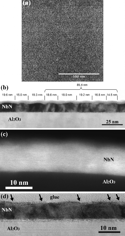
Structural characterization of the films was accomplished with scanning electron microscopy (SEM) and transmission and scanning transmission electron microscopy (TEM and STEM). SEM and TEM were carried out in either a FEI Tecnai F30 Twin S/TEM or FEI Titan 80-300 S/TEM, both operated at 300 kV. The film morphology of ENABLE-grown films is shown in Fig. 1. The SEM image in panel (a) shows the uniformity of the film in a view. The contrast giving rise to the grainy morphology arises from the 1 to 2 unit-cell deep grooves above the grain boundaries in the film. This grain boundary morphology is shown in the TEM cross-sectional view of this film in Fig. 1(b). The average thickness of the film from the TEM measurements was nm. The image was taken near a zone axis. Some of the NbN grains are crystallographically aligned to the beam to create highly-diffracting conditions and thus appear dark in the bright-field TEM images. Nearby grains misoriented by only a few degrees are not in the highly diffracting conditions and appear light in contrasts. Of particular note is the grain boundary grooving observed between these grains. The grain boundary morphology or grooving is used to define grain sizes in the other parts of the image where adjacent grains are not distinguishable by diffraction contrast. From this contrast and microstructure, we infer grain sizes in this image to be on the order of 15-20 nm. The Z-contrast STEM image of the Fig. 1(c) shows the lattice fringes of the NbN film and the ability of the film to conform to surface irregularities on the substrate. The high-resolution TEM image of Fig. 1(d) was taken from a sister sample to the sample shown in Fig. 1(a)-(c). In this image, it appears that the top layers of the substrate have been modified by the pre-nitridation step used in the film preparation. Laterally, the film interface is abrupt and well-defined. Grain boundaries can again be identified by changes in the atomic structure and the grain boundary grooving described above. Grain sizes in this image are in the 5-20 nm range and are typical of the films grown in this series. The grain boundary structures shown here are important for providing the collective pinning of the vortex lattice in the superconducting state and determine the value of the critical current, as will be revealed in the next section in the analysis of the characteristics.
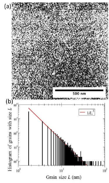
The grooving along grain boundaries can provide sufficient contrast in high magnification, plane-view SEM images to enable a much broader analysis of grain sizes in these films. An in-depth analysis of the large 1 SEM image in Fig. 1(a) is performed after converting the gray-scale image of different grain orientations to a binary black and white image in Fig. 2(a). This allows a better delineation of grains (black domains) for further identification. Because the identification of domains depends on the specific threshold used for creating a black and white image one should keep in mind that our quantitative analysis provides only an approximate count of domains that in principle should be verified by a series of TEM cross-sectional images. For a quantitative analysis of domains in the large 1 view area, we used the “Analyze Particles” method of the image tool ImageJ Rasband (2012); Ferreira and Rasband (2012); Dunes Sciences (2011) to generate a histogram of grain size area of the black domains with bins of size 10 nm2. The corresponding linear size, , histogram is shown in Fig. 2(b). varies over several orders of magnitude between 1.75 nm and 81.2 nm with a mean value of nm. The grains that were mapped onto black domains in Fig. 2(a) account for roughly 47% of the completely covered film.
The key result of the quantitative SEM analysis is that the distribution of grains is dominated by small grains, which are reasonably well described by an inverse power-law , as shown by the red solid line in Fig. 2(b). Notably the majority of grains extracted from the large view SEM image is less than 20 nm, which is consistent with the TEM cross-sections shown in Fig. 1(b) and (d). The importance of the peculiar inverse power-law will reappear in the analysis of the depinning current of the flux lattice state in Sec. III.B.
II.3 Resistivity
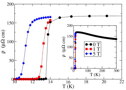
Standard film characterization was performed by transport measurements in the micron-sized wire using four-point probe technique in Physical Property Measurement System (PPMS). Figure 3 shows the resistivity data close to the superconducting transition K at zero-applied magnetic field T. was determined by the midpoint of the resistive transition, with error bars determined by the temperatures at which the resistance was at the and value of the normal state. The resistivity is in agreement with reports for thicker films in Ref. Chockalingam et al., 2008. The transition is suppressed with the field applied perpendicular to the film. At T and 5 T we observe K and K, respectively. From this field dependence we estimate for the slope of the upper critical field at the phase transition, T/K, and derive a zero-temperature coherence length nm, where is the flux quantum. In addition, in superconductors where the mean-free-path of electrons is shorter than the zero-temperature coherence length , i.e., superconductors in the dirty limit, the diffusion constant of electrons can be obtained directly from , where is the Boltzmann constant and is the negative electron charge.
We use electronic structure calculations of the electronic dispersion along high-symmetry directions to estimate the Fermi velocity in bulk NbN to be of the order km/s.Fong and Cohen (1972); Klintenberg et al. (2012); Klintenberg ; Ortiz et al. (2009) Then from the diffusion coefficient , we obtain for the mean-free-path , which is roughly three to ten times larger than reports for disordered thick films ( nm) grown by magnetron sputtering.Chand et al. (2009) We can perform a consistency check to see whether these values compare reasonably well with a rough estimation from superconducting parameters by employing . If we assume km/s, the superconducting gap meV,Hajenius et al. (2004); Chockalingam et al. (2009); Kamlapure et al. (2010) and the relation between the clean and dirty limit coherence length in superconductors de Gennes (1999) , then for the mean-free-path is nm. In conclusion, all these estimates are in agreement with each other and our earlier analysis of the film morphology of ENABLE grown NbN films, which points toward a superconductor in the dirty limit.
The inset in Fig. 3 shows the temperature dependence of the resistivity up to 300 K for a wire of size . We extract a resistivity ratio of RRR=0.83 between room temperature and slightly above , which is indicative of charge transport in a bad metal, where defect and grain boundary scattering are important. Such a scenario is consistent with a short mean-free-path and superconductivity in the dirty regime.
NbN thin films with different thickness grown on sapphire were investigated systematically in Ref. Semenov et al., 2009. For films with similar thickness, the of our samples is about K lower, while other quantities such as diffusion constant , electron mean-free-path , and zero-field superconducting critical current (see Sec. III B) are similar to those reported in Ref. Semenov et al., 2009.
III Transport measurements in the flux-flow state
In type-II superconductors () vortices enter the superconductor above the lower critical field . Under an applied DC transport current, vortices are driven by the Lorentz force perpendicular to the current, which is balanced by the pinning force in inhomogeneous superconductors as long as the transport current is smaller than the depinning current. In this case, vortices do not order into a vortex lattice state due to pinning at inhomogeneities. Finally, when the transport current exceeds the depinning current, vortices move, resulting in the flux-flow state. In the flux-flow state, the inhomogeneities in the superconductor are quickly averaged out by vortex motion and the lattice order is recovered.Koshelev and Vinokur (1994); Besseling et al. (2003)
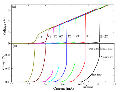
In our experiments, sample environments at fixed temperature down to 2.3 K were controlled in a Janis flow cryostat in low DC magnetic fields, from 0 to 0.1 T, generated by an electromagnet at room temperature and in a single shot fridge in an Oxford superconducting magnet with a Variable Temperature Insert for fields between 0.1 T and 15 T. The critical current measurements were carried out by means of two different pulsed techniques to avoid damage, self-heating and/or thermal runaway of the samples. We varied pulse duration and duty cycle as a mean of assessing and minimizing the self-heating. In the first method the commercial set of Keithley instruments, Nanovoltmeter Model 2128A and Model 6221 AC/DC Current Source, was used in synchrony to create the characteristic IV curves of the superconducting NbN films at fixed magnetic fields and temperatures. In the second method two waveform generators were used to create a periodic signal applied to the sample through a shunt resistor used to record the current. Voltage was measured from the corresponding sample leads, both signals were linearly amplified and stored in a scope. Both pulsed techniques show results in excellent agreement. The dimensions of the NbN film are . All transport measurements were performed at K. For our analysis we use . In addition, from the London penetration depth, nm, reported for films of similar thickness,Kamlapure et al. (2010) we deduce the Pearl length relevant for screening of magnetic flux in thin films. Typical IV curves at several magnetic fields are depicted in Fig. 4. Three different regions can be clearly seen. Below the depinning current vortices are pinned and the superconductor is in the zero-voltage state. Above the depinning current, the vortex lattice moves in the flux-flow state causing dissipation. At a critical current (voltage ) an instability occurs and the superconductor switches to the normal state. The dependence of and on the external magnetic field is nonlinear, and both decrease with field as as will be discussed below. As , and become the same and they are close to the depairing current.
III.1 Larkin-Ovchinnikov instability
The jump at is due to the instability of the collective motion of the vortex lattice as predicted by Larkin and Ovchinnikov (LO) several decades ago.Larkin and Ovchinnikov (1975) The instability is related to the quasiparticle relaxation, thus one can extract the inelastic quasiparticle relaxation time in the magnetic field from the instability. The argument for this effect is as follows: as vortices move, an electric field is induced in the normal core of vortices resulting in dissipation. Additionally, the electric field shifts the distribution of quasiparticles and pushes them outside the normal core. As a consequence, the size of the vortex core shrinks
| (1) |
where is the coherence length at the velocity of vortex and is the critical velocity of the instability. Because of the reduction of the size of the vortex core at a velocity , the Bardeen-Stephen viscosity also decreases
| (2) |
For a given Lorentz force, the increase of vortex velocity diminishes , and hence increases even further. This positive feedback speeds up the vortex motion and renders the flux-flow state unstable at a critical velocity
| (3) |
where is the quasiparticle (electron) diffusion constant with Fermi velocity . Thus one can determine by measuring the instability velocity of the flux-flow state. The LO instability of the flux-flow state has been observed both in conventional Klein et al. (1985); Samoilov et al. (1995); Ruck et al. (1997, 2000); Armenio et al. (2007); Cirillo et al. (2011) and high- cuprate superconductors.Doettinger et al. (1994, 1997)
Typical IV curves at several magnetic fields are depicted in Fig. 4. Above the depinning current , vortices move giving rise to the flux-flow state. The resistance in the flux-flow state increases with current because of the shrinkage of the vortex core as a result of the nonequilibrium LO effect. At a critical current (voltage), the system switches to the normal state. The critical velocity is given by with the voltage at the end of the flux-flow branch, the applied magnetic field, and the vacuum permeability. At higher field, the transition to the normal state becomes smooth due to the increase of vortex viscosity. We extract from the characteristics using the criteria that at the derivative jumps.
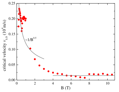
The dependence of on is shown in Fig. 5. It decreases as for a weak and then saturates at a constant value. By assuming a uniform distribution of quasiparticles in superconductors, LO predicted that the critical velocity is independent on the applied magnetic field, see Eq. (3). The uniform distribution of quasiparticles is realized at high magnetic fields where the inter-vortex distance is small, such that with . In the low magnetic field region, Eq. (3) becomes inapplicable, because the quasiparticle distribution at given by Eq. (3) is nonuniform and is confined inside the unit cell of the vortex lattice, i.e. . When the velocity of vortices increases such that quasiparticles are no longer confined in the unit cell of vortex lattice, i.e. the condition is fulfilled, the flux-flow instability is triggered Doettinger et al. (1995). Therefore in the low magnetic field region, as shown in Fig. 5. A magnetic-field independent critical velocity in the high-field region indicates that the heating effect due to vortex motion is weak and can be neglected. In the opposite case of large self-heating, it was found theoreticallyBezuglyj and Shklovskij (1992) and experimentally Kunchur (2002); Peroz and Villard (2005) that decreases as the magnetic field increases, , which is clearly not the case here.
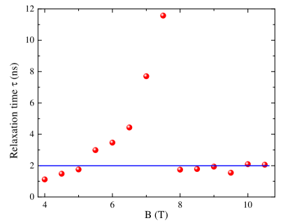
In the next step, we use Eq. (3) to find the inelastic relaxation time for quasiparticles at high fields, as shown in Fig. 6. The plateau of above 8 T is expected for flux-flow dominated by the LO instability at high fields, while the origin of the rise in between 6 T and 8 T is not understood at this time. A similar plateau in the relaxation time of NbN was reported in Ref. Cirillo et al., 2011. Obviously, for technical applications a shorter relaxation time for excited quasiparticles is preferred in order to achieve a faster response of the NbN SNSPD after the formation of a hot spot. For that reason the authors of Ref. Cirillo et al., 2011 fabricated NbN/ferromagnetic hybrids, where is two orders of magnitude smaller than in conventional NbN film due to the additional scattering channel of quasiparticles by magnetic impurities in the ferromagnetic layer, leading to a faster relaxation of excited nonequilibrium quasiparticles.
The quasiparticle relaxation time at high magnetic fields can be extracted from the LO instability of flux flow. It might be interesting to ask how the relaxation time at high fields extrapolates to the zero field case, where usually the SNSPD is operated. Recently, time-resolved, optical pump-probe measurements on a thin film show that the quasiparticle relaxation time (around 1 ns) depends weakly on the magnetic fields up to T. Zhang et al. (2006) Thus one expects that the quasiparticle relaxation time at zero magnetic field has the same order of magnitude as the one extracted from the LO instability at high fields.
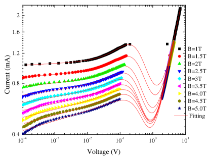
The IV curves including the LO instability can be described by the following phenomenological equation Ruck et al. (2000)
| (4) |
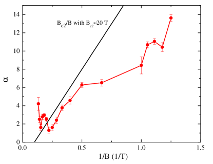
where the first term in the bracket accounts for the reduced Bardeen-Stephen viscosity in the nonequilibrium region, the second term accounts for the pinning effect, and the last term is the damping due to the suppression of superconductivity around the vortex core. Here is the normal-state resistance at and , , are fit parameters that depend on . In the limit , we should recover the linear curve for where is the Bardeen-Stephen flux-flow resistance. By expanding Eq. (4) with respect to and comparing with the linear curve, we thus obtain and . Our experimental data can be fitted very well by Eq. (4) as presented in Fig. 7. The fit parameter is shown in Fig. 8, where as expected for high fields not too close to and from the limit of . The other fit parameter is . From the fitted curves, an unstable branch of the IV curve near the LO instability becomes visible and the system develops hysteresis around the instability region. The hysteretic IV curve, due to the LO instability, has also been observed experimentally in Ref. Samoilov et al., 1995.
III.2 Vortex pinning at grain boundaries
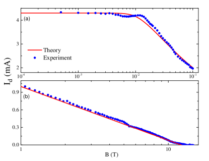
We proceed with the investigation of the depinning transition of vortices. We use the practical criterion that a depinning transition occurs when the measured voltage is larger than an arbitrary threshold of 1 mV. From that we can obtain the dependence of the depinning current on magnetic field from the IV curves. The results are compiled in Fig. 9. The depinning current depends weakly on when mT and decreases as above. It is worth to note that this logarithmic dependence cannot be explained by the collective pinning theory,Blatter et al. (1994) which predicts for thin films.
It is known from thin-film growth parameters and confirmed by TEM and SEM images that our NbN films exhibit island-like growth resulting in granular morphology. Since superconductivity is suppressed at grain boundaries, they provide a pinning potential for vortices and thus may affect SNSPD detector performance. The pinning due to grain boundaries has also been observed experimentally in high-temperature superconductor films,Fedotov et al. (2002) where the dependence of on is similar to that in Fig. 9. The depinning current density at T of our thin film is MA/cm2, which is close to the depairing current density . Thus the pinning of vortices by grain boundaries can achieve a depinning current that is close to the depairing current.
The depinning current depends crucially on the size distribution of superconducting grains (domains), which can be extracted from the dependence of on . We use a model for collective breakaway of pinned vortices developed by Fedotov et al.Fedotov et al. (2002) For simplicity we further assume square domains in our thin-film NbN. A pinning theory for more general shapes of domains was presented in Ref. Pan et al., 2006 and the results are qualitatively similar to those with square domains. One starts with a given probability density distribution of grains with linear dimension , where the probability density for a vortex inside the square domain of size is with normalization constant . The probability for finding a single vortex pinned in a domain is normalized to unity, .
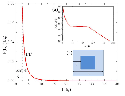
Not all vortices can sit at the energy minimum of the pinning potential due to the competition between the pining energy and elastic energy of vortex lattice. The resulting vortex configuration is a compromise between these two energies. Assuming a square pinning potential with strength and using the expression for the elastic energy of vortex lattice , we obtain the maximal displacement for pinned vortex, , i.e., if the displacement of the vortex from the grain boundary is less than , then the vortex remains pinned. Here characterizes the strength of pinning potential and is deviation from the perfect lattice. Under these conditions the vortex core gains condensation energy of superconductivity over the elastic deformation energy by staying at the grain boundary. It follows that the probability of a vortex to lie less than a distance away from the grain boundary is approximately equal to the ratio of the area of four strips of width to the total area [see the inset (b) in Fig. 10]
| (7) |
For this case it was shown that the depinning current, normalized to its value at , is simply the ratio of pinned vortices to the total number of vortices ,
| (8) | |||||
Here the magnetic field enters only through the vortex displacement .
Since a weak magnetic field corresponds to soft elastic shear stiffness of the vortex lattice, i.e., , low-field measurements probe primarily large domains, i.e. . From the measured as a function , we can obtain the distribution function from Eq. (8) by taking the third derivative with respect to to attain
| (9) |
The resulting is just the distribution function of the grain sizes . To get rid of the small oscillations in Fig. 9, we first smooth the experimental data and then use Eq. (9). The smoothed curves (not shown) are very close to the lines in Fig. 9. The resulting distribution function is shown in Fig. 10, which is in reasonable agreement with the experimental one shown in Fig. 2. The probability distribution in Fig. 10 for small grains is much larger than that for larger grains. The distribution function for small grains follows , while for large grains, it follows an exponential distribution. Since the smallest length scale for vortex is of order of , we cannot resolve the distribution for grain sizes smaller than from the measurements in the flux-flow state. Finally we confirm the agreement between the measured and calculated critical current by inserting the extracted distribution of Fig. 10 back into Eq. (8), as shown in Fig. 9.
IV Summary
In summary, we characterized the quality and uniformity of ENABLE-grown thin-film NbN superconductors for potential SNSPD applications. From transport measurements we derived superconducting material parameters K, nm, and depinning current density MA/cm2. In addition, we determined that our thin films of thickness nm are in the dirty limit with the mean-free-path much shorter than the coherence length of the hypothetically clean superconductor, . This length scale was further corroborated by the distribution of grain sizes extracted from the analysis of SEM and TEM images and the field-dependence of depinning currents. The presented vortex theory successfully explained the collective vortex lattice motion in the flux-flow state with the Larkin-Ovchinnikov instability in the characteristics at high bias currents, as well as the depinning current at low bias currents. The detailed analysis of the Larkin-Ovchinnikov instability revealed a relatively long inelastic quasiparticle relaxation lifetime of order ns, which might provide the bottleneck for the hot spot relaxation in NbN-based SNSPD devices. Finally, from the nondestructive measurement of the depinning current with magnetic fields, we extracted the characteristic domain size distribution of grains, which resulted in comparable values to the independent, yet destructive, analysis using TEM techniques. While the prevalence of grain boundaries in thin-film NbN superconductors crucially affects transport properties like critical currents, their potential for vortex pinning at low bias currents is negligible for SNSPD applications, which are typically biased close to the critical current. This study has shown the potential use of field-dependent measurements of the depinning current in micron-sized wires for determining the grain size distribution in thin-film superconductors. The advantage of a nondestructive characterization method of the uniformity of thin superconducting films may prove beneficial for the pre-screening of films for further nano-patterning.
V Acknowledgement
This work was performed under the auspices of the U.S. DOE contract No. DE-AC52-06NA25396 through the LDRD program at Los Alamos National Laboratory, the Center for Integrated Nanotechnologies, an Office of Science User Facility operated for the U.S. DOE, and the National High Magnetic Field Laboratory, which is jointly supported by the U.S. DOE, NSF, and the State of Florida.
References
- Il’in et al. (2000) K. S. Il’in, M. Lindgren, M. Currie, A. D. Semenov, G. N. Gol’tsman, R. Sobolewski, S. I. Cherednichenko, and E. M. Gershenzon, Appl. Phys. Lett. 76, 2752 (2000).
- Gol’tsman et al. (2001) G. N. Gol’tsman, O. Okunev, G. Chulkova, A. Lipatov, A. Semenov, K. Smirnov, B. Voronov, A. Dzardanov, C. Williams, and R. Sobolewski, Appl. Phys. Lett. 79, 705 (2001).
- Romestain et al. (2004) R. Romestain, B. Delaet, P. Renaud-Goud, I. Wang, C. Jorel, J. Villegier, and J. Poizat, New J. Phys. 6, 129 (2004).
- Kerman et al. (2006) A. J. Kerman, E. A. Dauler, W. E. Keicher, J. K. W. Yang, K. K. Berggren, G. Gol’tsman, and B. Voronov, Appl. Phys. Lett. 88, 111116 (2006).
- Kitaygorsky et al. (2005) J. Kitaygorsky, J. Zhang, A. Verevkin, A. Sergeev, A. Korneev, V. Matvienko, P. Kouminov, K. Smirnov, B. Voronov, G. Gol’tsman, and R. Sobolewski, IEEE Trans. Appl. Supercond. 15, 545 (2005).
- Kitaygorsky et al. (2007) J. Kitaygorsky, I. Komissarov, A. Jukna, D. Pan, O. Minaeva, N. Kaurova, A. Divochiy, A. Korneev, M. Tarkhov, B. Voronov, I. Milostnaya, G. Gol’tsman, and R. Sobolewski, IEEE Trans. Appl. Supercond. 17, 275 (2007).
- Miki et al. (2008) S. Miki, M. Fujiwara, M. Sasaki, B. Baek, A. J. Miller, R. H. Hadfield, S. W. Nam, and Z. Wang, Appl. Phys. Lett. 92, 061116 (2008).
- Annunziata et al. (2009) A. J. Annunziata, D. F. Santavicca, J. D. Chudow, L. Frunzio, M. J. Rooks, A. Frydman, and D. E. Prober, IEEE Trans. Appl. Supercond. 19, 327 (2009).
- Baek et al. (2011) B. Baek, A. E. Lita, V. Verma, and S. W. Nam, Appl. Phys. Lett. 98, 251105 (2011).
- Clem and Berggren (2011) J. R. Clem and K. K. Berggren, Phys. Rev. B 84, 174510 (2011).
- Il’in et al. (2012) K. Il’in, M. Hofherr, D. Rall, M. Siegel, A. Semenov, A. Engel, K. Inderbitzin, A. Aeschbacher, and A. Schilling, J. Low Temp. Lett. 167, 809 (2012).
- Hofherr et al. (2012) M. Hofherr, D. Rall, K. Il’in, A. Semenov, H.-W. Hübers, and M. Siegel, J. Low Temp. Phys. 167, 822 (2012).
- Engel et al. (2012) A. Engel, A. Schilling, K. Il’in, and M. Siegel, Phys. Rev. B 86, 140506(R) (2012).
- Natarajan et al. (2012) C. M. Natarajan, M. G. Tanner, and R. H. Hadfield, Supercond. Sci. Technol. 25, 063001 (2012).
- Marsili et al. (2012a) F. Marsili, F. Bellei, F. Najafi, A. E. Dane, E. A. Dauler, R. J. Molnar, and K. K. Berggren, Nano Lett. 12, 4799 (2012a).
- Yang et al. (2007) J. K. Yang, A. J. Kerman, E. A. Dauler, V. Anant, K. M. Rosfjord, and K. K. Berggren, IEEE Trans. Appl. Supercond. 17, 581 (2007).
- Kerman et al. (2009) A. J. Kerman, J. K. W. Yang, R. J. Molnar, E. A. Dauler, and K. K. Berggren, Phys. Rev. B 79, 100509 (2009).
- Marsili et al. (2012b) F. Marsili, F. Najafi, E. Dauler, R. J. Molnar, and K. K. Berggren, Appl. Phys. Lett. 100, 112601 (2012b).
- Bartolf et al. (2010) H. Bartolf, A. Engel, A. Schilling, K. Il’in, M. Siegel, H. Hübers, and A. Semenov, Phys. Rev. B 81, 024502 (2010).
- Yamashita et al. (2011) T. Yamashita, S. Miki, K. Makise, W. Qiu, H. Terai, M. Fujiwara, M. Sasaki, and Z. Wang, Appl. Phys. Lett. 99, 161105 (2011).
- Sclafani et al. (2012) M. Sclafani, M. Marksteiner, F. M. Keir, A. Divochiy, A. Korneev, A. Semenov, G. Gol’tsman, and M. Arndt, Nanotechn. 23, 065501 (2012).
- Inderbitzin et al. (2012) K. Inderbitzin, A. Engel, A. Schilling, K. Il’in, and M. Siegel, Appl. Phys. Lett. 101, 162601 (2012).
- Semenov et al. (1995) A. D. Semenov, R. S. Nebosis, Y. P. Gousev, M. A. Heusinger, and K. F. Renk, Phys. Rev. B 52, 581 (1995).
- Engel et al. (2006) A. Engel, A. Semenov, H. Hübers, K. Il’in, and M. Siegel, Physica C 444, 12 (2006).
- Bulaevskii et al. (2011) L. N. Bulaevskii, M. J. Graf, C. D. Batista, and V. G. Kogan, Phys. Rev. B 83, 144526 (2011).
- Bulaevskii et al. (2012) L. N. Bulaevskii, M. J. Graf, and V. G. Kogan, Phys. Rev. B 85, 014505 (2012).
- Kaplan et al. (1976) S. B. Kaplan, C. C. Chi, D. N. Langenberg, J. J. Chang, S. Jafarey, and D. J. Scalapino, Phys. Rev. B 14, 4854 (1976).
- Rasband (2012) W. S. Rasband, ImageJ - http://imagej.nih.gov/ij (U.S. National Institutes of Health, Bethesda, Maryland, USA, 2012).
- Ferreira and Rasband (2012) T. Ferreira and W. S. Rasband, ImageJ User Guide - IJ1.46 (U.S. National Institutes of Health, http://imagej.nih.gov/ij/docs/guide, 2012).
- Dunes Sciences (2011) Dunes Sciences, Particle Size Analysis - Standard Operating Protocol (Dunes Sciences, Inc, 2011).
- Williamson et al. (2011a) T. L. Williamson, J. J. Williams, J. C. D. Hubbard, and M. A. Hoffbauer, 29, 03C132 (2011a).
- Williamson et al. (2011b) T. L. Williamson, A. L. Salazar, J. J. Williams, and M. A. Hoffbauer, Phys. Stat. Sol. C 8, 2098 (2011b).
- Mueller et al. (2006) A. H. Mueller, E. A. Akhadov, and M. A. Hoffbauer, Appl. Phys. Lett. 88, 041907 (2006).
- Chockalingam et al. (2008) S. P. Chockalingam, M. Chand, J. Jesudasan, V. Tripathi, and P. Raychaudhuri, Phys. Rev. B 77, 214503 (2008).
- Fong and Cohen (1972) C. Y. Fong and M. L. Cohen, Phys. Rev. B 6, 3633 (1972).
- Klintenberg et al. (2012) M. Klintenberg, J. T. Haraldsen, and A. V. Balatsky, VIZ@CINT (Center for Integrated Nanotechnologies User Project, 2012).
- (37) M. Klintenberg, The Electronic Structure Project.
- Ortiz et al. (2009) C. Ortiz, O. Eriksson, and M. Klintenberg, Comput. Mater. Sci. 44, 1042 (2009).
- Chand et al. (2009) M. Chand, A. Mishra, Y. M. Xiong, A. Kamlapure, S. P. Chockalingam, J. Jesudasan, V. Bagwe, M. Mondal, P. W. Adams, V. Tripathi, and P. Raychaudhuri, Phys. Rev. B 80, 134514 (2009).
- Hajenius et al. (2004) M. Hajenius, J. J. A. Baselmans, J. R. Gao, T. M. Klapwijk, P. A. J. d. Korte, B. Voronov, and G. Gol tsman, Supercond. Sci. Technol. 17, S224 (2004).
- Chockalingam et al. (2009) S. P. Chockalingam, M. Chand, A. Kamlapure, J. Jesudasan, A. Mishra, V. Tripathi, and P. Raychaudhuri, Phys. Rev. B 79, 094509 (2009).
- Kamlapure et al. (2010) A. Kamlapure, M. Mondal, M. Chand, A. Mishra, J. Jesudasan, V. Bagwe, L. Benfatto, V. Tripathi, and P. Raychaudhuri, App. Phys. Lett. 96, 072509 (2010).
- de Gennes (1999) P. G. de Gennes, Superconductivity of Metals and Alloys (Westview Press, Boulder CO, 1999) Chap. 7.
- Semenov et al. (2009) A. Semenov, B. Günther, U. Böttger, H.-W. Hübers, H. Bartolf, A. Engel, A. Schilling, K. Ilin, M. Siegel, R. Schneider, D. Gerthsen, and N. A. Gippius, Phys. Rev. B 80, 054510 (2009).
- Koshelev and Vinokur (1994) A. E. Koshelev and V. M. Vinokur, Phys. Rev. Lett. 73, 3580 (1994).
- Besseling et al. (2003) R. Besseling, N. Kokubo, and P. H. Kes, Phys. Rev. Lett. 91, 177002 (2003).
- Larkin and Ovchinnikov (1975) A. I. Larkin and Y. N. Ovchinnikov, Sov. Phys. JETP 41, 960 (1975).
- Klein et al. (1985) W. Klein, R. P. Huebener, S. Gauss, and J. Parisi, J. Low Temp. Phys. 61, 413 (1985).
- Samoilov et al. (1995) A. V. Samoilov, M. Konczykowski, N. C. Yeh, S. Berry, and C. C. Tsuei, Phys. Rev. Lett. 75, 4118 (1995).
- Ruck et al. (1997) B. J. Ruck, J. C. Abele, H. J. Trodahl, S. A. Brown, and P. Lynam, Phys. Rev. Lett. 78, 3378 (1997).
- Ruck et al. (2000) B. J. Ruck, H. J. Trodahl, J. C. Abele, and M. J. Geselbracht, Phys. Rev. B 62, 12468 (2000).
- Armenio et al. (2007) A. A. Armenio, C. Bell, J. Aarts, and C. Attanasio, Phys. Rev. B 76, 054502 (2007).
- Cirillo et al. (2011) C. Cirillo, V. Pagliarulo, H. Myoren, C. Bonavolontà, L. Parlato, G. P. Pepe, and C. Attanasio, Phys. Rev. B 84, 054536 (2011).
- Doettinger et al. (1994) S. G. Doettinger, R. P. Huebener, R. Gerdemann, A. Kuhle, S. Anders, T. G. Trauble, and J. C. Villegier, Phys. Rev. Lett. 73, 1691 (1994).
- Doettinger et al. (1997) S. G. Doettinger, S. Kittelberger, R. P. Huebener, and C. C. Tsuei, Phys. Rev. B 56, 14157 (1997).
- Doettinger et al. (1995) S. G. Doettinger, R. P. Huebener, and A. Kühle, Physica C 251, 285 (1995).
- Bezuglyj and Shklovskij (1992) A. I. Bezuglyj and V. A. Shklovskij, Physica C 202, 234 (1992).
- Kunchur (2002) M. N. Kunchur, Phys. Rev. Lett. 89, 137005 (2002).
- Peroz and Villard (2005) C. Peroz and C. Villard, Phys. Rev. B 72, 014515 (2005).
- Zhang et al. (2006) H. Zhang, H. Tashiro, R. P. S. M. Lobo, D. H. Reitze, C. J. Stanton, D. B. Tanner, and G. L. Carr, AIP Conference Proceedings 850, 981 (2006).
- Werthamer et al. (1966) N. R. Werthamer, E. Helfand, and P. C. Hohenberg, Phys. Rev. 147, 295 (1966).
- Blatter et al. (1994) G. Blatter, M. V. Feigelman, V. B. Geshkenbein, A. I. Larkin, and V. M. Vinokur, Rev. Mod. Phys. 66, 1125 (1994).
- Fedotov et al. (2002) Y. V. Fedotov, S. M. Ryabchenko, E. A. Pashitskii, A. V. Semenov, V. I. Vakaryuk, V. M. Pan, and V. S. Flis, Low Temp. Phys. 28, 172 (2002).
- Pan et al. (2006) V. Pan, Y. Cherpak, V. Komashko, S. Pozigun, C. Tretiatchenko, A. Semenov, E. Pashitskii, and A. V. Pan, Phys. Rev. B 73, 054508 (2006).