Now at ]University of New South Wales, Australia
Magnetotransport and induced superconductivity in Bi based three-dimensional topological insulators
Abstract
The surface of a 3D topological insulator is conducting and the topologically nontrivial nature of the surface states is observed in experiments. It is the aim of this paper to review and analyze experimental observations with respect to the magnetotransport in Bi-based 3D topological insulators, as well as the superconducting transport properties of hybrid structures consisting of superconductors and these topological insulators. The helical spin-momentum coupling of the surface state electrons becomes visible in quantum corrections to the conductivity and magnetoresistance oscillations. An analysis will be provided of the reported magnetoresistance, also in the presence of bulk conductivity shunts. Special attention is given to the large and linear magnetoresistance. Superconductivity can be induced in topological superconductors by means of the proximity effect. The induced supercurrents, Josephson effects and current-phase relations will be reviewed. These materials hold great potential in the field of spintronics and the route towards Majorana devices.
I Introduction
A three-dimensional (3D) topological insulator (TI) is a semiconductor with two-dimensional (2D) surface states that have an energy dispersion across the entire bulk bandgap. These surface states arise from band inversion, due to strong spin-orbit interactions. The band inversion makes the surface states topologically nontrivial, meaning that these states are protected (cannot be removed) and that the states have a helical Dirac-type dispersion, where spin is tightly coupled to momentum. Several compounds have been theoretically predicted to be 3D TIs Fu2007a . Strong experimental evidence for the presence of topological surface states exists for the class of Bi-based materials: the alloy Bi1-xSbx Fu2007b , and the compounds Bi2Se3 and Bi2Te3 Zhang2009 , see Fig. 1 for the crystal structure. The class of Bi-based topological insulator has been expanded with the fabrication of TlBiSe2 Sato2010 ; Kuroda2010 ; Chen2010b , TlBiTe2 Chen2010b , BiSbPbTe Souma2012 , and PbBiTe4 Kuroda2012 . The bulk of these compounds is not necessarily insulating, due to the presence of defects and impurities. This bulk conductivity might shunt and mask topological transport properties. A successful trend in the research on topological insulators has been to reduce the number of defects and impurities by atom substitutions such as Bi2Te2SeXu2010 ; Ren2010 ; Xiong2011 and Bi2-xSbxTe3-ySey Ren2011 . which have higher bulk resistivities. Simultaneously, progress has been made in disentangling topological surface state transport properties from bulk transport contributions.
Here, we review and analyze the experimentally observed magnetotransport properties of the Bi based 3D TIs as well as the induced superconductivity in these compounds. Studying transport properties in an externally applied large magnetic field is a powerful probe of the topological nature of the surface states. A Berry phase shift appears in magnetoresistance oscillations and in quantum corrections to the conductivity, leading for example to weak anti-localization effects. We will review the ongoing debate on the manifestation of this phase shift and show how the phase shift depends on the actual parameters of the sample. We will discuss the important role of bulk conductivity contributions. Intriguingly, two-dimensional transport features not always originate from the surface in Bi-based topological insulators. This finding is also important for understanding the presence of a large and linear magnetoresistance in most Bi-based 3D TIs.
The topologically non-trivial surface state is an attractive medium to study unconventional superconductivity. When superconductivity exists in a system with a Dirac-type dispersion and helical spin-momentum locking, exotic features could be realized such as -wave order parameter symmetry Kitaev2001 and Majorana type bound states Fu2008 . Josephson hybrid structures have been designed theoretically already to mimic non-abelian particle statistics Fu2008 . Parallel to the trend of doping and alloying TIs to render them superconducting Sasaki2011 ; Heumen2012 runs the successful approach of inducing superconductivity from a standard superconductor into a TI by means of the proximity effect. Here, we will review the current status of the experimental efforts in the latter direction. Evidence for supercurrents through topological surface states will be analyzed, also in the presence of bulk conducting channels. The prospects for future SQUID based experiments to detect topological effects in the superconductivity will be discussed.
II Weak antilocalization
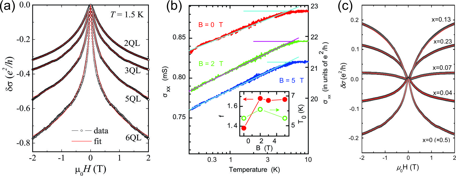
Weak antilocalization (WAL) is commonly observed in magnetoresistance measurements on thin films or flakes of Bi-based 3D TIs, see Fig. 2(a). WAL is observed for a wide range of thicknesses. Kim et al.Kim2011 report magnetotransport on BiTe films from 3 nm to 170 thick, where they can still see the WAL effect. When caused by topological surface state transport, WAL may more properly be named topological delocalizationLiu2011 , because the antilocalization is caused by the -Berry phase (see section 3) picked up along two time-reversed self-intersecting paths. Effectively, in TI surface states all the WL orbits contribute as WAL orbits. WL will not appear in TIs, as long as time reversal symmetry is not broken.
The Hikami-Larkin-Nagaoka (HLN) equationHikami1980 describes the quantum correction to 2D conductivity due to (anti-)localization effects as
| (1) |
where is the digamma function, , and is the dephasing length. Strong spin-orbit interactions (or topological effects) give WAL with while weak spin-orbit scattering typically gives weak localization (WL) effects with . A logarithmic temperature dependence is expected, since generally scales inversely with temperature. For WL the conductivity decreases with decreasing temperature and for WAL the conductivity increases with decreasing temperature. An applied magnetic field will reduce the effect of the quantum corrections, due to a phase being picked up in the magnetic field, destroying the interference effects. Equation (1) is an approximation of an expression that takes all the scattering lengths explicitly into account Hikami1980 .
For topological insulator devices, the value of in Eq. (1) is usually around , but it is found to depend on sample thickness, the presence of bulk conductivity, gating and the substrate, as will be elaborated below. The trivial value of is only found for higher temperatures or for very thin samples in a parallel applied field He2011 . Depending on the number of conduction channels, can even become when both the top and the bottom surface of a crystal or film contribute independently Zhang2011a ; Steinberg2011 ; Checkelsky2011 . The 2D nature of the WAL is confirmed by angle dependent measurements. For a 2D system, the WAL effect only depends on the perpendicular component of the field He2011 ; Cha2012a . For higher fields extra spin effects may arise due to the Zeeman splitting caused by the parallel field Iordanskii1994 ; Meijer2005 .
II.1 Bulk vs surface
Even when the 2D nature of the WAL is confirmed by angle dependent measurements, the WAL can still be caused by bulk effects. Quite a number of reports Kim2011 ; Liu2011 ; He2011 ; Zhang2011a ; Steinberg2011 ; Wang2011 ; Takagaki2012 ; Zhang2012 ; Chen2010 ; Chen2011 ; Taskin2012 ; Gao2012 deduce a dephasing length from the WAL fit using the HLN-equation that is larger than the film thickness, making the bulk effectively more 2D. Also, it is an intriguing question why in most cases the observed WAL can only be explained by just one of the two surfaces (i.e. ). One option would be that the whole topological insulator can be considered as one 2D system with spin-orbit coupling, as a mix of bulk channels and surface states He2011 ; Zhang2011a ; Steinberg2011 ; Chen2011 ; Taskin2012 . The question then is how these contributions can be disentangled. An answer might be found in the hints of bulk contribution found in some works, such as a broader WAL from the bulk Cha2012a , WL channels Zhang2012b ; Lu2011 ; Garate2012 or by specifically trying to influence the surface states, for example by gating Zhang2011a ; Steinberg2011 ; Checkelsky2011 ; Gao2012 or by introducing magnetic particles He2011 . A theoretical description of the bulk-surface coupling is given by Refs. Lu2011 and Garate2012 .
He et al. He2011 show that the WAL in Bi2Te3 thin films has contributions from both the surface and the bulk, by analyzing angle dependent measurements. The surface contribution to the WAL can be suppressed by depositing magnetic impurities (Fe) on the surface. For very thin films they observe a crossover to the regime of a field dependence. The question does arise what happens to the bottom interface; the film is smaller than the phase coherence length and the bottom interface should not be affected by the magnetic impurities on the top interface. The authors note that the contributions from the bottom surface seem negligible and that this may be caused by defects present at the TI-substrate interface. Checkelsky et al. Checkelsky2011 find contributions from two interfaces using the HLN equation to fit the WAL measured on exfoliated flakes of Bi2Se3, while still having a phase coherence length larger than the thickness of the flakes. This gives merit to the claim that for grown thin films, the bottom interface has too much disorder to show a WAL effect He2011 .
Steinberg et al. Steinberg2011 observe a tunability of the number of channels leading to WAL in top gate tuned 20 nm Bi2Se3 thin films, both by temperature and applied electric field. The authors argue that the different channels can be viewed as independent as long as carriers in one channel lose coherence before scattering to the other channel, i.e. , where is the surface-to-bulk scattering time. This can be the case when a depletion layer is formed between the surface and the bulk by applying a gate voltage Zhang2011a ; Steinberg2011 ; Checkelsky2011 ; Chen2011 ; Gao2012 . Steinberg et al. Steinberg2011 observe that the HLN fit also works in the crossover regime between and , indicating that, while there is no theoretical model, can be used as a phenomenological measure for the channel separation (i.e. the ratio ). As the temperature is increased the channel separation is seen to increase, which is explained by the strong temperature dependence of versus the relatively temperature independent , which is suggested to be governed by impurity scattering Steinberg2010 . A similar empirical model is suggested by Kim et al. Kim2011 . In their measurements on up to 100 unit cells of Bi2Se3, the mobility depends linearly on the film thickness, indicating that should also depend linearly on film thickness if the WAL would be a purely bulk effect. However, in the thin film limit the scaling of deviates from a linear scaling, indicating it cannot be explained by only a bulk contribution. The authors note that the scaling of with thickness can be used as a figure of merit for TIs. For , should be zero for a perfect TI with insulating bulk, one for a trivial strong spin-orbit coupling material or somewhere in between for a TI with both surface and bulk contribution.
II.2 Localization to antilocalization crossover
A combination of WL and WAL is observed at low temperatures in ferrocene doped Bi2Se3 nanoribbons Cha2012a . This can be explained by the opening of a band gap in the surface states induced by the magnetic impurities Lu2011a or by a canceling of the bulk spin-orbit coupling by the magnetic impurities Cha2012a . A more detailed study with controlled magnetic doping is needed to disentangle these two effects. A coexistence of WL and WAL for nonmagnetic dopants has not been observed He2011 ; Cha2012a ; Cha2012 , which is an indication that (a significant portion of) the WAL is caused by the topologically protected surface states.
Liu et al. Liu2012 observe a crossover as a function of Cr doping in Bi2Se3 films of 3 unit cell quintuple layers (QL) grown by molecular beam epitaxy on sapphire, see Fig. 2(c). While this thickness is already in the regime where scattering between the two surfaces opens up a gap in the surface states Zhang2010 , the authors note that the observed effects are still nominally the same as in 6 QL films, but without a quadratic bulk contribution. The crossover looks similar to what has been predicted theoreticallyLu2011a , driven by the opening of a gap due to the magnetic impurities Liu2009 ; Chen2010a . However, the authors note that from their ARPES measurements, it looks like the surface states completely disappear for large magnetic doping, leaving the system in a dilute magnetic semiconductor state. They find for the HLN fit for the highly doped films, which is indeed closer to the regime of strong magnetic scattering than the WL regime Hikami1980 . The authors observe a further crossover as a function of temperature, where for the highly doped samples there is a coexistence of WL and WAL, each with a different critical field scale Liu2012 . This coexistence could be another explanation for the low value of ; in the crossover regime the limiting cases used to obtain Eq. (1) do not hold and the full expression should be used Hikami1980 ; Bergmann1984 .
II.3 Electron-electron interactions
Electron-electron interactions (EEI) can lower the conductivity via the Aronov-Altshuler effect Altshuler1979 ; Lee1985 . The Coulomb interaction between different electrons decreases the effective density of states near the Fermi energy, which results in a correction to the conductivity that is logarithmic in temperature. In magnetic fields the conductivity will further decrease as a result of Zeeman splittingLee1985 .
The correction to the conductivity by EEI Lee1985 is given by
| (2) |
where is the Coulomb screening factor and is the characteristic temperature for EEI effects.
EEI is used by some authors Liu2011 ; Takagaki2012 ; Checkelsky2009 to explain a decrease in conductance that depends logarithmically on temperature, where an increase is expected for just WAL. This decrease is not always observed: in some cases there is only a metallic temperature dependence Zhang2011a ; Taskin2012 . EEI have already been used to explain localization effects in other strong spin-orbit materials Beutler1988 ; Lin1987 . The EEI contribution to conductivity is extracted from the conductance in magnetic fields.
Checkelsky Checkelsky2009 deduce both orbital and spin contributions to the magnetotransport from the angle dependence of universal conductance fluctuations. The low field effect is fit by a combination of WAL Hikami1980 (the orbital part) and EEI Lee1985 (the spin part). They find a logarithmic field dependence, but the fitting parameters are orders of magnitude larger than expected for a 2D system. The authors reason that extra 2D bulk states with similar spin-orbit properties as the surface states may be able to explain this discrepancy Analytis2010a .
Takagaki Takagaki2012 determine the prefactor and in Eq. (2) by looking at the temperature dependence in magnetic fields, to suppress the contribution of WAL, see Fig. 2(b). The value they find for the screening factor is too large to only come from the surface, which suggests that the bulk states also have to be taken into account.
Liu Liu2011 observe a combination of WAL and EEI in ultrathin Bi2Se3 films of one to six QL grown on sapphire. The logarithmic temperature dependence is determined to be caused by EEI by studying the MR in parallel fields. EEI is largely field independent, but for large Zeeman splitting it will be suppressed with a logarithmic field dependence. The g-factor is not very large in TIs Xiong2012a , but Liu indeed observe a logarithmic field dependence for fields above 4 T. They argue that the EEI becomes larger for thinner films due to increased disorder and reduced dimensionality, leading to poorer screening and therefore stronger Coulomb interaction Liu2011 .
III Shubnikov-de-Haas oscillations and Berry phase
The mobility of the Bi-based topological insulators has frequently been reported to be high enough to fulfill the condition , where Shubnikov-de-Haas oscillations can be observed in the resistance at high magnetic fields Ren2010 ; Taskin2012 ; Xiong2012a ; Qu2010 ; Taskin2010 ; Analytis2010 ; Sacepe2011 ; Brune2011 ; Xiu2011 ; Taskin2011b ; Xiong2012 ; Veldhorst2012a ; Cao2012 ; Ren2011r ; Ren2012 . The oscillations in the longitudinal surface resistance are given Lifshitz1956 by
| (3) |
where is a Berry phase, as will be discussed below, and the frequency is determined from the extremal cross-section of the Fermi surface, .
If the electron orbit is confined to a 2D plane as for a two-dimensional electron gas, then is the perpendicular magnetic field component. However, a cosine magnetic field angle dependence of the oscillations alone is not enough to conclude that the topological surface states are providing the oscillations. For example, it has been shown for Bi2Se3 that the bulk may act as the sum of many parallel 2D electron systems Cao2012 . And a surface state might also be a non-topological trivial band that crosses the Fermi energy due to band bending at the surface, as observed for Bi1.5Sb0.5Te1.7Se1.3 Taskin2011b .
Rather, the topological nature can be concluded from the phase of the Shubnikov-de-Haas oscillations. From graphene it is known how a Dirac cone gives rise to a half filled Landau level at zero energy (here defined as the energy of the Dirac point) and how this Landau level gives an additional Berry phase shift of to the quantum Hall effect or Shubnikov-de-Haas oscillations Novoselov2005 ; Zhang2005 . In general, the Berry phase can be obtained by integrating the Berry connection over an electron orbit
| (4) |
where the Berry connection follows from a specific band structure as
| (5) |
where are the periodic parts of the Bloch wave functions. It turns out that Eq. (4) gives at the surface of the Bi-based topological insulators irrespective of the exact shape of the Dirac cone Mikitik2012 , i.e. deviations of the linear dispersion in a Dirac cone do not lead to different values for the Berry phase, in contrast to previous expectations Taskin2011 . The crucial ingredient to have a Berry phase is that the order of conduction band and valence band are inverted due to strong spin-orbit coupling.
For the trivial case, Eq. (3) shows that the magnetoresistance oscillations have a minimum in the limit . A plot of the positions as function of the number of minima then extrapolates to 0. When , the positions of the minima extrapolate to . The extrapolation becomes very accurate either when the applied magnetic fields are so large that the lowest Landau levels are resolved, or when an additional gate voltage is used to sweep the Fermi energy Sacepe2011 .
Inverting the resistivity tensor gives the longitudinal conductivity as . In a one-band free electron model, the oscillation condition coincides with since and , where is the carrier density. When the oscillations in are small () and when oscillations in can be neglected, the fulfilled condition automatically ensures that , i.e. the oscillations in conductivity and resistivity are in phase. Both and have minima at integer Landau level index . Magnetic field measurements on semiconductors are usually in this regime.
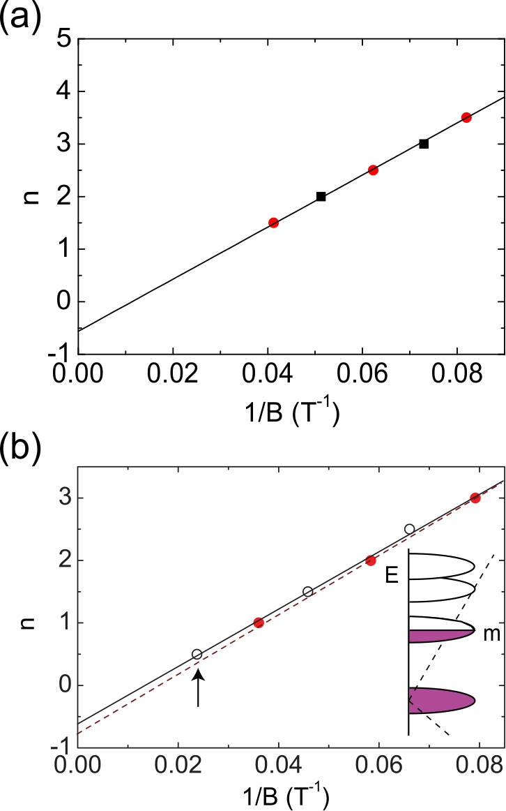
However, in the presence of a bulk shunt with a low mobility, the oscillations in and can be out of phase. It was shown for a Bi2Te2Se crystal showing bulk conductivity with a low mobility that the surface state resistivity has maxima now at integer Xiong2012a . Consequently, the Berry phase needs to be inferred from a plot of the maxima positions at integer , see Fig. 3(b), where the topologically non-trivial was observed. However, this situation Xiong2012a is not generic for any strong bulk conductivity shunt. In a parallel summation of surface and bulk conductivity, it can be shown that and are in phase when the bulk mobility is not too low, i.e. as long as . For example, Cao et al. Cao2012 have shown that the bulk in highly doped Bi2Se3 can act as the sum of many parallel layers with high mobility and a trivial Berry phase with minima at integer . Lower bulk densities will enhance the surface state conduction. In Fig. 3(a) data is shown for a 100 nm thick exfoliated flake of Bi2Te3. A multiband analysis (assuming two surfaces and one bulk channel) of the Hall data and Shubnikov de Haas oscillations of Ref. Veldhorst2012a provides a bulk carrier density of cm-3 and a bulk mobility of the order of 0.1 m2V-1s-1, so that is fullfilled above about 10 T. The extrapolation of the minima in at integer consistentently extrapolate to again. For every sample with bulk conductivity a detailed parameter estimate should decide in which regime the oscillations are and whether maxima or minima positions should be considered.
IV Linear magnetoresistance
In addition to quantum transport phenomena such as Shubnikov-de Haas oscillations and weak antilocalisation, a strong background magnetoresistance (MR) was also observed in the 3D TIs Bi2Te3 Qu2010 ; Wang2012 , Bi2Se3 Zhang2011a ; Tang2011 ; He2012 ; Gao2012 , and Bi2Te2Se Assaf2012 . The reported magnetoresistance varies from a few percent to more than 600% Wang2012 . In contrast to the more standard small quadratic MR (e.g. due to multiband effects), which saturates for , the observed MR is linear with field and does not seem to saturate in high fields. The MR is positive, also for negative field directions, thereby ruling out Hall component admixtures due to misaligned electrodes.
Linear MR is not a new phenomenon and was already observed about 100 years ago in Bi Kapitza1928 ; Abrikosov2000 . The so-called Kapitza linear MR as observed in metals with open Fermi surfaces require large Fermi areas (and therefore large carrier densities) and this does not really apply to any of the Bi-based 3D TIs of current interest. Moreover, more quantitative treatments of open orbits seem to indicate or rather than linear behavior. Abrikosov proposed a quantum MR model to account for linear MR Abrikosov2000 ; Abrikosov1969 ; Abrikosov1998 when only one Landau magnetic band is filled. The conditions for the sole occupation of the lowest Landau level (at energy ) is that both the Fermi energy, , and are much smaller than , where is the energy of the next Landau level. This is called the extreme quantum limit and the resulting linear MR is called quantum linear MR.
Usually, the conditions for the extreme quantum limit are only fulfilled for narrow gap semiconductors or semi-metals with very small Fermi pockets and low effective masses. Examples are Bi, n-type doped InSb Hu2008 , and PbS Eto2010 . For a parabolic dispersion, the Landau levels are given by . A low effective mass gives a large cyclotron frequency, and a large spacing between Landau levels. Entering the extreme quantum limit is also facilitated in materials with a linear dispersion. E.g., for -Ag2Te a linear MR was observed for fields as low as 10 Oe at 4.5 K Xu1997 , for which the conditions of the extreme quantum limit do not seem to be fulfilled ( for Oe and gives K). However, for a material with linear dispersion, the Landau levels are given by , where is the Dirac velocity. This provides a less stringent condition for the extreme quantum limit at 10 Oe ( K for m/s). Recently, it has been calculated that -Ag2Te is indeed a material with a linear dispersion Zhang2011c .
Apart from a single Landau level explaining linear MR, also inhomogeneities in disordered conductors can give rise to linear MR. This is described by the model of Parish and Littlewood Parish2003 ; Parish2005 . Regions with higher conductivity create deviations of the direction of the applied current and classical resistor network models show that also in this case a Hall voltage admixture occurs, giving rise to a linear MR Parish2003 ; Parish2005 . The Hall signal mixes in such a way that the MR is still symmetric in field. The magnitude of the magnetoresistance from this effect will not exceed the maximum local Hall resistance in the inhomogeneous system. Note, that also the classical inhomogeneity model was used to explain the -Ag2Te linear MR Parish2003 .
The nature of the linear magnetoresistance in topological insulators is not clear yet. In the past few years a lot of research has focused on unraveling the mechanism behind this linear magnetoresistance and to investigate which model applies and whether or not linear MR is a signature of the topological surface states. Furthermore, unravelling the origin of the linear magnetoresistance can have important consequences for spintronics, as the observed magnetoresistance is already large in amplitude and survives even up to room temperature.
IV.1 Bulk vs surface
Qu Qu2010 found a magnetoresistance of 1.7% at 0.3 K in a magnetic field of 14 T in Bi2Te3 crystals. The observed dependence on perpendicular field is linear, starting already from a very small magnetic field of 30 G. The in-plane MR is also linear, but the effect is a factor of 2 smaller than for perpendicularly applied field. The authors attributed the MR to the coupling of the spin of the bulk electrons to the magnetic field. It is interesting to note that the linear magnetoresistance (LMR) in this case was only observed in the non-metallic samples, while the metallic sample showed quadratic MR. Furthermore, besides the LMR also Shubnikov-de Haas oscillations were observed for the out-of-plane field.
The angular dependence of the LMR was investigated Tang2011 ; He2012 . By changing the direction of the field from out-of-plane to in-plane, the LMR decreased significantly and a relation was found between the LMR and angle of the field. This indicates that the LMR has some 2D character. Tang Tang2011 deduced the position of the Fermi energy from the 2D sheet carrier density from the SdH oscillations and found this to be consistent with surface states, althought the expected Berry phase could not be clearly resolved. He He2012 found that the LMR disappears for ultrathin films. This could be related to the gap opening of the surfaces state due to the coupling of the two surfaces with each other Zhang2010 .
While it is tempting to attribute the LMR to the topological surface states, as bulk transport generally has a 3D character, Cao Cao2012 have shown in their highly doped Bi2Se3 samples that the observed 2D Shubnikov-de Haas oscillations can originate from the bulk. It is possible that the individual quintuple layers in the bulk all act as 2D parallel electron systems. Solely observing the is thus not sufficient to attribute the magnetotransport effect to the surface states.
Gao investigated the MR as function of electric gate voltage in Bi2Se3 sheets Gao2012 . They found that by increasing the negative gate voltage, the quadratic MR changes to a LMR and also the effect of WAL enhances. Comparing this to the temperature dependence of the resistance, a peak appears in the metallic temperature dependence by increasing the gate. This indicates that two components contribute to the charge transport. The thermal excitation of carriers is attributed to an impurity band in the bulk and the metallic component to a state in the gap. It was also assumed that the impurity band gives a quadratic MR, while the gap state has a linear contribution to the MR. Fitting of the MR and the temperature dependence results in consistent values for the gap and bulk state resistance values. By fitting the WAL effect with the HLN equation, Eq. (1), they found that increases from -0.6 to -1.2 with increasing gate voltage. Therefore, they attributed the metallic component to the topological surface state. However, again it is difficult to distinguish whether the WAL is due the 2D surface states or that the whole sample acts as a 2D system, as is noted in section 2.
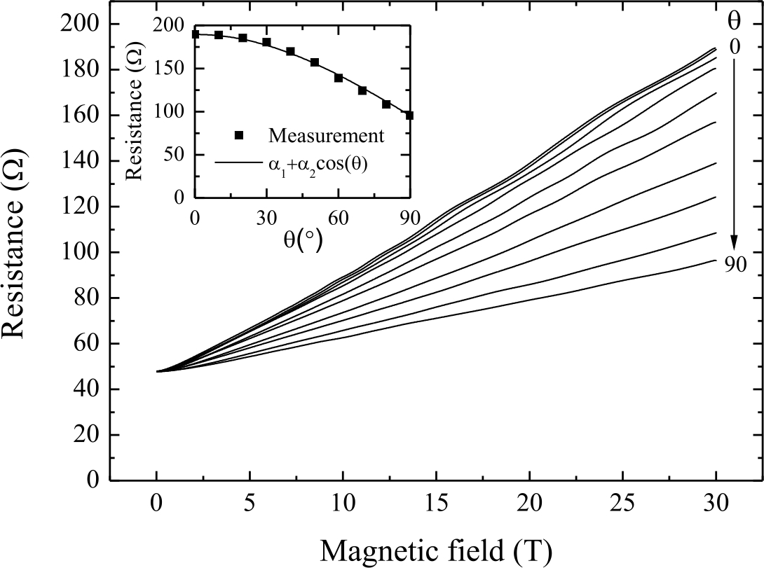
An important observation in the discussion whether 2D effects originate from the bulk or the topological surface is shown in Fig. 4. The dependence of the MR on the applied magnetic field direction suggests 2D behavior (although the MR does not vanish for in plane fields, see also Ref. Qu2010 ). However, from analyzing Hall measurements and Shubnikov de Haas oscillations, it can be shown that the conductance of the bulk of this sample is larger than the conductance from the surface Veldhorst2012a . Therefore, when a large 2D effect is then seen on the scale of the total conductace, it seems unlikely that the LMR in this case originates from the surface states alone.
IV.2 Quantum vs classical effect
Attempts have been made Tang2011 ; He2012 ; Wang2012 to explain the observation of LMR by the quantum magnetoresistance model of Abrikosov. The disappearance of the LMR for ultrathin films indicates a relation to the gapless linear dispersion. The low temperature dependence of the observed LMR also points towards Abrikosov’s model. However, as Abrikosov’s model applies to the extreme quantum limit, it is interesting to note that not all LMR observations He2012 ; Wang2012 coincide with observations of Shubnikov-de Haas oscillations. This could indicate that the systems are far away from the extreme quantum limit or that the bulk transport shunts the quantum oscillations. The carrier density in the topological insulator samples are relatively large and for realistic magnetic field values more than one Landau level is usually occupied. If Abrikosov’s model is used to explain the LMR in these topological insulators, it is important to know up to which filling factor Abrikosov’s model could still apply.
To explain the LMR observed in Bi2Se3 nanosheets Tang2011 , Wang and Lei Wang2012a derive a different model for the LMR using the balance-equation approach Lei1985 . They found that for a 2D system with linear dispersion and a non-zero g factor a LMR can arise. The model shows that the LMR can occur for fields much lower than , it actually requires that the Landau levels overlap. When the mobility decreases, the required field for SdH oscillations increases, whereas the LMR gets even stronger. For higher mobilities, SdH oscillations start to appear and the LMR weakens, because in this regime the overlap of the Landau levels decreases. This also accounts for the low temperature dependence of the LMR, as with higher temperature the Landau levels will broaden, increasing the overlap. It is clear that the system is far away from the extreme quantum limit, in contrast to Abrikosov’s model. By investigating the density dependence of the LMR, the model of Wang and Lei can also be distinguished from Abrikosov’s model. The latter predicts an behavior where , while the former predicts . A positive g factor is required for a positive LMR. The question arises whether Wang and Lei’s model could also explain the strength of the LMR, as some reports indicate that the surface g factor could be quite low Xiong2012a . This model was derived for Bi2Se3 nanosheets Tang2011 , but could deviate for other topological insulator samples. It assumes a linear dispersion, but ARPES measurements have shown that Bi2Te3 deviates from a linear dispersion. The bulk contribution was assumed to be negligible, although in many transport measurements the bulk is still prominent. It would be interesting to see whether the model by Wang and Lei Wang2012a would still be linear when generalized beyond a linear dispersion and in the presence of bulk shunts.
Alternatively, Assaf Assaf2012 used a modified HLN model to explain the observed LMR. Their extended HLN model takes the WAL effect and a classical component into account. In a certain magnetic field range, the logarithmic WAL component cancels the component, leaving a linear MR dependence. According to this model, the quadratic component should be distinguishable from a truly linear MR for higher fields, so it would therefore be interesting to investigate whether this idea is still consistent with measurements at even higher fields.
A number of reports Wang2012 ; Tang2011 ; Gao2012 ; Assaf2012 ; Wang2012 ; Zhang2011 mention that the Parish-Littlewood model also could cause a LMR. Although Assaf Assaf2012 indicate that their samples contain a lot defects, they exclude the possibility that this model explains the LMR, as there is a disagreement between the range of the mobility and the range of the LMR. Others Wang2012 ; Wang2012a also indicate that it is unlikely that the model by Parish and Littlewood explains the observed LMR, as the topological insulator samples have a high quality crystal structure and no structural inhomogeneities are observed. Although Tang Tang2011 also do not expect structural inhomogeneities, they indicate that electronic inhomogeneities cannot be excluded, which has been confirmed by the observation of potential fluctuations in scanning tunneling measurements Beidenkopf2011 . More research is therefore required to investigate whether the model by Parish and Littlewood could apply to these topological insulator samples. Expecting a relatively large size of electrodes or contacts in some of the reported transport experiments it would also be useful to study more mundane explanations of LMR such as a non-homogeneous current injection into an otherwise homogenous sample, whereby a transverse Hall component can easily be picked up Pippard1989 .
V Topological insulators with proximity induced superconductivity
The combination of superconductivity with spin-orbit coupling opens many new exciting research directions, including the realization of a new emergent particle: the Majorana fermion. This particle, which is its own antiparticle, emerges from the electron-hole symmetry of superconducting condensation and the spin-momentum locking in the topological insulator Fu2008 ; Fu2009 . The high potential of this particle in quantum computation led to many new proposals in various material systems, such as topological insulator/superconductor structures Fu2008 ; Fu2009c ; Law2009 , spin-triplet -wave superconductors Kitaev2001 ; Read2000 ; Bolech2007 ; Sengupta2001 ; Kraus2009 , helical superconductors Sato2009c , topological superconductors Sasaki2011 ; Heumen2012 ; Fu2010c ; Hsieh2012b ; Yamakage , semiconductor/metals with strong orbit coupling in combination with superconductors or superconductors with strong spin orbit coupling Sato2010c ; Potter2010 ; Sau2010 ; Alicea2010 . In the latter category the most well-known device is inducing superconductivity in nanowires structures with strong Zeeman and Rashba fields Sau2010 ; Alicea2010 ; Lutchyn2010 ; Oreg2010 ; Klinovaja2012 ; Tewari2011 ; Lutcgyn2011 ; Golub2011 ; Flensberg2010 ; Romito2011 ; Bena2012 ; Potter2011a . First signatures of the Majorana fermion are revealed Lutchyn2010 ; Oreg2010 ; Mourik2012 ; Reich2012 ; Das2012 but in order to test all its peculiar properties the realization of superconducting interference devices will be a prerequisite Alicea2012 ; Beenakker2012 .
V.1 Supercurrents through TI structures
Shortly after the discovery of the Bi-compound topological insulators, observations of supercurrents in superconductor - topological insulator structures have been reported Sacepe2011 ; Veldhorst2012a ; Qu2012 ; Zhang2011 ; Veldhorst2012b ; Williams2012 ; Zareapour2012 , as well as the coexistence of superconductivity and topological surface states Wang20122 . Several fabrication techniques have been used such as epitaxial film growth and mechanical exfoliation for the topological insulator structure. Superconducting electrodes are deposited on top resulting in lateral junctions. Sandwich-type junctions have been realized by Qu Qu2012 using a clever fabrication method based on exfoliated flakes. Using an oxidized Si substrate, Sacépé Sacepe2011 demonstrated gate tunable supercurrents. The change in the product is of the order of 15% by applying a gate voltage between -80 V and +50 V. Structures based on exfoliation are therefore flexible and have high potential. High quality topological insulators with small thicknesses and smooth surfaces can be realized that allow the construction of multiple devices on a single flake Veldhorst2012a .
The characteristic product observed so far is well below the characteristic voltage scale of , e.g. 5 mV for superconducting niobium electrodes. Although mechanisms as scattering and electron-hole decoherence due to junction lengths longer than can lower the product, these junctions often have high interface transparencies and junction lengths comparable to . In these systems, an important mechanism lowering the product is the presence of bulk conduction. Normal state transport is dominated by the bulk states which are spread over the entire sample. As the electrodes are fabricated on top, proximity induced superconductivity will be the strongest on the top, and the bulk is effectively shunting the junction significantly, thereby reducing the product. Veldhorst Veldhorst2012a obtained a bulk mean free path shorter than the junction length while the system is in the ballistic limit and concluded that the discrimination between bulk and surface states can be so strong that the top topological surface state dominates the superconducting transport, while the bulk states dominate the normal state.
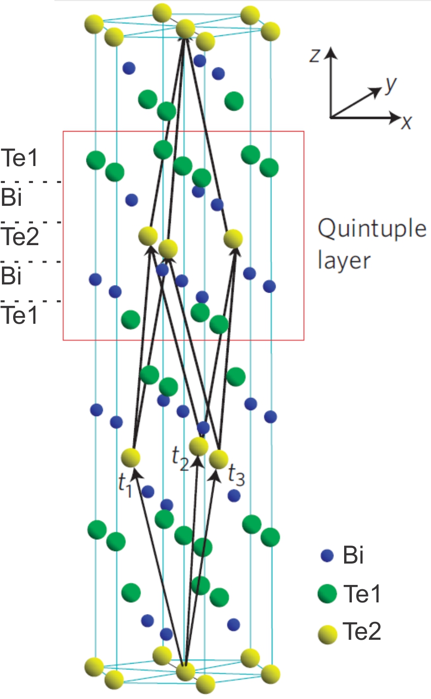
It is an intriguing question why this discrimination is so strong. Besides geometrical effects, strong anisotropy of the band structure of Bi-based topological insulators is a possible origin. The ratio of the superconducting coherence length in the topological insulator depends on the effective mass and the potential energy difference along the -direction and -direction. From the expression of the coherence-length tensor for anisotropic superconductors as described in Ref. Meuth1988 , we find for the proximity coherence length in the non-superconducting material
| (6) |
where the , and axis are as defined in Fig. 1. The superconductivity is induced in the surface states in the plane. and are the lattice constants of the unit cell along the (or ) and direction, respectively. Using the valence band effective masses and for Bi2Te3 Yavorsky2011 in conjunction with the lattice constant differences, we find a ratio of 0.15. Hence, the band structure itself causes a strong anisotropic proximity effect. An additional argument for strong anisotropy is the observation of the layered quantum Hall effect in Bi2Te3 Cao2012 . Furthermore, the effective parameter that determines the suppression of in S-N-S junctions (whether ballistic or diffusive, and including barriers at interfaces) is given by , with the boundary resistance and the interlayer resistance Golubov2004 . From this suppression parameter it can already be seen that a low interlayer resistance with respect to the boundary resistance gives a high . The is then suppressed more strongly for the bulk than for the surface channel. Finally, topological effects might render the interfaces to the surface states intrinsically transparent. These intriguing options open a new exciting research direction and give the opportunity to have surface states dominating the supercurrent in topological insulators even in the presence of substantial bulk conductivity.
Successive Andreev reflections allow quasiparticles to escape from the superconducting gap in the voltage state. These multiple Andreev reflection (MAR) processes cause structures in the current voltage characteristics at voltages , with an integer and for standard Cooper pair tunneling and for single electron tunneling mediated by Majorana fermions. Experimentally, Zhang Zhang2011 have reported evidences for MAR for junctions that are in the standard regime (as expected for 3D junctions). Remarkably, in this experiment only steps are observed for even .
V.2 Current-phase relationship
Topological protection causes interfaces to be highly transparent due to Klein tunneling Fu2008 ; Fu2009 and absence of backscattering for perpendicular incidence. This protection can change the standard current-phase relationship in Josephson junctions from with to .The systems is then gapless at zero energy, and there exist a Majorana bound state when the phase difference across the junction equals . Many theoretical proposals have been put forward to reveal this current-phase relationship. These proposals are based on the and Josephson effects and superconducting quantum interference devices with topological interlayers.
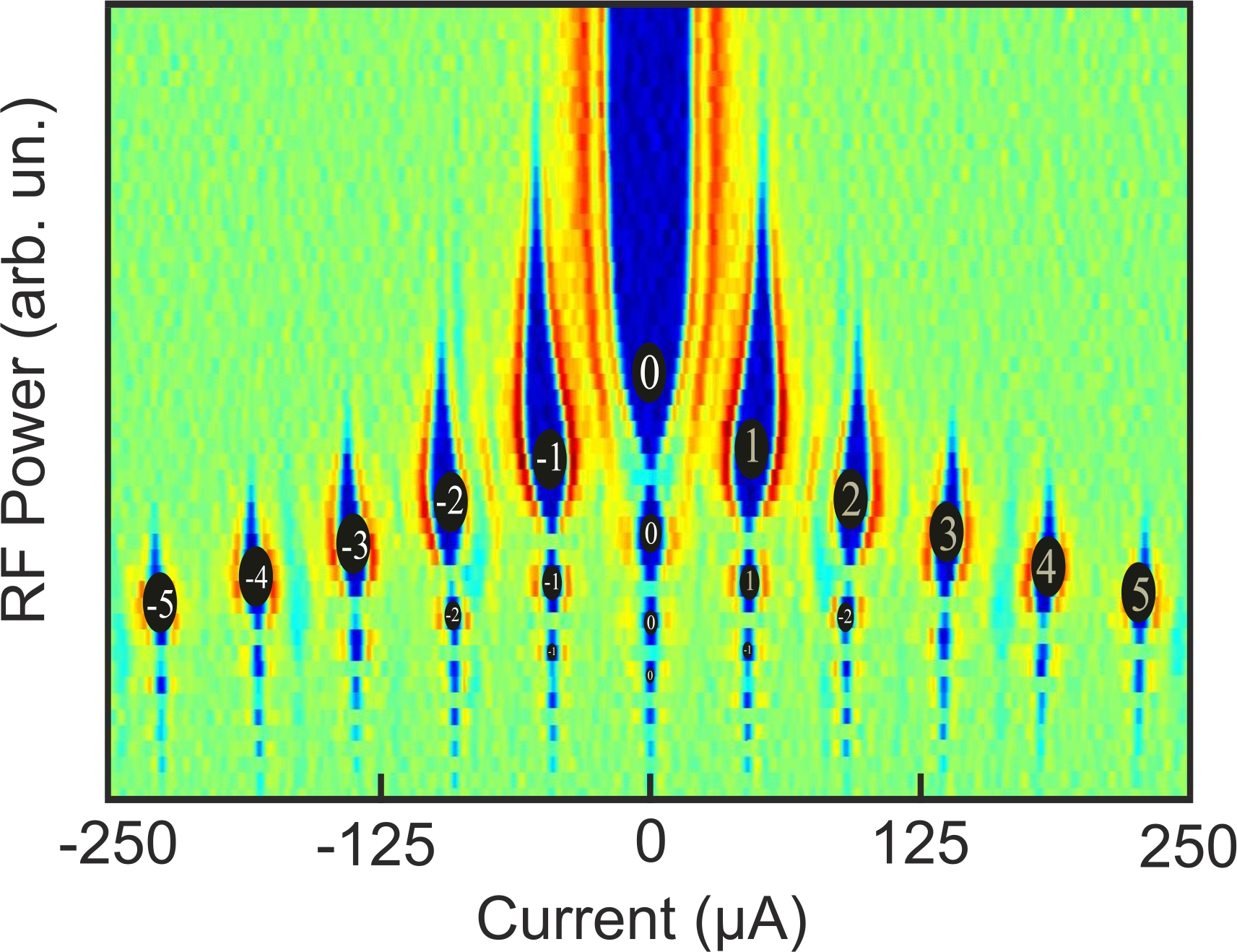
The Josephson effect has been observed by Veldhorst Veldhorst2012a , see Fig. 5. These Josephson junctions show clear steps when irradiated with microwaves, demonstrating the Josephson nature of the supercurrent and from the spacing between the steps it can be concluded that these measurements are in the regime. Future strategies to enhance the fraction of tunneling involve non-equilibrium measurements Badiane2011 and the suppression of non-perpendicular trajectories in the junctions Snelder2012 .
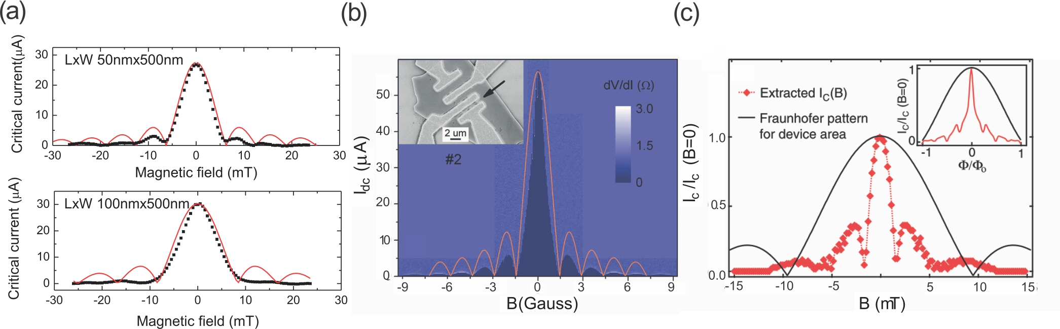
The Josephson effect causes a modulation of the superconducting critical current in an applied magnetic field. In the limit of infinite width and a homogenous current density distribution the magnetic field dependence of the critical current is the Fraunhofer sinc function:
| (7) |
Here, is the superconducting flux quantum. Fig. 6 shows typical critical current modulation patterns observed so far. The Josephson junctions fabricated by Qu Qu2012 are well described by Eq. (7) with , while Veldhorst Veldhorst2012a and Williams Williams2012 report deviations.
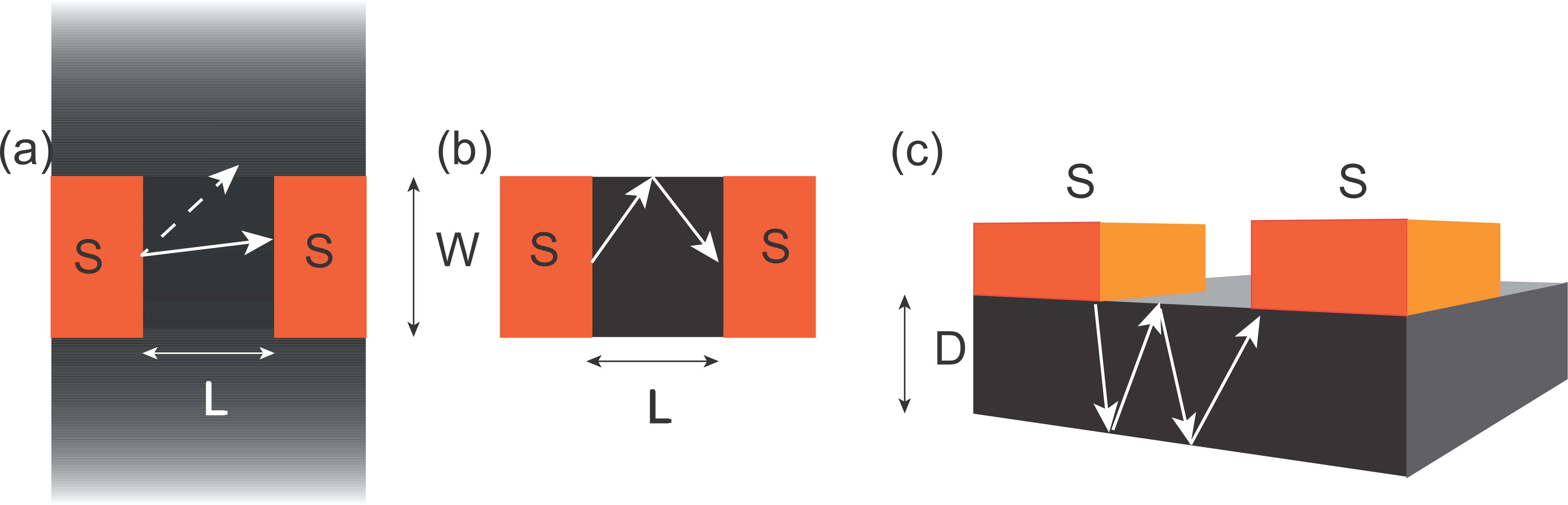
Deviations in the field dependence can result from flux focusing effects and geometrical inhomogeneities, e.g. pinholes result in a slower decay of the side lobes, while lower current densities at the edges result in faster decay of the side lobes. Furthermore, having a finite width changes the field dependence, which becomes significant when , the situation for most experiments so far. The ratio between the length and the width of the junctions can change both the magnitude and period of the diffraction pattern Heida1998 . The period increases from to for Barzykin1999 when the junction edges are ‘open’, as in Fig. 7(a). In this scenario, the side lobes will decrease more rapidly.
When specular reflection occurs at the edge of the junction, such as in Fig. 7(b), the crossover occurs at smaller aspect ratiosLedermann1999 : . The ratio that is important in this scenario is the distance between the Josephson vortex and the range of nonlocal electrodynamics, determined by the thermal length . As long as the range of nonlocal electrodynamics is smaller than the distance between vortices, the period remains. For a larger range or strong nonlocality the period becomes due to boundary effects. Including a finite tunneling barrier to this geometry mainly causes a sharpening of the Fraunhofer pattern and the side lobs are flattened Sheehy2003 . This flattening is also characteristic for SNS junctions in the diffusive limit Bergeret2008 . A third situation occurs when the magnetic field is parallel to the surface but perpendicular to the current as shown in Fig. 7(c). This changes the Fraunhofer pattern drastically Mohammadkhani2008 , including irregular periods, periods smaller than the flux quantum and non-zero minima depending on the ratio. The experimentally realized dc SQUIDs by Veldhorst Veldhorst2012b based on junctions where the critical current field dependency deviates from the standard Fraunhofer pattern Veldhorst2012a show standard fluxoid quantization and suggest that the junction deviations are due to geometrical effects.
The observation of Fraunhofer patterns in topological Josephson junctions unambiguously shows the development of the superconducting proximity effect in the topological insulator. The deviations from the standard Fraunhofer form an interesting platform to search for new phenomena in these junctions. However, these junctions are nanosized, are often ballistic, and multiple bands can contribute to the conduction, resulting in complex scenarios. Still, based on these Josephson junctions SQUIDs can be fabricated that can discriminate between geometrical effects and transport mediated by Majorana fermions.
V.3 dc SQUIDs with unconventional current phase relationships
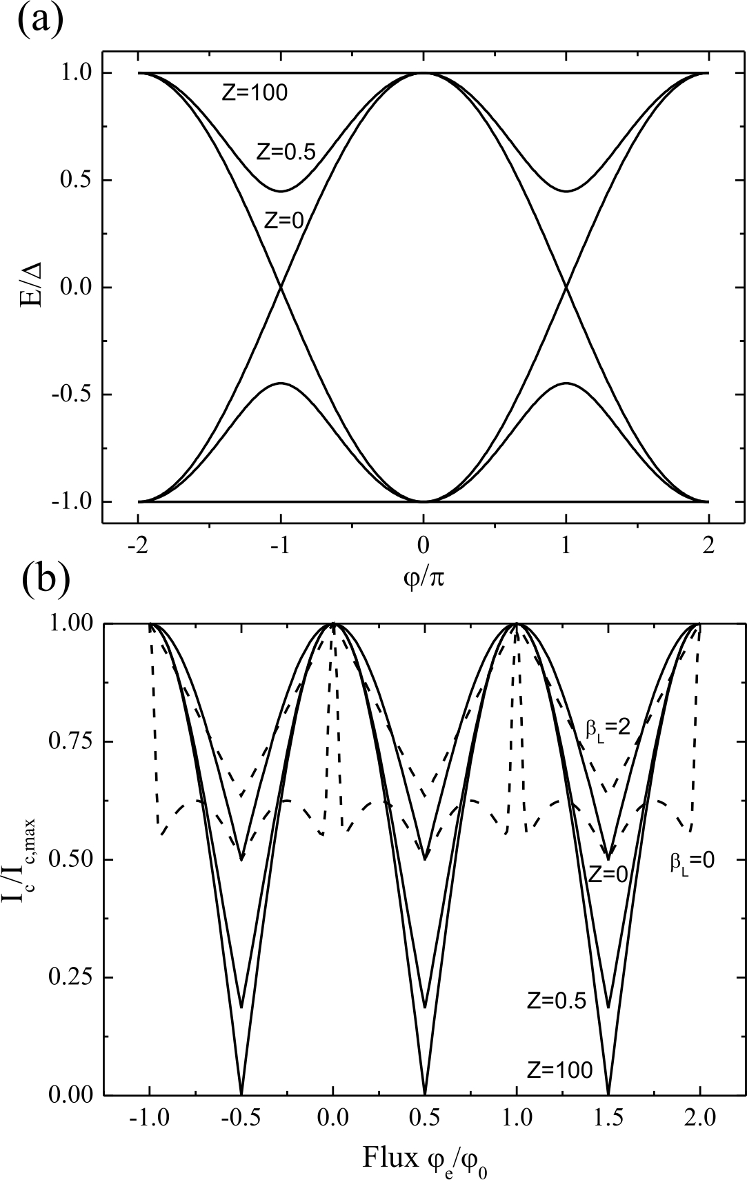
Due to the appearance of Majorana fermions single electron tunneling occurs and the resulting current-phase relation of Josephson junctions can become -periodic. The -periodic current-phase relationship of topological Josephson junctions has its signatures in superconducting loops Heck2011 . In the absence of relaxation mechanisms, standard fluxoid quantization is doubled. Unfortunately, mechanisms such as quasiparticle poisoning and quantum phase slips will drive the system easily to standard fluxoid quantization. However, as shown by Veldhorst Veldhorst2012c , even in this regime the unusual current phase relation of the individual junctions alter the standard SQUID modulation characteristics. This model is based on imposing fluxoid quantization on a superconducting loop interrupted by two Josephson junctions described with the resistivily and capacitively shunted junction (RCSJ) model. To further illustrate this model we show the scenario of full relaxation in Fig. 8, where the junctions have been modeled by the Blonder-Tinkham-Klapwijk (BTK) approach Blonder1982 . The resulting bound states are described by . Here, is the BTK barrier strength of the barriers . These results also represent bound states of superconductor - topological insulator Josephson junctions, where the factor effectively describes the scattering resulting from finite angle incidence with momentum mismatches and the appearance of a magnetic gap. In the standard SQUID scenario, the Josephson junctions have low transparency (corresponding to in Fig. 8) and can be described with a current-phase relationship. In that case the dc SQUID has a sinusoidal critical current modulation as a function of magnetic field and standard fluxoid quantization . Lowering the barrier strength, increasing the interface transparency, results in an incomplete critical current modulation Veldhorst2012c . This incomplete modulation is a strong signature, since it is independent on the junction homogeneity and survives up to the regime of energy relaxation (where doubled fluxoid quantization is absent Fu2009 ).
We also included the current-phase relationship as imposed phenomenologically by Williams Williams2012 . This model assumes a current-phase relation that peaks when the relative phase over the junction equals . In the regime of small self-induced flux, described by the screening parameter , the characteristic spikes are also present in the dc SQUID characteristics. Increasing smears out the spikes, resulting in a triangular critical current modulation, see Fig. 8. We conclude this section by noting that dc SQUIDs are ideal candidates to measure the unusual current-phase relationships of superconductor-topological insulator structures even in the presence of junction inhomogeneities and relaxation mechanisms. These dc SQUIDs can be used to test whether the critical current field dependences of topological junctions are due to intrinsic or extrinsic effects.
This work is supported by the Netherlands Organization for Scientific Research (NWO) through VIDI and VICI grants, and by the Dutch Foundation for Fundamental Research on Matter (FOM).
References
- (1) L. Fu, C. L. Kane, and E. J. Mele, Phys. Rev. Lett 98(10), 106803 (2007).
- (2) L. Fu and C. L. Kane, Phys. Rev. B 76(4), 045302 (2007).
- (3) H. Zhang et al., Nat. Phys. 5, 438 (2009).
- (4) T. Sato et al., Phys. Rev. Lett. 105, 136802 (2010).
- (5) K. Kuroda et al., Phys. Rev. Lett. 105, 146801 (2010).
- (6) Y. L. Chen et al., Phys. Rev. Lett. 105, 266401 (2010).
- (7) S. Souma et al., Phys. Rev. Lett. 108, 116801 (2012).
- (8) K. Kuroda et al., Phys. Rev. Lett. 108, 206803 (2012).
- (9) S.-Y. Xu et al., arXiv:1007.5111 (unpublished).
- (10) Z. Ren, A. A. Taskin, S. Sasaki, K. Segawa, Y. Ando, Phys. Rev. B 82, 241306 (2010).
- (11) J. Xiong, A. C. Petersen, D. Qu, Y.S. Hor, R. J. Cava, N.P. Ong, Physica E 44, 917 (2012).
- (12) Z. Ren, A. A. Taskin, S. Sasaki, K. Segawa, Y. Ando, Phys. Rev. B 84, 165311 (2011).
- (13) A. Y. Kitaev, Phys. -Usp. 44 131 (2001).
- (14) L. Fu, C.L. Kane, Phys. Rev. Lett. 100, 096407 (2008).
- (15) S. Sasaki et al., Phys. Rev. Lett. 107, 217001 (2011).
- (16) E. van Heumen et al., arXiv: 1110.4406 (2012).
- (17) Y. S. Kim, M. Brahlek, N. Bansal, E. Edrey, G. A. Kapilevich, K. Iida, M. Tanimura, Y. Horibe, S. W. Cheong, and S. Oh, Phys. Rev. B 84(7), 073109 (2011).
- (18) M. Liu, C. Z. Chang, Z. Zhang, Y. Zhang, W. Ruan, K. He, L. l. Wang, X. Chen, J. F. Jia, S. C. Zhang, Q. K. Xue, X. Ma, and Y. Wang, Phys. Rev. B 83(16), 165440 (2011).
- (19) S. Hikami, A. Larkin, and Y. Nagaoka, Prog. Theor. Phys. 63(2), 707–710 (1980).
- (20) H. T. He, G. Wang, T. Zhang, I. K. Sou, G. K. L. Wong, J. N. Wang, H. Z. Lu, S. Q. Shen, and F. C. Zhang, Phys. Rev. Lett. 106(16), 166805 (2011).
- (21) G. Zhang, H. Qin, J. Chen, X. He, L. Lu, Y. Li, and K. Wu, Adv. Funct. Mater. 21(12), 2351–2355 (2011).
- (22) H. Steinberg, J.B. Lal e, V. Fatemi, J.S. Moodera, and P. Jarillo-Herrero, Phys. Rev. B 84(23), 233101 (2011).
- (23) J. G. Checkelsky, Y. S. Hor, R. J. Cava, and N. P. Ong, Phys. Rev. Lett. 106(19), 196801 (2011).
- (24) J. J. Cha, M. Claassen, D. Kong, S. S. Hong, K. J. Koski, X. L. Qi, and Y. Cui, Nano Lett. 12(8), 4355–4359 (2012).
- (25) S. Iordanskii, Y. Lyanda-Geller, and G. Pikus, JETP Letters 60(3), 206 (1994).
- (26) F. E. Meijer, A. F. Morpurgo, T. M. Klapwijk, and J. Nitta, Phys. Rev. Lett. 94(18), 186805 (2005).
- (27) J. Wang, A. M. DaSilva, C. Z. Chang, K. He, J. K. Jain, N. Samarth, X. C. Ma, Q. K. Xue, and M. H. W. Chan, Phys. Rev. B 83(24), 245438 (2011).
- (28) Y. Takagaki, B. Jenichen, U. Jahn, M. Ramsteiner, and K. J. Friedland, Phys. Rev. B 85(11), 115314 (2012).
- (29) S. Zhang, L. Yan, J. Qi, M. Zhuo, Y. Q. Wang, R. Prasankumar, Q. Jia, and S. Picraux, Thin Solid Films 520(21), 6459–6462 (2012).
- (30) J. Chen, H. J. Qin, F. Yang, J. Liu, T. Guan, F. M. Qu, G. H. Zhang, J. R. Shi, X. C. Xie, C. L. Yang, K. H. Wu, Y. Q. Li, and L. Lu, Phys. Rev. Lett. 105(17), 176602 (2010).
- (31) J. Chen, X. Y. He, K. H. Wu, Z. Q. Ji, L. Lu, J. R. Shi, J. H. Smet, and Y. Q. Li, Phys. Rev. B 83(24), 241304 (2011).
- (32) A. A. Taskin, S. Sasaki, K. Segawa, and Y. Ando, Phys. Rev. Lett. 109(6), 066803 (2012).
- (33) B.F. Gao, P.Gehring, M. Burghard, and K. Kern, Appl. Phys. Lett. 100, 212402 (2012).
- (34) H. B. Zhang, H. L. Yu, D. H. Bao, S. W. Li, C. X. Wang, and G. W. Yang, Phys. Rev. B 86(7), 075102 (2012).
- (35) H. Z. Lu and S. Q. Shen, Phys. Rev. B 84(12), 125138 (2011).
- (36) I. Garate and L. Glazman, Phys. Rev. B 86(3), 035422 (2012).
- (37) H. Steinberg, D. R. Gardner, Y. S. Lee, and P. Jarillo-Herrero, Nano Lett. 10(12), 5032–5036 (2010).
- (38) H. Z. Lu, J. Shi, and S. Q. Shen, Phys. Rev. Lett. 107(7), 076801 (2011).
- (39) J. J. Cha, D. Kong, S. S. Hong, J. G. Analytis, K. Lai, and Y. Cui, Nano Lett. 12(2), 1107–1111 (2012).
- (40) M. Liu, J. Zhang, C. Z. Chang, Z. Zhang, X. Feng, K. Li, K. He, L. l. Wang, X. Chen, X. Dai, Z. Fang, Q. K. Xue, X. Ma, and Y. Wang, Phys. Rev. Lett. 108(3), 036805 (2012).
- (41) Y. Zhang, K. He, C. Z. Chang, C. L. Song, L. L. Wang, X. Chen, J. F. Jia, Z. Fang, X. Dai, W. Y. Shan, S. Q. Shen, Q. Niu, X. L. Qi, S. C. Zhang, X. C. Ma, and Q. K. Xue, Nat Phys 6(8), 584–588 (2010).
- (42) Q. Liu, C. X. Liu, C. Xu, X. L. Qi, and S. C. Zhang, Phys. Rev. Lett. 102(15), 156603 (2009).
- (43) Y. L. Chen, J. H. Chu, J. G. Analytis, Z. K. Liu, K. Igarashi, H. H. Kuo, X. L. Qi, S. K. Mo, R. G. Moore, D. H. Lu, M. Hashimoto, T. Sasagawa, S. C. Zhang, I. R. Fisher, Z. Hussain, and Z. X. Shen, Science 329(5992), 659–662 (2010).
- (44) G. Bergmann, Physics Reports 107(1), 1–58 (1984).
- (45) B. Altshuler and A. Aronov, Solid State Communications 30(3), 115–117 (1979).
- (46) P. A. Lee and T. V. Ramakrishnan, Rev. Mod. Phys. 57(2), 287–337 (1985).
- (47) J. G. Checkelsky, Y. S. Hor, M. H. Liu, D. X. Qu, R. J. Cava, and N. P. Ong, Phys. Rev. Lett. 103(24), 246601 (2009).
- (48) D.E. Beutler and N. Giordano, Phys. Rev. B 38, 8 (1988).
- (49) J.J. Lin and N. Giordano, Phys Rev. B 35, 545 (1987).
- (50) J. G. Analytis, J. H. Chu, Y. Chen, F. Corredor, R. D. McDonald, Z. X. Shen, and I. R. Fisher, Phys. Rev. B 81(20), 205407 (2010).
- (51) J. Xiong, Y. Luo, Y. Khoo, S. Jia, R. J. Cava, and N. P. Ong, Phys. Rev. B 86(4), 045314 (2012).
- (52) D.-X. Qu, Y. S. Hor, J. Xiong, R.J. Cava, and N.P. Ong, Science 329, 821 (2010).
- (53) A.A. Taskin, K. Segawa, and Y. Ando, Phys. Rev. B 82, 121302 (2010).
- (54) J.G. Analytis, R.D. McDonald, S.C. Riggs, J.-H. Chu, G.S. Boebinger, and I.R. Fisher, Nature Phys. 10, 960 (2010).
- (55) B. Sacépé, J.B. Oostinga, J. Li, A. Ubaldini, N.J.G. Couto, E. Giannini, and A.F. Morpurgo, Nature Commun. 2, 575 (2011).
- (56) C. Brüne, C.X. Liu, E.G. Novik, E.M. Hankiewicz, H. Buhmann, Y.L. Chen,X. L.Qi, Z.X. Shen, S. C. Zhang, and L.W. Molenkamp, Phys. Rev. Lett. 106, 126803 (2011).
- (57) F. Xiu, L. He, Y. Wang, L. Cheng, L.-T. Chang, M. Lang, G. Huang, X. Kou, Y. Zhou, X. Jiang, Z. Chen, J. Zou, A. Shailos, and K.L. Wang, Nature Nano. 6, 216 (2011).
- (58) A.A. Taskin, Z. Ren, S. Sasaki, K. Segawa, Y. Ando, Phys. Rev. Lett. 107, 016801 (2011).
- (59) J. Xiong, A.C. Petersen, D.-X. Qu, Y.S. Hor, R.J. Cava, and N.P. Ong, Phys. E 44, 917 (2012).
- (60) M. Veldhorst, M. Snelder, M. Hoek, T. Gang, V.K. Guduru, X.L. Wang, U. Zeitler, W.G. van der Wiel, A.A. Golubov, H. Hilgenkamp, and A. Brinkman, Nature Mater. 11, 417 (2012).
- (61) H. Cao, J. Tian, I. Miotkowski, T. Shen, J. Hu, S. Qiao, and Y.P. Chen, Phys. Rev. Lett. 108, 216803 (2012).
- (62) Z. Ren, A.A. Taskin, S. Sasaki, K. Segawa, and Y. Ando, Phys. Rev. B 84, 075316 (2011).
- (63) Z. Ren, A.A. Taskin, S. Sasaki, K. Segawa, and Y. Ando, Phys. Rev. B 85, 155301 (2012).
- (64) I.M. Lifshitz and A.M. Kosevich, Sov. Phys. JETP 2, 636 (1956).
- (65) K.S. Novoselov, A.K. Geim, S.V. Morozov, D. Jiang, M.I. Katsnelson, I.V. Grigorieva, S.V. Dubonos, A.A. Firsov, Nature 438, 197 (2005).
- (66) Y. Zhang, Y.-W. Tan, H.L. Stormer, P. Kim, Nature 438, 201 (2005).
- (67) G.P. Mikitik and Yu.V. Sharlai, Phys. Rev. B 85, 033301 (2012).
- (68) A.A. Taskin and Y. Ando, Phys. Rev. B 84, 035301 (2011).
- (69) X. Wang, Y. Du, S. Dou, and C. Zhang, Phys. Rev. Lett. 108, 266806 (2012).
- (70) H. Tang, D. Liang, R.L.J. Qiu, and X.P.A. Gao, ACS Nano 5, 7510 (2011).
- (71) H. He, B. Li, H. Liu, X. Guo, Z. Wang, M. Xie, and J. Wang, Appl. Phys. Lett. 100, 032105 (2012).
- (72) B.A. Assaf, T. Cardinal, P. Wei, F. Katmis, J.S. Moodera, and D. Heiman, arXiv:1205.4635 (2012).
- (73) P. Kapitza, Proc. R. Soc. London, Ser. A 119, 358 (1928).
- (74) A.A. Abrikosov, Europhys. Lett. 49, 789 (2000).
- (75) A.A. Abrikosov, Sov. Phys. JETP 29, 746 (1969).
- (76) A.A. Abrikosov, Phys. Rev. B 58, 2788 (1998).
- (77) J. Hu and T.F. Rosenbaum, Nature Materials 7, 697 (2008).
- (78) K. Eto, A.A. Taskin, K. Segawa, and Y. Ando, Phys. Rev. B 81, 161202(R) 2010.
- (79) R. Xu et al., Nature 390, 57 (1997).
- (80) W. Zhang et al., Phys. Rev. Lett. 106, 156808 (2011).
- (81) M.M. Parish and P.B. Littlewood, Nature 426, 162 (2003).
- (82) M.M. Parish and P.B. Littlewood, Phys. Rev. B 72, 094417 (2005).
- (83) C.M. Wang and X.L. Lei, Phys. Rev. B 86, 035442 (2012).
- (84) X.L. Lei and C.S. Ting, Phys. Rev. B 30, 4809 (1984); 32, 1112 (1985).
- (85) H. Beidenkopf et al., Nature Phys. 7, 939 (2011).
- (86) A.B. Pippard, Magnetoresistance in Metals, Cambridge Studies in Low Temperature Physics, 1989.
- (87) L. Fu, and C.L. Kane, Phys. Rev. B 79 161408(R) (2009).
- (88) L. Fu and C. L. Kane, Phys. Rev. Lett. 102, 216403 (2009); A. R. Akhmerov, J. Nilsson, C. W. J. Beenakker, Phys. Rev. Lett. 102, 216404 (2009); Y. Tanaka, T. Yokoyama, and N. Nagaosa, Phys. Rev. Lett. 103, 107002 (2009); J. Linder, Y. Tanaka, T. Yokoyama, A. Sudbo, N. Nagaosa, Phys. Rev. Lett. 104, 067001 (2010).
- (89) K. T. Law, P. A. Lee, and T. K. Ng, Phys. Rev. Lett. 103, 237001 (2009).
- (90) N. Read, D. Green, Phys. Rev. B 61, 10267 (2000).
- (91) C. J. Bolech, E. Demler, Phys. Rev. Lett. 98, 237002 (2007).
- (92) K. Sengupta et al., Phys. Rev. B 63, 144531 (2001).
- (93) Y. E. Kraus, A. Auerbach, H. A. Fertig, S. H. Simon, Phys. Rev. B 79, 134515 (2009).
- (94) M. Sato, S. Fujimoto, Phys. Rev. B 79, 094504 (2009); Y. Tanaka, T. Yokoyama, A. V. Balatsky, N. Nagaosa, Phys. Rev. B 79, 060505 (2009).
- (95) L. Fu, E. Berg, Phys. Rev. Lett. 105, 097001 (2010).
- (96) T. H. Hsieh, L. Fu, Phys. Rev. Lett. 108, 107005 (2012).
- (97) A. Yamakage, K. Yada, M. Sato, Y. Tanaka, Phys. Rev. B 85, 180509 (2012).
- (98) M. Sato. Y. Takahashi, S. Fujimoto, Phys. Rev. Lett. 103, 020401 (2009); M. Sato,Y. Takahashi, S. Fujimoto, Phys. Rev. B 82, 134521 (2010).
- (99) A. C. Potter, P.A. Lee, Phys. REv. Lett. 105, 227003 (2010); J. Linder, A. Sudbo, Phys. Rev. B 82, 08314 (2010); A. Yamakage, Y. Tanaka, N. Nagaosa, Phys. Rev. Lett. 108, 087003 (2012).
- (100) J.D. Sau, R.M. Lutchyn, S. Tewari, S. Das Sarma, Phys. Rev. Lett. 104, 040502 (2010); T.D. Stanescu, J. D. Sau, R. M. Lutchyn, S. Das. Sarma, Phys. Rev. B 81, 241310 (2010).
- (101) J. Alicea, Phys. Rev. B 81, 125318 (2010).
- (102) R.M. Lutchyn, J. D. Sau, S. Das Sarma, Phys. Rev. Lett. 105, 077001 (2010); J. D. Sau, S. Tewari, R. M. Lutchyn, T. D. Stanescu, S. Das Sarma, Phys. Rev. B 82, 214509 (2010).
- (103) Y. Oreg, G. Refael, F. von Oppen, Phys. Rev. Lett. 105, 214509 (2010).
- (104) J. Klinovaja, D. Loss, Phys. Rev. B 86, 085408 (2012).
- (105) S. Tewari, T. D. Stanescu, J. D. Sau, S. Das Sarma, New Journal of Physics 13, 065004 (2011); J. D. Sau,S. Tewari, S. Das Sarma, arXiv:1111.2054; T. D. Stanescu, R. M. Lutchyn, S. Das Sarma, Phys. Rev. B 84, 144522 (2011).
- (106) R. M. Lutchyn, T. D. Stanescu, S. Das Sarma, Phys. Rev. Lett. 106, 127001 (2011); R. M. Lutchyn, M. P. A. Fisher, Phys. Rev. B 84, 214528 (2011).
- (107) A. Golub, I. Kuzmenko, and Y. Avishai, Phys. Rev. Lett. 107, 176802 (2011).
- (108) K. Flensberg, Phys. Rev. B 82, 180516 (2010).
- (109) A. Romito, J. Alicea, G. Refael,F. von Oppen, arXiv:1110.6193 (2011); J. Alicea, arXiv:1202.1293.
- (110) C. Bena, D. Sticlet, and P. Simon, Phys. Rev. Lett. 108, 096802 (2012).
- (111) A. C. Potter and P. A. Lee, Phys. Rev. B 83, 094525 (2011); B. Zhou, S.-Q. Shen, Phys. Rev. B 84, 054532 (2011); K. T. Law and P. A. Lee, Phys. Rev. B 84,081304 (2011).
- (112) V. Mourik, K. Zuo, S.M. Frolov, S.R. Plissard, E.P.A.M. Bakkers, and L.P. Kouwenhoven, Science 25, 336 (2012).
- (113) E. S. Reich, Nature News 483, 132 (2012); F. Wilczek, Nature 486, 195 (2012).
- (114) A. Das, Y. Ronen, Y. Most, Y. Oreg, M. Heiblum, H. Shtrikman, arXiv:1205.7073; L. P. Rokhinson, X. Liu, J. K. Furdyna, arXiv:1204.4212; M. T. Deng, C. L. Yu, G. Y. Huang, M. Larsson, P. Caroff, H. Q. Xu, arXiv:1204.4130.
- (115) J. Alicea, Rep. Prog. Phys. 75, 076501 (2012).
- (116) C.W.J. Beenakker, arXiv: 1112.1950v2.
- (117) F. Qu, F. Yang, J. Shen, Y. Ding, J. Chen, Z. Ji, G. Liu, J. Fan, X. Jing, C. Yang, L. Lu, Sci Rep., 2: 339 (2012).
- (118) D. Zhang, J. Wang, A. M. DaSilva, J. S. Lee, H. R. Gutierrez, M. H. W. Chan, J. Jain, N. Samarth, PRB 84, 165120 (2011).
- (119) M. Veldhorst, C. G. Molenaar, X. L. Wang, H. Hilgenkamp, A. Brinkman, Appl. Phys. Lett. 100, 072602 (2012)
- (120) J. R. Williams, A. J. Bestwick, P. Gallagher, S. S. Hong, Y. Cui, A. S. Bleich, A. S. Bleich, J. G. Analytis, I. R. Fisher, D. Goldhaber-Gordon, PRL 109, 056803 (2012).
- (121) P. Zareapour et al., Nature Communications 3,1056 (2012).
- (122) M.X. Wang, C. Liu, J.P. Xu, F. Yang, L. Miao, M.Y. Yao, C.L. Gao, C. Shen, X. Ma, X. chen, Z.A. Xu, Y. Liu, S.C. Zhang, D. Qian, J.F. Jia, and Q.K. Xue, Science 336, 52 (2012).
- (123) H. Meuth, Phys. Rev. B 38 (1988).
- (124) B. Y. Yavorsky, N. F. Hinsche, I. Mertig, P. Zahn, Phys. Rev. B 84, 165208 (2011).
- (125) A.A. Golubov, M.Yu. Kupriyanov, and E. IL’ichev, Rev. Mod Phys. 76, 411 (2004).
- (126) D.M. Badiane, M. Houzet, and J.S. Meyer, Phys. Rev. Lett. 107, 177002 (2011).
- (127) M. Snelder, M. Veldhorst, A.A. Golubov, A. Brinkman, submitted for publication (2012).
- (128) J. P. Heida, B. J. van Wees, T. M. Klapwijk, G. Borghs, Phys. Rev. B 57, 9995 (1998).
- (129) V. Barzykin, A. M. Zagoskin, Superlat. Microstruct. 25, 797 ”807 (1999).
- (130) U. Ledermann, A. L. Fauchère, G. Blatter, Phys. Rev. B 59, R9027 (1999).
- (131) D. E. Sheehy, A. M. Zagoskin, Phys. Rev. B 68, 144514 (2003).
- (132) F.S. Bergeret, J.C. Cuevas, J Low Temp Phys 153, 304 (2008).
- (133) G. Mohammadkhani, M. Zareyan, Y. M. Blanter, Phys. Rev. B 77, 014520 (2008).
- (134) B. van Heck, F. Hassler, A.R. Akhmerov, and C.W.J. Beenakker, Phys. Rev. B 84, 180502(R) (2011).
- (135) M. Veldhorst, C. G. Molenaar, C. J. M. Verwijs, H. Hilgenkamp, A. Brinkman, Phys. Rev. B 86, 024509 (2012).
- (136) G.E. Blonder, M. Tinkham, T.M. Klapwijk, Phys. Rev. B 25, 4515 (1982).