Resonant and non-dissipative tunneling
in independently contacted graphene structures
Abstract
The tunneling current between independently contacted graphene sheets separated by boron nitride insulator is calculated. Both dissipative tunneling transitions, with momentum transfer due to disorder scattering, and non-dissipative regime of tunneling, which appears due to intersection of electron and hole branches of energy spectrum, are described. Dependencies of tunneling current on concentrations in top and bottom graphene layers, which are governed by the voltages applied through independent contacts and gates, are considered for the back- and double-gated structures. The current-voltage characteristics of the back-gated structure are in agreement with the recent experiment [Science 335, 947 (2012)]. For the double-gated structures, the resonant dissipative tunneling causes a ten times enhancement of response which is important for transistor applications.
pacs:
72.80.Vp, 73.40.Gk, 85.30.MnI Introduction
In contrast to the tunneling processes between bulk materials, 1 the tunneling between low-dimensional systems must be assisted by scattering in order to satisfy the momentum and energy conservation laws, see results and discussions for double quantum wells or wires in Refs. 2 or 3, respectively. When the splitting energy between 2D states (this energy is determined by transverse voltages applied across structure) exceeds the collision broadening energy ( is the departure time), the tunneling probability appears to be proportional . In conditions of tunneling resonanse, when ,this probability is proportional to , 4 i.e. the tunnel current depends on the scattering time in the same way as the current in metallic conductor. The breakdown of the dissipative tunneling regime is possible if the energy spectrum branches are intersected and the energy-momentum conservation laws are satisfied without scattering. For example, the intersection of the parabolic electron branches in double quantum wells takes place if the magnetic field is applied perpendicular to the tunneling direction, see 5 and 6 for the experimental data and theory. Similar intersection between the linear branches of gapless energy spectra should take place in graphene/boron nitride/graphene (G/BN/G) heterostructure. Such a structure was reported recently 7 and the tunneling transistor, which is based on the independently-contacted G-sheets connected through a few monolayer BN, was demonstrated. 8 In contrast to the semiconductor heterostructure case, the independently-contacted G/BN/G structures can be easily realized with the use of the single-layer-transfer technology. 9 But a complete theoretical investigation of tunneling current in such a structure is not performed yet (some numerical results on the tunneling conductance were reported recently 9a but the current-voltage characteristics were not analyzed) and a problem is timely now.
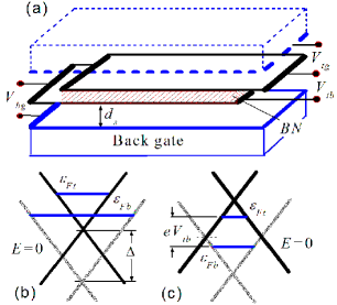
In the paper, we calculate the tunneling current between the independently-contacted top (Gt) and bottom (Gb) graphene layers separated by BN. We analyze the dependencies of on the sheet concentrations (Fermi energies) and on , which are determined by the gate voltages applied to the contacts, see Fig. 1a. Depending on voltages applied, one can realized either electron-electron (hole-hole) or electron-hole regimes of tunneling, as it is shown in Figs. 1b and 1c, respectively. In the latter case the cross-point is located between the Fermi energies ( or vise versa) and the non-dissipative regime of tunneling takes place in addition to the resonant dissipative tunneling transitions. The current-voltage characteristics appears to be different for these regimes. For the back-gated structure, the results are in agreement with the experimental data. 8 For double-gated structures, the resonant dissipative tunneling regime can be realized, with a ten times enhancement of response.
The paper is organized as follows. In Sec. II, we present the basic equations which describe the two regimes of interlayer tunneling. In Sec. III we analyze the current-voltage characteristics and compare the results for the back-gated structure with the of experimental data. 8 The last section includes the discussion approximations used, and the conclusions. In Appendix, we evaluate the effective tunneling Hamiltonian for G/BN/G structure.
II Basic equations
Under consideration of Gt/BN/Gb structure, we use the tunneling Hamiltonian which connects Gt and Gb layers described by 2 matrices , i.e. we introduce 4 matrix 10
| (1) |
Here we have separated the Hamiltonian of uncoupled layers, , and the tunneling contribution, , written through the 2 matrix which is determined by a stacking geometry of the structure, see Appendix. The charge density in Gt and Gb layers, (here and below ), and the tunnel current density, , are determine through the 4 density matrix by the formulas 11
| (2) |
Here is the normalization area, is the projection operator on the -states, and the interlayer current operator is determined from the charge conservation requirement (see similar calculations in Refs. 6), so that
| (3) |
As a result, tunneling processes are described by the above-introduced matrices and , as well as the density matrix governed by the standard equation: . 11
Further, we separate the diagonal and non-diagonal parts of the density matrix which describe the distribution of carriers in Gt- and Gb-layers and the tunneling current, , respectively. Similarly to Ref. 6, one express through the carrier distributions determined by and the tunneling current density takes form
| (4) |
Here means both summations over states of carriers in Gt- and Gb-layers and averaging over lateral disorder which should be included in the Hamiltonians . Calculations of are performed below with the use of the basis formed by 2-row wave functions in th layer determined by the eigenvalue problem . We introduce the spectral density matrix, labeled by 1 and 2, as
| (5) |
where the averaging over random disorder in th layer is performed. Using the Fermi distribution for heavily-doped layers, when is replaced by the -function with the Fermi energies in Eq.(4), we transform into
| (6) | |||
where means summation over the matrix variable.
Below, we express in the momentum representation as , where is the retarded Green’s function of th layer with the cross point energies written through the level-splitting energy. Within the model of short-range disorder with the same statistically independent characteristics for and , the Green’s function in the Born approximation takes form 12
| (7) |
where and are correspondent to - and -layers and cm/s is the carrier velocity. The projection operators on the conduction () and valence () band states, , are written through the 22 isospin Pauli matrix . The self-energy contributions are written through the logarithmically-divergent real correction which is proportional to and the coupling constant . This approach corresponds to the short-range scattering with the cut-off energy . 13 The interlayer tunneling is described by the parameters
| (8) |
which appear under calculation of the matrix trace in Eq. (6). Using Eqs. (7) and (8) we transform the tunneling current density (6) into the form
| (9) |
where the explicit expressions for and are determined by Eq. (7). Due to the in-plane symmetry of the problem, is written as the double-integral over the -plane and the energy interval .
Integrations in (9) are performed analytically for the collisionless case, , and the tunneling current density is given by the sum of the dissipative current, which is and the non-dissipative contribution ():
| (13) | |||
Here the resonant dissipative contribution (at ) is written through the -like function with the phenomenological broadening . At , the non-dissipative contribution is written through the factor ( because ) determined by the tunneling energies and . These parameters depend on the stacking order of the Gt/BN/Gb structure and rough estimate for the case of -layer BN barrier 14 is determined by Eq. (A.4), see Appendix. As a result, we obtain , where 0.4 eV is the interlayer overlap integral and 2.5 eV is of the order of the - and -band energies in BN. We use below 13 eV for and 6 eV for 6-layer BN barrier, which are in agreement with the experimental data of Ref. 8. The scattering parameters used in Eqs. (9, 10) are taken from the conductivity measurements, see similar considerations in Refs. 16. We choose the cut-off energy 0.2 eV and the coupling constants 0.3 or 0.15 corresponded to the maximal sheet resistance 4 or 2 k per square.
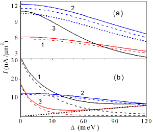
The current density is dependent on , and , which are determined by the drops of voltages applied to three- or four-terminal structures, see Fig. 1a. Before study of the current-voltage characteristics, we consider the dependencies of the total current on these three energies. In Fig. 2 we plot the tunneling current, which is determined by Eqs. (9) and (7), versus for different Fermi energies determined by and at 1 or 0. The resonant dissipative regime of tunneling is realized at and peak value increases both with doping levels and with , as it is shown in Fig. 2a. If , the electron-hole tunneling regime takes place and the non-dissipative contribution becomes dominant with increasing of , where . At small the dependency is transformed into narrow peak due to the dissipative contribution with weak broadening, see Eq. (10) and Fig. 2b. The numerical results given by Eq. (9) are in a good agreement with the approximations (10), shown by the dotted asymptotics, because of weak (10%) contributions from the renormalization of energy spectra.
Neglecting the quantum capacitance contributions and the near-contact drops of potentials, we use and the Gauss theorem connected the carrier concentrations in graphene with interlayer electric fields, and (here and are thicknesses of BN layer and SiO2 substrate). As a result, the Fermi energies and are connected with drops of voltages as follows:
| (14) |
Here ”+” and ”” stand for Gt- and Gb-layers, or correspond to electron or hole doping, and the dielectric permittivity 4 is the same for BN and SiO2 layers, see Refs. 7 and 8. For the double-gated structure with top gate separated by BN insulator of thickness , one obtains similar expressions for and after the replacement , see voltages shown in Fig. 1a. The approach (11) is valid for the heavily-doped graphene layers, so that the fields , , and should be strong enough. On the other hand, these fields are restricted by the breakdown condition for BN layer, when these fields should be MV/cm. 16
III Current-voltage characteristics
In this section we analyze the current-voltage characteristics for the back- and double-gated structures. Below, the tunneling current density is determined by Eqs. (7) and (9) with the Fermi energies and the level splitting written through the voltages applied according to Eqs. (11). The parameters described both the elastic scattering processes and the interlayer tunnel coupling are chosen the same as for the above calculations shown in Fig. 2.
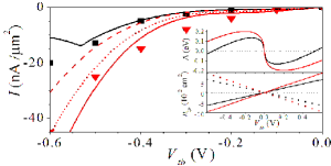
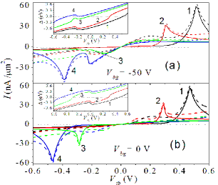
For the back-gated structure with -layer BN barriers (4 and 6) and 0.3 the dependencies of versus at fixed are shown in Fig. 3 at , when . 17 The electron (hole) concentrations are and is the sum of linear and square-root functions, see insets. The current-voltage characteristics are in reasonable agreement with the experimental data of Ref. 8 if we used the scale factor with the above-estimated and . The dependencies on are weak enough (25% for 4 and 10% for 6, not shown). If 0, when -0.55 V for 6-layer barrier, a negative resonant contribution due to dissipative tunneling gives 30% variations of the - characteristic. Such a peculiarity was not found in Ref. 8; probably, it is due to a lateral redistributions of charges or a large-scale inhomogeneities of the samples used. The - characteristics of back-gated structures at are plotted in Fig. 4 for 4, 6 and , 0. Once again, there is a reasonable agreement of with the available experimental data for 4 at . A visible asymmetry of takes place if but deviations from experimental data increase. The dependencies for are similar but is 2-times weaker and the resonant dissipative contribution is absent for 25 V because , see inset.
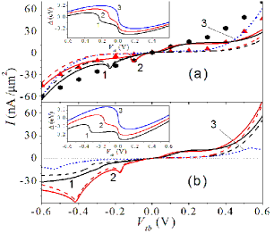
An enhancement of the resonant dissipative tunneling contributions takes place in the double-gated (four-terminal) structure, when depends on , , and . These dependencies are shown in Fig. 5 for the structure with 10-layer BN cover layer (3.4 nm; with a negligible tunneling, if 2 nm 18 ) at different top- and back-gate voltages ( corresponds to the three-terminal structure). Since the condition is realized now at higher energies, the resonant dissipative tunneling peaks are 10 times greater than the background current. This is the central result which should be important for the transistor applications. Note, that for 0 at 0 (the curve 3 in Fig. 5a) the resonant dissipative peak is suppressed. Beyond of this narrow region, the resonant condition should not be suppressed by lateral inhomogeneities and the peaks caused by the resonant dissipative tunneling should not be smeared.
Overall, the consideration presented here gives an adequate theoretical description of the tunneling transistor effect which is in reasonable agreement with the experimental data. 8 The analysis performed opens a way for the verification of scattering mechanisms and tunneling parameters in G/BN/G structures. In addition, the double-gated (four-terminal) structure was not considered before and this structure show a great (ten times) enhancement of tunneling current tunability.
IV Conclusion
We have adopted the theory of low-dimensional tunneling 4 ; 6 to the case of the tunneling charge transfer in independently contacted graphene structures with multi-layer BN barrier taking into account the two basic mechanisms of charge transfer: resonant dissipative tunneling and non-dissipative tunneling. Both the non-dissipative tunneling current and the non-resonant dissipative tunneling processes are responsible for the current-voltage characteristics of back-gated structures. 8 The resonant dissipative tunneling regime is achieved for the double-gated structures and these devices demonstrate a ten times enhancement of - characteristics which is important for transistor applications.
Further, we discuss the assumptions used. Because of a luck of data on stacking order in G/BN/G structures the tunneling energies and were estimated from the current-voltage characteristics of Ref. 8 and this result is in agreement with the tight-binding model. 14 More accurate estimates for and should be based on additional structural measurements. The simplified electrostatics description, given by Eq. (11), fails for the low-doped Gt- or Gb-layers, under weak interlayer fields applied. In these narrow regions, a more complicated description, which involves the quantum capacitance effect and the contact phenomena, should be applied. The rest of assumptions (the model of elastic scattering, 15 identical scattering in Gt,b-layers, weakness of long-range disorder, and the single-particle approach) are rather standard.
To conclude, we believe that the description of tunneling processes is an essential part of physics of graphene and the results obtained can be applied for characterization of scattering mechanisms and tunneling parameters in the tunnel-coupled graphene structures. More importantly, that these results open a way for improvement of tunneling transistor, a new type of graphene-based device. We believe that our study will stimulate a further investigation of these device applications.
*
Appendix A Tunneling Hamiltonian
Below we describe the tunnel-coupled states in G/BN/G structure using the 6-column wave function which is written through the spinors correspond to the Gt and Gb graphene layers. These layers are connected through the spinor described the single BN-layer. Within the tight-binding approach, 14 the eigenstate of energy is determined by the problem written through the Hamiltonian
| (15) |
where and are the Hamiltonians of Gt, Gb, and BN-layers, while and describe weak interlayer coupling of Gt and Gb sheets with BN layer. Under a transverse voltage applied, , where is the Hamiltonian of single graphene layer and is a splitting energy between the cross-points in Gt- and Gb-layers. For the low-energy (1 eV) states, if where 3.4 eV and -1.4 eV are the - and -band extrema energies in BN, we can eliminate the spinor from the system (A.1). As a result, the eigenstate problem is determined by the effective tunneling Hamiltonian
| (16) |
Here the matrix describes tunneling through BN insulator, while and correspond to the tunneling renormalization of - and -states:
| (17) | |||
Thus, we arrive to the Hamiltonian (1) with the renormalization contributions included to ; these corrections are negligible for the weak tunneling regime.
For the case of -layer BN insulator, we consider the -column wave function with -spinors described the BN layers. These states are coupled by the interlayer hopping matrices and which are placed to upper and lower sub-diagonals of Hamiltonian. 14 After eliminations of the spinors from the tight-binding eigenstate problem, we arrive to Eq. (A.3) where the non-diagonal matrix is replaced by
| (18) |
For the numerical estimates of and given by Eq. (8) we assume that the diagonal matrix is of the order of where is determined by . The hopping matrices , , and are estimated by the interlayer overlap integral and they are strongly dependent on a stacking order of G/BN/G structure.
References
- (1) E. L. Wolf, Principles of Electron Tunneling Spectroscopy, (Oxford University Press Inc., New York, 2012).
- (2) J. Smoliner, E. Gornik, and G. Weimann, Phys. Rev. B 39, 12 937 (1989); J. P. Eisenstein, Superlatt. and Microstruct. 12 107 (1992).
- (3) J. Wang, P. H. Beton, N. Mori, L. Eaves, H. Buhmann, L. Mansouri, P. C. Main , T. J. Foster, and M. Henini, Phys. Rev. Lett. 73 1146 (1994); N. Mori, P. H. Beton, J. Wang, and L. Eaves, Phys. Rev. B 51 1735 (1995).
- (4) R. F. Kazarinov and R. A. Suris, Sov. Physics - Semiconductors, 6, (1972).
- (5) J. P. Eisenstein, T. J. Gramila, L. N. Pfeiffer, and K. W. West, Phys. Rev. B 44, 6511 (1991); J. A. Simmons, S. K. Lyo, J. F. Klem, M. E. Sherwin, and J. R. Wendt, Phys. Rev. B 47, 15741 (1993).
- (6) L. Zheng and A. H. MacDonald, Phys. Rev. B 47, 10619 (1993); O. E. Raichev and F. T. Vasko, Journ. of Phys. Cond. Matter, 8, 1041 (1996).
- (7) L. A. Ponomarenko, A. K. Geim, A. A. Zhukov, R. Jalil, S. V. Morozov, K. S. Novoselov, I. V. Grigorieva, E. H. Hill, V.V. Cheianov, V. I. Falko, K. Watanabe, T. Taniguchi, and R. V. Gorbachev, Nature Physics 7, 958 (2011).
- (8) L. Britnell, R. V. Gorbachev, R. Jalil, B. D. Belle, F. Schedin, M. I. Katsnelson, L. Eaves, S. V. Morozov, N. M. R. Peres, J. Leist, A. K. Geim, K. S. Novoselov, and L. A. Ponomarenko, Science 335, 947 (2012).
- (9) K. S. Novoselov, A. K. Geim, S. V. Morozov, D. Jiang, Y. Zhang, S. V. Dubonos, I. V. Grigorieva, and A. A. Firsov, Science 306, 666 (2004).
- (10) S. B. Kumar, G. Seol, and J. Guo, Appl. Phys. Lett. 101, 033503 (2012).
- (11) For general consideration of the tunneling Hamiltonian approach see Ref. 1 and monograph by F. T. Vasko and A. Kuznetsov, Electronic States and Optical Transitions in Semiconductor Heterostructures, (Springer, New York, 1998).
- (12) F. T. Vasko and O. E. Raichev, Quantum Kinetic Theory and Applications (Springer, New York, 2005).
- (13) T. Ando, J. Phys. Soc. Jpn. 75, 074716 (2006); T. Stauber, N. M. R. Peres, and A. H. Castro Neto, Phys. Rev. B 78, 085418 (2008); F. T. Vasko and V. V. Mitin, Phys. Rev. B 84, 155445 (2011).
- (14) We use the model of disorder with random potentials described by the Gaussian correlator , with the averaged amplitude , and the correlation length , if the cut-off energy exceeds the energy scale under consideration. For the low-energy region, , the model gives relaxation rate, i. e. we deal with a short-range scattering and the coupling constant is given by .
- (15) J. Slawinska, I. Zasada, and Z. Klusek, Phys. Rev. B 81, 155433 (2010); R. M. Ribeiro and N. M. R. Peres, Phys. Rev. B 83, 235312 (2011).
- (16) F. T. Vasko and V. Ryzhii, Phys. Rev. B 76, 233404 (2007); N. M. R. Peres, Rev. Mod. Phys. 82, 2673 (2010).
- (17) C. R. Dean, A. F. Young, I. Meric, C. Lee, L. Wang, S. Sorgenfrei, K. Watanabe, T. Taniguchi, P. Kim, K. L. Shepard, J. Hone, Nature Nanotechn. 5, 722 (2010).
- (18) From Eq. (9) one obtains , , and . According to Eq. (11), and are even functions of voltages, so that remains the same under or .
- (19) F. Amet, J. R. Williams, A. G. F. Garcia, M. Yankowitz, K. Watanabe, T. Taniguchi, and D. Goldhaber-Gordon, Phys. Rev. B 85, 073405 (2012).