A two-atom electron pump
The fabrication of single atom transistors Sellier2006 ; Pierre2010a ; Tan2010 ; Fuechsle2012 paved the way for electronics based on single dopants Koenraad2011 ; Pla2012 . Recently the spectrum of a single dopant was measured electrically by coupling two such devices Roche2012a . The next step towards promising functionalities for future nanoelectronics Morton2011 consists in manipulating a single electron over two dopants. Here we demonstrate electron pumping through two phosphorus donors in series implanted in a silicon nanowire. While quantized pumping is achieved in the low frequency adiabatic regime, we observe remarkable features at higher frequency when the charge transfer is limited by the different tunneling rates. The transitions between quantum states are modeled involving a Landau-Zener transition, allowing to reproduce in detail the characteristic signatures observed in the non-adiabatic regime.
Adiabatic charge pumping at zero d.c. bias, in contrast to stationary electronic transport at finite bias, results in a net direct current when exactly one electron is transferred during a cycle of period (Refs. Kouwenhoven1991, ; Pothier1992, ; Thouless1983, ). Motivated by metrological applications Pekola2012 , there has been a growing interest in the non-adiabatic regime where this period is comparable to the characteristic time which particles spend in the system Moskalets2002 ; Kaestner2008 ; Pellegrini2011 . All experiments so far were in either one of these regimes but were not subsequently tuned to both. The ultra-scaled electron pump presented here, where the usual large dots are replaced by real nanometer-size atomic orbitals, offers this unique opportunity.
Single atom transistors are now realized in different ways, including both random Tabe2010 or deterministic Shinada2005 ; Fuechsle2012 placement of the dopant atoms. Electron pumping through many donors has been reported in a larger structure Lansbergen2012 . Here, despite the stochastic implantation process, transport through two dopants is obtained because 3 gates control an extremely small volume of silicon (602060 nm3) in which the number of P dopants is only a few tens for a concentration of cm-3, below the metal-insulator transition (see Fig. 1). The parts of the wire uncovered by the gates and adjacent spacers are doped with arsenic donors at high concentration ( cm-3) to define conducting source and drain electrodes, separated by 60 nm. This number prevents transport through a single donor, which requires a much shorter structure Pierre2010a , but favors transport through two donors in series. Indeed a distance of 30 nm between the two donors yields a mean tunnel coupling of the order of 1 GHz Miller1960 , a good compromise between weak coupling and measurable current. Moreover we obtain separate control over the energy levels of the two dopants by splitting the top gate into two, which face each other at a distance of only 15 nm. Finally a voltage is applied to the substrate Roche2012a in order to tune the coupling between the dopants and the leads and rule out rectification effects Brouwer2001 , measured for instance in Ref. Chorley2012a, . Starting from a nearly perfect yield in terms of transistor behaviour, the final yield for two-dopant features remains higher than 50% for the geometry and doping level chosen here.
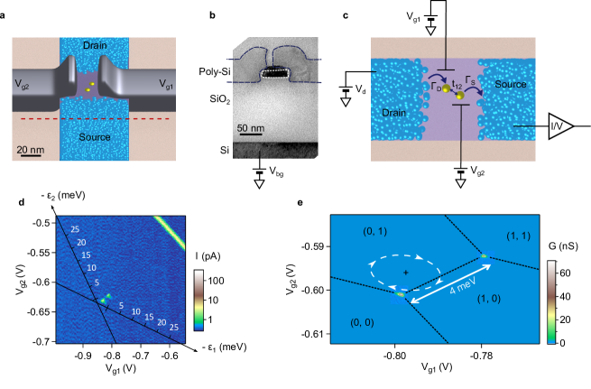
The sample is measured at 150 mK in a dilution refrigerator. The source-drain current is first measured with a fixed source-drain bias voltage to select two ideally placed dopants. The back gate voltage is changed until a set of triangles, characteristic of two levels in series Wiel2002 , is obtained when scanning the front gates (see Fig. 1d). This coupled donor system allows to perform atomic spectroscopy, in contrast with a single donor transistor based on the same technology where fluctuations of the local density of states dramatically affect the current at finite bias Vaart1995 . A large (10 meV) separation in energy between the ground and first excited states was measured in the same sample Roche2012a as investigated here. Besides this large valley-orbit splitting which makes it quite insensitive to a small bias, our 2-donor system is also well isolated in energy from any other states which could carry a current from source to drain (see Fig. 1d). The two triple points are separated by a Coulomb repulsion energy = 4.0 0.1 meV, which is markedly larger than any value reported so far Liu2008 .
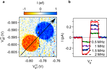
We now set to zero and modulate the top gates () with phase shifted sinewaves added to the d.c. voltages + sin(), in order to follow elliptical trajectories in the (, ) plane enclosing a triple point Pothier1992 (see Fig. 1e).
Adiabatic pumping occurs when the timescale of the driving is much larger than the timescale associated to tunneling to the leads for an electron in the 2-donor system, , and when there are no excitations in the internal dynamics due to the driving signal, requiring (see Eq. 1). Here is a tunneling rate, the difference in energy between the two levels, the speed at which they cross, the energy scale set by the temperature and the tunnel coupling between the two levels. Then the system follows the charge states given by the electrostatic stability diagram (Fig. 1e). Fig. 2 shows the normalized d.c. current measured in this regime. As expected we observe two circular regions of constant quantized current wherever a triple point is enclosed by the ellipse, and = 0 elsewhere. The sign of the current is reversed by changing the direction of the trajectory. The 2-atom system offers intriguing advantages compared to other quantized electron pumps, due to the large energies at play in this system. The large Coulomb repulsion energy between the dopants ensures wide and flat plateaus for the pumped current versus : a slope of 1.9 G is obtained over a range of 3.1 mV at 1 MHz (see Supplementary Information, Fig. S1). In contrast with metallic Coulomb islands co-tunneling events via intermediate virtual states are strongly suppressed due to the 10 meV single level-spacing for each of the dopants Roche2012a . Both these elastic cotunneling effects as well as remaining unwanted events due to inelastic tunneling are shown to be small.
At higher frequency the pumped current deviates from the fundamental relation = e. Figs. 3a,c show the current map for = 10 MHz 111The triple points are slightly shifted as compared to Figs. 1 and 2 because the sample was warmed up at room temperature in the meantime.. The two circular regions appearing when enclosing the triple points are still visible in Fig. 3c, but the current inside is not independent of the working point anymore. This is the first manifestation of the deviation from the adiabatic regime. The second remarkable feature is the occurence of extra current outside these circular regions. This effect becomes dramatic in Fig. 3a, where, due to the vanishingly small surface area of the pumping cycle for = 175∘, no signal is expected in the adiabatic case.
The complex features observed in the non-adiabatic regime can be fully understood by means of the model depicted in Fig. 3e and described in detail in the Supplementary Information. The transitions occuring within the two dopants are described through the dynamics of the closed two-level system. A dissipative part of the dynamics accounts for the tunnel coupling to the source and drain. The transition rates between donor states due to tunneling to the leads are obtained from Fermi’s golden rule Ingold1992 and are proportional to the tunneling rates to source and drain ( and ). Hopping of an electron between the two dopants, with tunnel amplitude , can occur when the two levels cross each other and the resulting time evolution of the two-level system is described according to the Landau-Zener problem Zener1932 . Consequently, the probability of staying on the same dopant after the crossing, i.e. the transition from ground to excited state, is given by the Landau-Zener transition probability . Then the probability for an electron to move from one dopant to the other when the levels are aligned depends on the speed and is given by,
| (1) |
The strict separation of the dynamics of the closed system and of the coupling to the reservoirs is possible because the time during which the levels cross, , is of the order of ns and thus much smaller than the time scale related to the dissipative dynamics, .
Using the electrostatic couplings obtained from the d.c. measurements we reproduce the various features observed in the experiment with a unique set of parameters ( = 670 MHz, = 18 MHz and = 610 MHz), as illustrated in Figs. 3b,d for = 175∘ and = 100∘. The whole set of phase differences is simulated with the same fidelity (see Supplementary Material, Animation 1). If nonadiabatic, the system does not necessarily relax to the ground state, either due to slow tunneling to the leads or due to its internal dynamics ( differs significantly from zero, if the condition is no longer fulfilled). Each case yields characteristic features we discuss in the following.
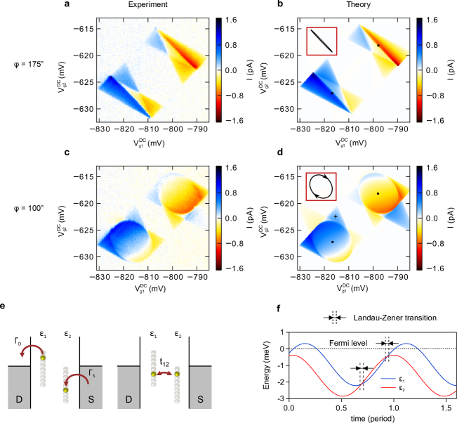
We focus on the working point indicated by the black cross in Fig. 3d. In this region no current is detected in the adiabatic regime. The time evolution of the energy levels is shown in Fig. 3f 222Although the phase shift of the two driving voltages have a phase difference = 100∘ the energy level of the two dopants are phase shifted only by 44∘ due to the cross-talk between the gates and dopants, see supplementary materials for more details.. Dopant 2 can accept electrons only from the drain and not from dopant 1 because it always lies below the Fermi level. After the electron moves to the dopant 1, its energy can be raised above the Fermi level, and it is eventually released into the drain lead. The key point here is that the transition probability between the two discrete dopant levels is different from one, otherwise the electron sitting on dopant 1 would go back to the initial dopant 2 after the second level crossing. This missed tunnel event due to the Landau-Zener transition occuring with probability in the non-adiabatic regime increases significantly the error rate Keller1996 . Indeed, for this working point, we get 0.25 from the simulation for both crossings. In contrast, at low enough frequencies the electron always stays on the lowest energy level according to the adiabatic theorem (). Also the rightmost red non-adiabatic feature can be understood in these terms.
The non adiabatic feature inside the circle is of different origin: here, it is the tunneling dynamics which matters. Even though is driven from above to below the Fermi energy before , the slow tunneling dynamics, , allows to charge dopant 1 first instead of 2. This effect is important in particular if the coupling between dopant 1 and the drain is much stronger than the coupling between dopant 2 and the source. Indeed, is fulfilled in the experiment, giving rise to the sign change within the circle. Note that this effect would survive even in the limit of , hence it does not rely on a non-adiabatic level crossing. The additional features can be understood analogously and are influenced by the individual coupling strengths and , with the exception of one feature that will be discussed in the following.
In order to reproduce the faint side triangle along the anti-diagonal, visible in Fig. 3d, we finally add a small effective inelastic relaxation rate = 14 MHz between levels to the model. However this rate has a very limited impact on the overall pumped current. For the working point indicated by the cross, the simulation shows that only 10 % of the total current comes from this inelastic term, the remaining 90 % being due to the elastic coupling . A much higher inelastic rate would suppress the current coming from the Landau-Zener transition.
Importantly, the ultimate atomic size of the system is crucial to get large level separation and strong Coulomb interaction. This enables us to use driving amplitudes corresponding to an energy level modulation of 2.5 meV, much higher than the electronic temperature (300 mK) in the contact, equivalent to 25 eV. As a consequence the pumped current signal has remarkably sharp borders between different pumping regions, allowing a detailed study of the mechanisms at play in each of these regions. Moreover, due to the large amplitudes, inter-level transitions occur far away (with respect to ) from the resonances with the leads, which justifies the zero temperature approach for our model. Finally, since the crucial parameter determining the non-adiabaticity is the speed of the crossing, the actual frequency to observe these effects depends on the size of the ellipse. With the large amplitudes we use the crossover is significantly lowered towards lower frequencies, making it easily accessible experimentally.
We have investigated electron pumping through two dopant atoms connected in series and addressed with three gates. We achieved quantized pumping in the adiabatic regime and, studying the crossover to the non-adiabatic regime, observed additional features in the pumping current. A model taking into account the tunnel couplings to the leads and between the two donors energy levels reproduces all the details of the measured pumped current. This ultimate size system behaves like a nearly perfect two-level system, and the full control of the well separated states in the dopants opens new opportunities for the study of pure spin pumping in a quantum system contacted to ferromagnetic leads Riwar2010 and for transporting quantum information Greentree2004 .
References
- (1) Sellier, H. et al. Transport spectroscopy of a single dopant in a gated silicon nanowire. Phys. Rev. Lett. 97, 206805 (2006).
- (2) Pierre, M. et al. Single-donor ionization energies in a nanoscale cmos channel. Nature Nanotech. 5, 133–137 (2010).
- (3) Tan, K. Y. et al. Transport spectroscopy of single phosphorus donors in a silicon nanoscale transistor. Nano Letters 10, 11–15 (2010).
- (4) Fuechsle, M. et al. A single-atom transistor. Nat Nano 7, 242–246 (2012).
- (5) Koenraad, P. M. & Flatte, M. E. Single dopants in semiconductors. Nat Mater 10, 91–100 (2011).
- (6) Pla, J. J. et al. A single-atom electron spin qubit in silicon. Nature 489, 541–545 (2012).
- (7) Roche, B. et al. Detection of a large valley-orbit splitting in silicon with two-donor spectroscopy. Phys. Rev. Lett. 108, 206812 (2012).
- (8) Morton, J. J. L., McCamey, D. R., Eriksson, M. A. & Lyon, S. A. Embracing the quantum limit in silicon computing. Nature 479, 345–353 (2011).
- (9) Kouwenhoven, L. P., Johnson, A. T., van der Vaart, N. C., Harmans, C. J. P. M. & Foxon, C. T. Quantized current in a quantum-dot turnstile using oscillating tunnel barriers. Phys. Rev. Lett. 67, 1626–1629 (1991).
- (10) Pothier, H., Lafarge, P., Urbina, C., Esteve, D. & Devoret, M. H. Single-electron pump based on charging effects. EPL (Europhysics Letters) 17, 249 (1992).
- (11) Thouless, D. J. Quantization of particle transport. Phys. Rev. B 27, 6083–6087 (1983).
- (12) Pekola, J. P. et al. Single-electron current sources: towards a refined definition of ampere. arXiv:1208.4030 (2012).
- (13) Moskalets, M. & Büttiker, M. Floquet scattering theory of quantum pumps. Phys. Rev. B 66, 205320 (2002).
- (14) Kaestner, B. et al. Single-parameter nonadiabatic quantized charge pumping. Phys. Rev. B 77, 153301 (2008).
- (15) Pellegrini, F. et al. Crossover from adiabatic to antiadiabatic quantum pumping with dissipation. Phys. Rev. Lett. 107, 060401 (2011).
- (16) Tabe, M. et al. Single-electron transport through single dopants in a dopant-rich environment. Phys. Rev. Lett. 105, 016803 (2010).
- (17) Shinada, T., Okamoto, S., Kobayashi, T. & Ohdomari, I. Enhancing semiconductor device performance using ordered dopant arrays. Nature 437, 1128–1131 (2005).
- (18) Lansbergen, G. P., Ono, Y. & Fujiwara, A. Donor-based single electron pumps with tunable donor binding energy. Nano Letters 12, 763–768 (2012).
- (19) Miller, A. & Abrahams, E. Impurity conduction at low concentrations. Phys. Rev. 120, 745–755 (1960).
- (20) Brouwer, P. W. Rectification of displacement currents in an adiabatic electron pump. Phys. Rev. B 63, 121303 (2001).
- (21) Chorley, S. J., Frake, J., Smith, C. G., Jones, G. A. C. & Buitelaar, M. R. Quantized charge pumping through a carbon nanotube double quantum dot. Appl. Phys. Lett. 100, 143104–3 (2012).
- (22) van der Wiel, W. G. et al. Electron transport through double quantum dots. Rev. Mod. Phys. 75, 1 (2002).
- (23) van der Vaart, N. C. et al. Resonant tunneling through two discrete energy states. Phys. Rev. Lett. 74, 4702–4705 (1995).
- (24) Liu, H. W. et al. Pauli-spin-blockade transport through a silicon double quantum dot. Phys. Rev. B 77, 073310– (2008).
- (25) Ingold, G.-L. & Nazarov, Y. V. Single Charge Tunneling, chap. Charge Tunneling Rates in Ultrasmall Junctions (Plenum Press, New York, 1992).
- (26) Zener, C. Non-adiabatic crossing of energy levels. Proceedings of the Royal Society of London. Series A 137, 696–702 (1932).
- (27) Keller, M. W., Martinis, J. M., Zimmerman, N. M. & Steinbach, A. H. Accuracy of electron counting using a 7-junction electron pump. Applied Physics Letters 69, 1804–1806 (1996).
- (28) Riwar, R.-P. & Splettstoesser, J. Charge and spin pumping through a double quantum dot. Phys. Rev. B 82, 205308 (2010).
- (29) Greentree, A. D., Cole, J. H., Hamilton, A. R. & Hollenberg, L. C. L. Coherent electronic transfer in quantum dot systems using adiabatic passage. Phys. Rev. B 70, 235317 (2004).
Acknowledgements.
AcknowledgementsWe thank V. N. Golovach for fruitful discussions as well as D. Lafond and H. Dansas from CEA-LETI for the transmission electron microscope image. The authors acknowledge financial support from the EC FP7 FET-proactive NanoICT under Project AFSiD No 214989, the French ANR under Projects SIMPSSON and POESI and from the German Ministry of Innovation NRW.