Present address: ] Kavli Institute of NanoScience, Delft University of Technology, 2600 GA, Delft, The Netherlands
Signatures of the Valley Kondo Effect in Si/SiGe Quantum Dots
Abstract
We report measurements consistent with the valley Kondo effect in Si/SiGe quantum dots, evidenced by peaks in the conductance versus source-drain voltage that show strong temperature dependence. The Kondo peaks show unusual behavior in a magnetic field that we interpret as arising from the valley degree of freedom. The interplay of valley and Zeeman splittings is suggested by the presence of side peaks, revealing a zero-field valley splitting between 0.28 to 0.34 meV. A zero-bias conductance peak for non-zero magnetic field, a phenomenon consistent with valley non-conservation in tunneling, is observed in two samples.
The valley degree of freedom of conduction band electrons is one of several intriguing properties distinguishing silicon from III-V materials. The six-fold valley degeneracy in bulk Si is reduced to two-fold in Si/SiGe heterostructures due to the confinement of electrons in a two-dimensional electron gas (2DEG). The resulting valley splitting in strained Si quantum dots (QD) and quantum point contacts is typically of order 0.2 meV.Boykin et al. (2004); Goswami et al. (2007) A particularly interesting manifestation of valley physics would be the valley Kondo effect. The spin 1/2 Kondo effect comprehensively studied in GaAs quantum dotsGoldhaber-Gordon et al. (1998); Cronenwett et al. (1998); Vidan et al. (2006); Sasaki et al. (2000); van der Wiel et al. (2002); Kogan et al. (2003); Granger et al. (2005) is usually observed when there is an odd number of electrons in the QD, in which the spin of an unpaired electron is screened by spins in the leads to form a singlet, resulting in a conductance resonance at zero dc bias. When a magnetic field is applied, the QD spin states are split by the Zeeman energy , being the Landé factor and the Bohr magneton. The spin-Kondo resonance then splits into two peaks at , where is the applied source-drain voltage.Goldhaber-Gordon et al. (1998); Meir et al. (1993) On the other hand, Kondo effects in Si/SiGe QDs have only rarely been reported,Klein et al. (2007) and there have been recent studies of dopants in a Si fin-type field effect transistor.Tettamanzi et al. (2012) This is perhaps not surprising, since for the valley Kondo effect to occur, the energy associated with the Kondo temperature must be larger than the valley splitting , i.e. where is the Boltzmann constant, a rather stringent condition. Nonetheless, how the valley degeneracy in Si affects the Kondo effect in Si/SiGe QDs has been investigated theoreticallyShiau et al. (2007); Shiau and Joynt (2007) and found to share some resemblance with carbon nanotubes.Jarillo-Herrero et al. (2005) The addition of the valley degree of freedom allows for a new set of phenomena to emerge, since both spin and valley indices can be screened. Measurement of the valley Kondo effect could therefore help probe the nature of valley physics in Si/SiGe QDs, a topic of great importance considering their potential application in quantum computation.Zwanenburg et al. (2013) In particular, the question of how the valley index of an electron changesGamble et al. (2013) as it tunnels on and off a QD can be illuminated.
Here we report measurement of unconventional Kondo effects in two different Si/SiGe QD samples, one in perpendicular magnetic field and both in in-plane magnetic field . In both samples we observe conductance enhancement in two consecutive Coulomb diamonds, forbidden in a purely spin 1/2 Kondo effect. The resonances disappear as the temperature is raised above a few Kelvin. For Sample I, in one diamond there are two peaks at zero magnetic field which coalesce and broaden into a single peak as is increased. In an adjacent diamond, a zero-bias resonance persists for finite . For a different dot configuration of Sample I measured in , we observe similar persistent zero-bias resonances in two consecutive diamonds. For Sample II, there is a single resonance in one diamond which again does not split in non-zero . In an adjacent diamond we observe additional side peaks that converge and part again as is increased. We argue that these counterintuitive phenomena may arise from an interplay between the valley and spin degrees of freedom.
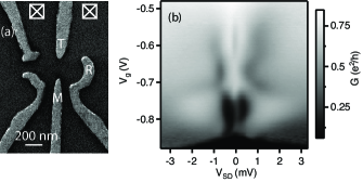
The Si/SiGe heterostructure is grown using chemical vapor deposition (CVD). A step-graded virtual substrate is grown on Si (001) that was miscut 2 degrees towards (010). A 1 m thick Si0.7Ge0.3 buffer layer is deposited next, followed by an 18 nm Si well where the two-dimensional electron gas (2DEG) is located. A 22 nm intrinsic layer, a 1 nm doped layer ( cm-3 phosphorous), a second intrinsic alloy layer of 50 to 75 nm, and last a 9 nm Si cap layer are grown subsequently. The devices are fabricated with low-leakage Pd gates.Yuan et al. (2011) Both QDs have the same design as shown in Fig. 1(a), formed by gates T, M, and R, and their differential conductance is measured with lock-in techniques. We perform measurements in two dilution refrigerators. In one refrigerator the sample is oriented perpendicular to the magnetic field while in the other it is aligned in-plane with the field. The base temperature corresponds to an electron temperature of mK in both refrigerators.
We begin by discussing measurements of Sample I in perpendicular magnetic field using an ac excitation of 3 V. Gates M and R in Fig. 1(a) are kept at V and V, respectively, while the voltage applied on gate T is varied. Interesting conductance enhancements appear in the Coulomb blockade region, as can be seen in the stability diagram of the QD differential conductance versus the dc bias voltage and the gate voltage shown in Fig. 1(b). There is a lower Coulomb diamond between and V and an upper one starting at V and extending towards the top of the figure. The relatively large size of this lower diamond ( between mV) suggests that the QD is in the few-electron regime, as observed in other Si/SiGe QDs of similar lithographic size and gate layout.Thalakulam et al. (2010); Shi et al. (2013) The lower diamond also shows inelastic co-tunneling features consisting of two roughly vertical regions of enhanced conductance for mV and mV that depend only weakly on . The co-tunneling is due to virtual transitions to an excited state with excitation energy of about 0.7 meV, indicating that it involves a change in orbital state rather than valley state, for which the excited state energies are typically smaller than meV. We make use of the co-tunneling feature’s implications for electron number in the QD De Franceschi et al. (2001) to estimate the charge states of the Coulomb diamond. Each energy level can be doubly occupied. For odd, elastic co-tunneling can always happen via an energetically favorable singly-occupied level instead of a higher level. Therefore, there will not be an abrupt enhancement of conductance at a certain bias voltage in the Coulomb blockade. For even on the other hand, for a co-tunneling event to take place an electron must virtually occupy a higher energy level, which can only happen when the bias voltage reaches the threshold determined by the energy level spacing. The results is a sudden step in the conductance at a non-zero bias. Thus the presence of inelastic co-tunneling in the lower diamond identifies it as corresponding to an even-electron-number state. The upper diamond must therefore correspond to an odd-electron-number state. We refer to the upper (lower) diamond as the odd (even)-number diamond. The Kondo effect in Si/SiGe QDs is forbidden for since the spin and valley states for a particular orbital state are filled.Shiau and Joynt (2007) Therefore, the even-number diamond corresponds to while the odd-number diamond corresponds to .
The Hamiltonian of a Kondo system with valley and spin degrees of freedom can be expressed as
| (1) |
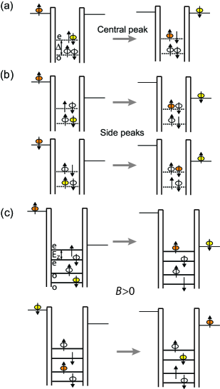
where creates (destroys) an electron with momentum , valley index , spin and energy in lead , and creates (destroys) an electron with valley index , spin and energy on the QD. The first two terms in (1) describe the energy of electrons in the leads and the QD, respectively. The third term is the Coulomb interaction, which is taken to forbid double occupancy, and the fourth term describes the transfer of electrons between states in the the leads with valley index and in the QD with valley index . When , the valley mixing is relatively strong. The ground state of is a combination of terms that can be visualized graphically as processes that involve the hopping of an electron from the left lead to the right lead. Each distinct process can give rise to a peak in the conductance if the amplitude of the process is large enough while unobserved processes indicate a small tunneling matrix element. The position of the peak can be read off from the energy change of the electron in the process, while the height of the peak depends on the tunneling amplitude that produces it. The processes resulting in the Kondo effect for a QD with are illustrated in Fig. 2, assuming that the valley splitting varies slowly with magnetic field compared to . Theory predicts three peaks for when the valley index is conserved: a peak at zero bias that involves a spin flip, commonly observed in GaAs QDs, and two valley side peaks that are due to changes in both spin and valley indices as the electrons tunnel through the QD.Shiau et al. (2007) A magnetic field should split each valley Kondo peak into three peaks, the distance between neighboring peaks being . In Fig. 2 two valley states with energy difference are labeled by and (the choice of as the lower state is arbitrary). Note, however, that since parity is not a good quantum number in the device, the states are not necessarily odd and even in the z-coordinate.
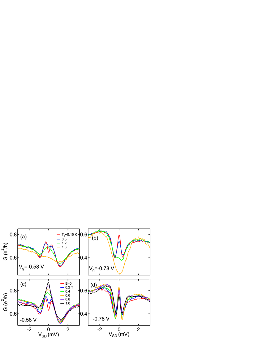
The temperature dependence of the resonances in the odd- and even-number diamonds is shown in Fig. 3(a) and (b), respectively, while their dependence on perpendicular magnetic field is shown in Fig. 3(c) and (d). As can be seen in Fig. 3(a) and (b), the resonances weaken as the temperature increases and vanish for K, verifying the presence of Kondo physics. There are several notable aspects of these resonances that contradict the spin-1/2 Kondo picture, such as a split resonance that coalesces into a single peak in the odd-number diamond and a single resonance in the even-number diamond that persists in as is increased. These seemingly counterintuitive phenomena are consistent with valley Kondo physics in the QD.
In the odd-number diamond, we find two conductance peaks, one on each side of zero dc bias, suggesting the presence of the valley effect, as illustrated in Fig. 2(b). Their position with respect to stays mostly the same within the diamond. We fix V, varying the temperature (Fig. 3(a)) and magnetic field (Fig. 3(c)). At mK, the two peaks are clear. As temperature is raised, the peaks broaden and their height decreases. At 1.2 K only a single broadened peak can be resolved; it eventually becomes difficult to discern at 1.8 K. Two characteristic temperatures are roughly estimated from the data in Fig. 3(a): K for the Kondo feature to appear and K to resolve the individual valley Kondo peaks.
Turning to the field dependence of these features in Fig. 3(c), as is increased the two peaks broaden and coalesce, becoming indistinguishable at =1 T. Associated tunneling processes are illustrated in Fig. 2(c). Note that the factor of Si is approximately 5 times larger than that of GaAs so that 1 T in these measurements is comparable to 5 T in GaAs QD experiments. The corresponding size of the Kondo peak splittingMeir et al. (1993) is approximately mV.
In Fig. 2(a) (), the conventional spin 1/2 Kondo effect that results in a central peak is illustrated; note that the processes involve tunneling to and from only an valley state. In contrast, Fig. 2(b) shows a process in which an electron occupying the valley state tunnels off the QD, and another electron from the lead tunnels on to the QD to occupy the state, resulting in the side peaks. The absence of a central peak in our experimental results suggests that the tunneling involving an odd valley is stronger than the pure even-valley tunneling and the Kondo temperature corresponding to the inter-valley process is higher than the spin-1/2 process. Therefore, at finite temperature, the side peaks are easier to observe while the center peak is obscured.
In this picture, the separation in of the two side peaks is twice the zero-field valley splitting in the QD, so meV. A magnetic field lifts the spin-degeneracy of each valley state. In Fig. 2(c) (), each valley state splits into two spin states with energy difference . A spin-down (up) electron in the state tunnels off the QD while a spin-up (down) electron tunnels on to the state, swapping both valley and spin indices. The other two processes remain degenerate, swapping only the valley index while preserving the spin index. As a result, the four processes generate three resonances in finite field. The resulting splitting broadens the two Kondo peaks and they coalesce into one peak, as shown in Fig. 3(c).
In the even-number diamond, there is a single resonance at zero bias. As shown in Fig. 3(b), the height of the resonance decreases monotonically with temperature, vanishing at 1.8 K. Surprisingly, as is increased this central resonance neither shifts nor splits, as shown in Fig. 3(d), which is significantly different from the Kondo effects previously reported in semiconductor QDs. To determine if a peak splits in non-zero magnetic field, we compare its full width at half maximum (FWHM) at zero field with the expected Kondo peak splitting . A peak is determined to be persisting near zero bias if double-peak structure is not observed at . For example Fig. 4 shows the magnetic field dependence of the Kondo resonance corresponding to V in Fig. 1(b). At 1 T the Kondo peak splitting corresponds to approximately mV for and the FWHM of the black curve in Fig. 4 is about 0.24 mV, so we determine that it does not split. In fact, a peak at zero dc bias that persists in a non-zero magnetic field is expected to be a signature of a pure valley Kondo state and is associated with processes in which the valley index is not conserved during tunneling.Shiau et al. (2007); Shiau and Joynt (2007) For the center peak involving only valley screening dominates while the side peaks are suppressed. This suggests that the Kondo temperature relating to the pure valley process is greater than that of the spin process, a result of strong valley mixing . Also, with the magnetic field perpendicular to the 2DEG, we expect some dependence of the tunneling matrix elements on , which might also be the reason why the peak height as well as the co-tunneling features show non-monotonic dependence on . The data taken in discussed in the following paragraph show monotonic field dependence.
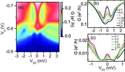
Sample I is also measured in a parallel magnetic field and once again we observe non-splitting Kondo peaks, this time for a different dot configuration. By measuring the QD in instead of the dependence on magnetic field of the tunnel matrix elements is reduced. Fig. 5(a) shows the stability plot of two consecutive charge states formed in this second dot configuration for . Gates M and R are kept at V and V respectively while gate T is swept by . A Kondo resonance at zero dc bias emerges in both charge states. When is increased, the center peaks in both diamonds persist without splitting even for T, as demonstrated in Fig. 5(b) for V and (c) for V. Since the factor in Si is about 5 times bigger than that in GaAs, 3 T here is comparable to 15 T for a GaAs based QD. The height of the peaks decreases monotonically with .
The appearance and persistence of the center peak with is a key prediction of the theory of the valley Kondo effect and arises physically from an interference of valley conserving and valley non-conserving processes. This suggests that valley index is not always conserved during tunneling, a subject of some debate,Jarillo-Herrero et al. (2005); Shiau et al. (2007); Tettamanzi et al. (2012); Friesen and Coppersmith (2010); Culcer et al. (2010); Friesen et al. (2006); Saraiva et al. (2011); Jiang et al. (2012, 2013) and in accord with recent effective mass calculations of the effects of atomic step disorder at the quantum well interface.Gamble et al. (2013) Secondly, given a non-zero , the QD electrons must occupy an excited state rather than the ground state viewed in terms of single-particle levels. This is allowed energetically since by forming the many-body state with the leads, the system gains energy. From the FWHM of the central peak in Fig. 3(d) we estimate this energy gain is on the order of meV, in good agreement with the temperature at which the resonance disappears. Assuming meV in the even-number diamond in Fig. 1(b), similar to that in the odd-number diamond, we have , recovering the condition for the valley Kondo effect to be observed.
Next we present measurements of Sample II in parallel magnetic field using an 8 V ac bias. Gates T and R are kept at V and V respectively while gate M is swept by . Again we find enhancement of conductance in two consecutive Coulomb diamonds. In one diamond the zero-bias conductance peak behaves in a similar fashion as Sample I, decreasing with increasing field without splitting. As shown in Fig. 6(a) taken at V, at there is a single Kondo resonance. It gradually decreases as increases and at T the Coulomb blockade is fully recovered.
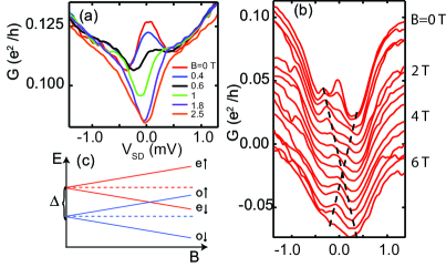
In an adjacent diamond with one fewer electron, some side peak features are resolved, suggesting comparable even and odd-valley coupling. In Fig. 6(b) taken at V we show a series of conductance curves offset by (0.0015 . The coexistence of the center resonance and the side resonance is consistent with a non-zero valley splitting. The center peak decreases with rising without obvious splitting. There are traces of two side peaks, indicated by the dashed lines, which move towards the center. After converging at about 3.5 T they move away from each other again. These features are mainly contributed by the Zeeman splitting of the valley side peaks similar to that illustrated in Fig. 2(b), revealing a zero-field valley splitting of about 0.34 meV. In Fig. 6(c) a schematic energy diagram of the valleys in the magnetic field is shown. The position of either side peak in Fig. 6(b) is determined by the relative distance between and in Fig. 6(c). The factors extracted from the two dashed lines (Fig. 6(b)) are about 1.8 and 1.5 respectively, smaller than but comparable to the standard value of . The asymmetry inside the Coulomb blockade suppresses the Kondo peak at positive bias, resulting in a very weak signal that is hard to read. Nonetheless, the data are consistent with interplay between the spin and valley degrees of freedom, a phenomenon recently observed in ESR experiments in silicon quantum dots.Hao et al.
In Fig. 7 we demonstrate at zero magnetic field the temperature dependence of the Kondo features shown in Fig. 6(b). Both the center peak and the side peak are reduced by rising temperature. At 0.6 K the peaks are significantly suppressed and the side peak becomes hard to discern. At 1.0 K both peaks are overcome by the Coulomb Blockade. The linewidth of the center peak, 0.18 mV, corresponds to a temperature of 2.1 K; for the side peak, the linewidth of 0.1 mV corresponds to 1.2 K. These results are in reasonable agreement with the measured temperature dependence of the features.
In conclusion, we have measured Kondo effects in two separate Si/SiGe QDs. Kondo peaks that diminish with rising temperature are present in one pair of consecutive Coulomb diamonds in one sample (Sample II), and in two separate pairs of consecutive diamonds in the other (Sample I), for a total of six separate dot configurations. From side peak positions at zero field due to valley screening, zero-field valley splitting is revealed to be meV in Sample I and meV in Sample II. A zero-bias conductance peak that persists for finite magnetic field, which is consistent with the valley Kondo effect due to valley non-conservation in tunneling, is repeatedly observed in both samples, in a total of five separate Coulomb diamonds. The experiment suggests that the valley degree of freedom in Si can enrich the Kondo effect in Si/SiGe QDs and requires better theoretical understanding.


Acknowledgements.
We would like to thank J. Stettenheim for assistance with the dilution refrigerator. This work is supported at Dartmouth and UW-Madison by the Army Research Office under Grant No. W911NF-12-1-0607 and at Dartmouth by the NSF under Grant No. DMR-1104821. Development and maintenance of the UW-Madison growth facilities used for fabricating samples is supported by DOE Grant No. DE-FG02-03ER46028.References
- Boykin et al. (2004) T. B. Boykin, G. Klimeck, M. A. Eriksson, M. Friesen, S. N. Coppersmith, P. von Allmen, F. Oyafuso, and S. Lee, Appl. Phys. Lett. 84, 115 (2004).
- Goswami et al. (2007) S. Goswami, K. A. Slinker, M. Friesen, L. M. McGuire, J. L. Truitt, C. Tahan, L. J. Klein, J. O. Chu, P. M. Mooney, D. W. van der Weide, R. Joynt, S. N. Coppersmith, and M. A. Eriksson, Nat. Phys. 3, 41 (2007).
- Goldhaber-Gordon et al. (1998) D. Goldhaber-Gordon, H. Shtrikman, D. Mahalu, D. Abusch-Magder, U. Meirav, and M. A. Kastner, Nature 391, 156 (1998).
- Cronenwett et al. (1998) S. M. Cronenwett, T. H. Oosterkamp, and L. P. Kouwenhoven, Science 281, 540 (1998).
- Vidan et al. (2006) A. Vidan, M. Stopa, R. M. Westervelt, M. Hanson, and A. C. Gossard, Phys. Rev. Lett. 96, 156802 (2006).
- Sasaki et al. (2000) S. Sasaki, S. D. Franceschi, J. M. Elzerman, W. G. van der Wiel, S. T. M. Eto, and L. P. Kouwenhoven, Nature 405, 764 (2000).
- van der Wiel et al. (2002) W. G. van der Wiel, S. De Franceschi, J. M. Elzerman, S. Tarucha, L. P. Kouwenhoven, J. Motohisa, F. Nakajima, and T. Fukui, Phys. Rev. Lett. 88, 126803 (2002).
- Kogan et al. (2003) A. Kogan, G. Granger, M. A. Kastner, D. Goldhaber-Gordon, and H. Shtrikman, Phys. Rev. B 67, 113309 (2003).
- Granger et al. (2005) G. Granger, M. A. Kastner, I. Radu, M. P. Hanson, and A. C. Gossard, Phys. Rev. B 72, 165309 (2005).
- Meir et al. (1993) Y. Meir, N. S. Wingreen, and P. A. Lee, Phys. Rev. Lett. 70, 2601 (1993).
- Klein et al. (2007) L. J. Klein, D. E. Savage, and M. A. Eriksson, Appl. Phys. Lett 90, 033103 (2007).
- Tettamanzi et al. (2012) G. C. Tettamanzi, J. Verduijn, G. P. Lansbergen, M. Blaauboer, M. J. Calderón, R. Aguado, and S. Rogge, Phys. Rev. Lett. 108, 046803 (2012).
- Shiau et al. (2007) S.-Y. Shiau, S. Chutia, and R. Joynt, Phys. Rev. B 75, 195345 (2007).
- Shiau and Joynt (2007) S.-Y. Shiau and R. Joynt, Phys. Rev. B 76, 205314 (2007).
- Jarillo-Herrero et al. (2005) P. Jarillo-Herrero, J. Kong, H. S. J. van der Zant, C. Dekker, L. P. Kouwenhoven, and S. D. Franceschi, Nature 434, 484 (2005).
- Zwanenburg et al. (2013) F. A. Zwanenburg, A. S. Dzurak, A. Morello, M. Y. Simmons, L. C. L. Hollenberg, G. Klimeck, S. Rogge, S. N. Coppersmith, and M. A. Eriksson, Rev. Mod. Phys. 85, 961 (2013).
- Gamble et al. (2013) J. K. Gamble, M. A. Eriksson, S. N. Coppersmith, and M. Friesen, Phys. Rev. B 88, 035310 (2013).
- Yuan et al. (2011) M. Yuan, F. Pan, Z. Yang, T. J. Gilheart, F. Chen, D. E. Savage, M. G. Lagally, M. A. Eriksson, and A. J. Rimberg, Appl Phys Lett 98, 142104 (2011).
- Thalakulam et al. (2010) M. Thalakulam, C. B. Simmons, B. M. Rosemeyer, D. E. Savage, M. G. Lagally, M. Friesen, S. N. Coppersmith, and M. A. Eriksson, Appl. Phys. Lett. 96, 183104 (2010).
- Shi et al. (2013) Z. Shi, C. B. Simmons, D. R. Ward, J. R. Prance, R. T. Mohr, T. S. Koh, J. K. Gamble, X. Wu, D. E. Savage, M. G. Lagally, M. Friesen, S. N. Coppersmith, and M. A. Eriksson, Phys. Rev. B 88, 075416 (2013).
- De Franceschi et al. (2001) S. De Franceschi, S. Sasaki, J. M. Elzerman, W. G. van der Wiel, S. Tarucha, and L. P. Kouwenhoven, Phys. Rev. Lett. 86, 878 (2001).
- Friesen and Coppersmith (2010) M. Friesen and S. N. Coppersmith, Phys. Rev. B 81, 115324 (2010).
- Culcer et al. (2010) D. Culcer, X. Hu, and S. Das Sarma, Phys. Rev. B 82, 205315 (2010).
- Friesen et al. (2006) M. Friesen, M. A. Eriksson, and S. N. Coppersmith, Appl. Phys. Lett. 89, 202106 (2006).
- Saraiva et al. (2011) A. L. Saraiva, M. J. Calderon, R. B. Capaz, X. Hu, S. Das Sarma, and B. Koiller, Phys. Rev. B 84, 155320 (2011).
- Jiang et al. (2012) Z. Jiang, N. Kharche, T. Boykin, and G. Klimeck, Appl. Phys. Lett. 100, 103502 (2012).
- Jiang et al. (2013) L. Jiang, C. H. Yang, Z. Pan, A. Rossi, A. S. Dzurak, and D. Culcer, Phys. Rev. B 88, 085311 (2013).
- (28) X. Hao, R. Ruskov, M. Xiao, C. Tahan, and H.-W. Jiang, “Electron spin resonance and spin-valley physics in a silicon double quantum dot,” arXiv:1311.5937.