2012 \MonthDecember \Vol55 \No12 \BeginPage1 \EndPage14 \AuthorMarkFeng W X, et al. \AuthorMarkCiteFeng W X, et al.. \DOI10.1007/s11433-012-4929-9
Three-dimensional topological insulators: A review on host materials
Abstract
In recent years, three-dimensional topological insulators (3DTI) as a novel state of quantum matter have become a hot topic in the fields of condensed matter physics and materials sciences. To fulfill many spectacularly novel quantum phenomena predicted in 3DTI, real host materials are of crucial importance. In this review paper, we first introduce general methods of searching for new 3DTI based on the density-functional theory. Then, we review the recent progress on materials realization of 3DTI including simple elements, binary compounds, ternary compounds, and quaternary compounds. In these potential host materials, some of them have already been confirmed by experiments while the others are not yet. The 3DTI discussed here does not contain the materials with strong electron-electron correlation. Lastly, we give a brief summary and some outlooks in further studies.
Received August 30, 2012; accepted October 22, 2012
Three dimension, topological insulator, host material
71.15.-m, 71.20.-b, 71.70.-d, 73.20.-r\CitFeng W X. Yao Y G. Three-dimensional topological insulators: A review on host materials. Sci China-Phys Mech Astron, 2012, doi: 10.1007/s11433-012-4929-9
1 Introduction
In the past few decades, topological quantum states characterized by specially topological orders [1,2] have become one of the most critical physical phenomena in condensed matter physics. In general concept, topological insulator contains two classes of topological quantum states depending on whether the system has time-reversal symmetry (TRS) or not. In the case of two-dimension, the first is the quantum Hall (QH) state [3], in which the TRS is explicit broken due to external magnetic field or internal magnetization. This topologically nontrivial state can be classified by the first Chern number proposed by Thouless et al. [2], directly connected to the quantized Hall conductivity. The second is the quantum spin Hall (QSH) state [4–6], which is protected by TRS and essentially resulted from spin-orbit coupling (SOC). Similar to the role of the Chern number, Z2 topological invariant in TRS protected systems was introduced by Kane and Mele [7], that is, Z2=1 (0) represents topologically nontrivial (trivial) state. The topological insulator with the common feature,
\qihao*Corresponding author (YAO Yugui, email: ygyao@bit.edu.cn)
having gaped insulating states in the bulk but gapless surface states on the edge, fundamentally distinguishes itself from the ordinary insulating state originally defined by Kohn [8].
The QSH state, i.e., two-dimensional topological insulator, has attracted research focus because of its promising applications in spintronic devices. The existence of QSH state in graphene was first proposed by Kane and Mele [5,6], however, subsequent works [9–11] showed that the band-gap induced by the SOC is too small ( 10-6 eV) and QSH state in graphene can not be observed in current experimental conditions. A more realistic material is the HgTe/CdTe quantum well, theoretically predicted by Bernevig et al. [12] and then experimentally confirmed by König et al. [13]. Soon after the QSH state was discovered, topological quantum states under TRS were also extended in three-dimension [14-16], i.e., the three-dimensional topological insulators (3DTI). In 3D, there are four Z2 topological invariants, , used to classify the topology of an insulator [17]. A nonzero indicates that the system is a strong topological insulator (STI). When =0, the systems are further classified according to , , and . The systems with =0 (not all of them) are called weak topological insulators (WTI), while 0;(000) is a normal insulator (NI). A STI can not be directly connected to a WTI or a NI by any adiabatically continuous transformation of band structure. In the WTI or NI, the surface states have an even number of Dirac points and can be violated by structural disorders or ferromagnetic impurities. Conversely, in the STI, the surface states have an odd number of Dirac points and are topologically protected.
The 3DTI is fascinating mainly because of its exotic surface states [18–21], which are very robust and against from the extrinsic perturbations, such as structural disorders and nonmagnetic impurities. Combining the topological surface state with superconducting state or ferromagnetic state, the 3DTI has shown great application potentials in quantum computing and spintronics fields [22–23]. So far many 3DTI host materials have been theoretically predicted and/or experimentally confirmed [see Table LABEL:tab1]. However, most of current 3DTI host materials have various disadvantages as observed in experimental observations, for example the large concentration of bulk carrier, which hinders further investigation along the direction of practical applications. Therefore, searching for new better host materials with simpler electronic structures and simpler synthetic conditions is a key step in this field.
In this review paper, we focus on the 3DTI host materials. We introduce general methods of searching for new 3DTI based on the density-functional theory. We also discuss many theoretically proposed 3DTI materials including simple elements, binary compounds, pseudo-binary compounds, ternary compounds, and quaternary compounds. In these potential host materials, some of them have already been confirmed by experiment while the others are not yet. The 3DTI discussed here does not contain the materials with strong electron-electron correlation.
2 How to search for 3D-topological insulators
As a first step towards various applications of 3DTI, material realization is of crucial importance. During the search of 3DTI in real materials, first-principles calculations guided by the topological band theory [18,19] have played a pivotal role. We briefly introduce four widely used methods to search 3DTI. In practice, two or more among these methods are usually combined together to determine the band topology of a crystal.
2.1 Surface state electronic structure
As a fundamental feature in 3DTI, there is gapless surface state inside the bulk band-gap [18–21]. The gapless surface state has the form of linear Dirac cone, which holds massless relativistic particles described by the Dirac equation [24,25]. Furthermore, the spin and momentum of surface Dirac electrons are locked together in the sense that the electrons with opposite spin must propagate in opposite direction along the boundary due to TRS. Hence, one can determine whether an insulator is a 3DTI or not by calculating the surface state electronic structure. An odd number of surface states crossing the Fermi level indicates a 3DTI, otherwise it is a normal insulator. At the experimental aspect, the surface state electronic structure can be directly measured by the angle-resolved photoemission spectroscopy (ARPES). The comparison between theoretical calculations and experimental ARPES measurements becomes possible.
Although the bulk-boundary correspondence as a basic routine can be used to find the topologically nontrivial materials, it is not effective in first-principles calculations. Physically speaking, the surface band dispersion is sensitive to the details of the surface, such as the terminations and orientations [26–28]. Furthermore, some topologically trivial states, for example the dangling bonds on the surface of group-IV or III-V semiconductors, may manifest themselves in the surface band structure. The surface reconstruction or hydrogen passivation can partly destroy these dangling bonds, but the coexistence of topologically trivial and nontrivial surface states certainly complicates the identification of the topological order. From the computational point of view, first-principles calculation of surface state electronic structure is an inefficient method because it generally requires a large amount of computational resources.
2.2 Adiabatic continuity band transformation
The argument of adiabatic continuity was once used to identify the quantum spin Hall phase in HgTe/CdTe quantum well [12] and silicene [29], but can also be introduced into the 3DTI. The basic idea is that the Hamiltonian of a system can be adiabatically connected to that of another system. For the former and latter systems, the topological invariants can only change when the bulk band-gap closed. Therefore, if the band structure of a material can be smoothly transformed to that of another one without closing the band-gap, then they must share the same topological classification. In contrast, if the band-gap closes during the band transformation, the topological phase transition may occur.
In practice, the adiabatic continuity transformation of band structure can be artificially controlled, for example, by altering the composition in solid alloy Bi1-xSbx [17,30,31] or Pb1-xSnxTe [17]. By starting from zero, these systems undergo the topological phase transition from trivial state to nontrivial state. If we continue increasing for Pb1-xSnxTe, a further transition from nontrivial state to trivial state will happen. Tuning other parameters, such as atomic number and strength of SOC, are also widely used in literatures. The obvious advantage of this method is its apparent ease. One can predict new 3DTI candidates based on some well-known topologically nontrivial or trivial materials. While many intermediate phases are required along the transformational path connecting the initial state and the final one, which makes this method computationally demanding.
2.3 Band inversion picture
Sometimes, topologically nontrivial materials can be well recognized at the first glance by the so-called band inversion picture [12]. In most of the common semiconductors, the valence band-edges are formed by the -orbits of electrons, whereas the conduction band-edges are formed by the -orbits of electrons. This situation belongs to normal band order, i.e., topologically trivial phase. In other cases, the relativistic effect from heavy elements can be so large that the -orbits is pushed below the -orbits, that is, the inverted band order appears. A typical example is HgTe in which the effective positive charge of Hg core is increased due to the partly delocalization of its -orbits. This causes the -orbits to be more attracted by the Hg core, and consequently, the -orbits are pushed below the -orbits. i.e., the inverted band structure forms [32].
The band inversion is a strong indication that a material falls into topologically nontrivial phase. The first application is the prediction of quantum spin Hall effect in HgTe/CdTe quantum well proposed by Bernevig et al. [12]. The quantum well structure is that the HgTe with inverted band order is sandwiched by the CdTe with normal band order. The topological property of entire quantum well is determined by the thickness of HgTe layer. The critical thickness is predicted to be about 6.5 nm [12]. For a thin well when , the CdTe has the dominant effect and the entire quantum well is topologically trivial with normal band order, while for a thick well when , the HgTe has a critical role role and the entire quantum well is topologically nontrivial with inverted band order.
Similar to HgTe and CdTe, the band topology of other cubic semiconductors with zinc-blende-like structure can also be determined by the band inversion picture. To do this, one need to define a useful physical quantity, namely, the band inversion strength (BIS). Specially at point, the BIS is defined as the energy differences between state (formed by -orbits) and state (formed by -orbits) [33,34] i.e.,
| (1) |
In general, negative typically indicates that the materials are in topologically nontrivial phase, while those with positive are in topologically trivial phase.
Moreover, the conventional -orbits semiconductors, the band inversion has also been found in -orbits and -orbits semiconductors. In Bi2Se3 family, both the valence and conduction band-edges are formed by -orbits but with opposite parities. It was predicted that Bi2Se3 family is 3DTI due to the inverted band order between and orbits [35]. Here, the () means the parity of the corresponding Bloch wavefuntions. The band inversion can be interpreted that at point these two -orbits with opposite parities are exchanged when SOC turns on. Other examples are actinide compounds Am (=N, P, As, Sb, and Bi) and Pu (=Se and Te), which were recently discovered by Zhang et al. [36] as a new class of 3DTI driven by strong electron-electron interactions. In these compounds, the state of 6-orbit locates below the state of 5-orbit at point, and as a result, the inverted band order occurs.
Although the band inversion at some high-symmetry points is a convenient way to find topologically nontrivial materials, for example HgTe/CdTe quantum well, Bi2Se3 family, and actinide compounds, it should be used with more care because the band topology is a global property within the entire Brillouin zone and is not only limited to some high-symmetry points.
2.4 Z2 topological invariants
The most general and direct method of searching for 3DTI is to calculate the topological invariants from the bulk band structure [14–16]. There exist two situations depending on whether the system has spatial inversion symmetry or not. If a system has inversion symmetry, the calculation of topological invariants can be well simplified based on the parity criterion developed by Fu and Kane [17]. Conversely, if a system does not have inversion symmetry, Fukui and Hatsugai [37] have developed an effective algorithm, which requires Bloch functions (BFs) on a dense two-dimensional grid to compute the Z2 topological invariants. The implementation of these two methods within full-potential linearized augmented plane-wave (FP-LAPW) formalism has been demonstrated [38]. In the following, we briefly introduce these two methods.
In the systems with inversion symmetry, the parity analysis only requires the knowledge of BFs on the time-reversal invariant momenta (TRIM) in the Brillouin zone (BZ) [17]. In 3D system, there are eight TRIMs, , where are primitive reciprocal-lattice vectors with . The invariants are determined by the quantities
| (2) |
Here, is the eigenvalue of parity operator at the 2m-th occupied band and TRIMs . The is equal to 1 (-1), corresponding to even (odd) parity of the BFs. The sum is over all of the occupied bands with only even band index due to the Kramers degeneracy at TRIMs. In 3D system, there are four independent invariants , given by [17]
| (3) |
| (4) |
where is independent of the choice of primitive reciprocal-lattice vectors while , , and are not. The combination of these four independent invariants clearly distinguish three classes of states: STI, WTI, and NI [17].
In the systems without inversion symmetry, an effective algorithm on a dense two-dimensional grid to compute the Z2 invariants has been proposed by Fukui and Hatsugai within a tight-binding framework [37]. It was shown that under the time-reversal constraint the invariants can be written in terms of the Berry gauge potential and Berry curvature associated with the BFs [39],
| (5) |
where and are the Berry connection and Berry curvature, respectively,
| (6) |
and
| (7) |
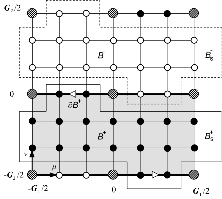
The and indicate half of 2D-torus and its boundary, respectively (see Fig. 1). By using the periodic gauge [40,41]
| (8) |
and two time-reversal constraints [37,39]
| (9) |
and
| (10) |
one can obtain the periodic part of BFs at every -point of the 2D-torus. Then, the Berry connection [Eq. (6)] and Berry curvature [Eq. (7)] can be calculated by the finite element expressions [37]. After that, the Z2 invariants can be obtained by inserting Eqs. (6) and (7) into Eq. (5). In 3D system, there are six 2D-tori , , , , , and , supporting six invariants , , , , , and . However, out of these six possible Z2 invariant only four of them are independent due to the constraint + = + = + (mod 2). The invariants are denoted in another way with , , and , i.e., [14–16]. By using topological invariants , one can determine the band topology for a given material.
Comparing with the surface state electronic structure (Sec. 2.1), adiabatic continuity band transformation (Sec. 2.2), and band inversion picture (Sec. 2.3), the calculation of the Z2 topological invariants is a direct evidence for determining topologically nontrivial state. Furthermore, from the viewpoint of first-principles calculation, it is the most computationally efficient. Our implementation of the calculation of Z2 topological invariants within FP-LAPW formalism has been recently applied to predict ternary half-Heusler [33,34] and chalcopyrite [42] 3DTI and quantum spin Hall effect in silicene thinfilm [29]. Since the critical factor is to calculate the eigenvalues of the parity operator and time-reversal operator in the systems with and without inversion symmetry respectively, it can be implemented in any other first-principles methods, such as the pseudopotential planewave and the linear muffin-tin orbital. There appears another approach to compute the invariants by employing the charge center of Wannier functions [43,44].
3 3DTI host materials
We review the 3DTI host materials in the sequence of simple elements, binary compounds, pseudo-binary compounds, ternary compounds, and quaternary compounds. In each part, only one or several typical materials are discussed. Table LABEL:tab1 includes a list of all 3DTI host materials. In these potential host materials, some of them have been confirmed by experiments while the others are not yet. The readers can find the interesting materials in Table LABEL:tab1 and refer to the literatures therein. It also should be noted that the 3DTI discussed here does not contain the materials with strong electron-electron correlation.
3.1 3DTI in simple elements
3.1.1 -Sn
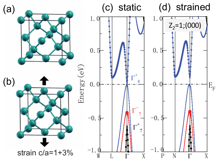
The group-IV element -Sn (grey tin) crystallizes in the diamond structure with space group Fdm (No. 227), as shown in Fig. 2(a). The full-relativistic band structure in Fig. 2(c) clearly shows that at the static lattice constant -Sn is a zero band-gap semiconductor with the feature of band inversion. The valence band maximum (VBM) and the conduction band minimum (CBM) are degenerated at point and the Fermi level crosses the fourfold-degenerated state (from -orbits). The -orbits-like state is situated below the state, forming the inverted band structure [48,49]. Hence, the band structure of -Sn is qualitatively different from those of the other group IV elements C, Si, and Ge [49].
Fu et al. [17] proposed that a uniaxial strain can tune -Sn into a 3DTI. The basic idea is that after applying a uniaxial strain the fourfold-degenerated state is lifted and a band-gap opens around point. Consequently, the topologically nontrivial state forms because the band inversion does not change. Fig. 2(d) shows the band structure of -Sn under a uniaxial strain c/a=1+3% but with constant volume. One can see that the band-gap opens while the band inversion preserves. To further confirm the argument of band inversion, the Z2 topological invariant is calculated. The result 1;(000) indicates that the strained -Sn is indeed a STI. Although the theoretical picture is very clear, there is not any experimental work on -Sn currently.
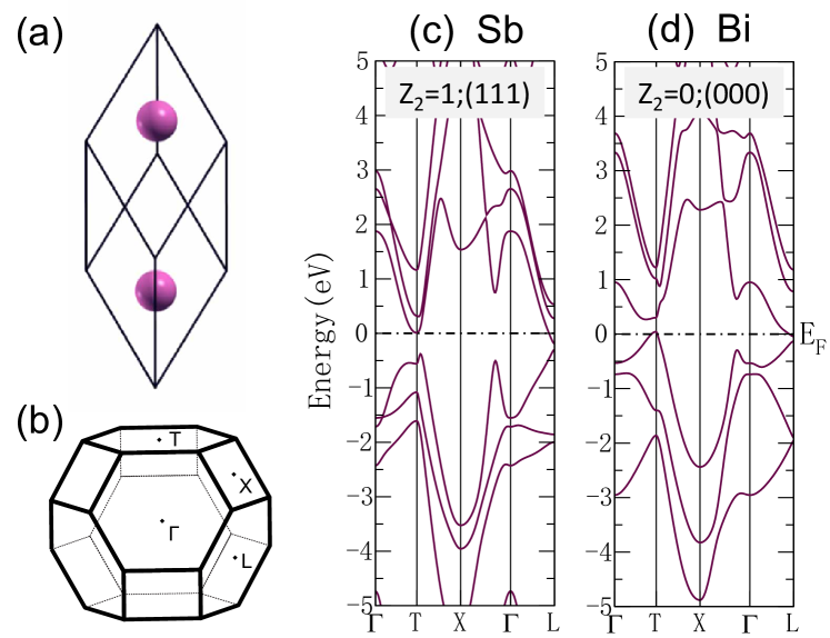
3.1.2 Sb
The Sb (antimony) crystallizes in rhombohedral structure with space group Rm (No. 166), as shown in Fig. 3(a). The full-relativistic band structure in Fig. 3(c) shows Sb is a semimetals with small pockets of electron in the vicinity of the L point. There are also small pockets of hole around the low-symmetry H point (not shown). Although it is not an insulator, Z2 topological invariant can still be defined because the local band-gaps (negative indirect band-gap) exist at every -point throughout the entire BZ [17]. The result 1;(111) indicates that the Sb is a STI. As another group-V element, Bi (bismuth) has similar crystal and band structure comparing to Sb, as shown in Fig. 3(a) and 3(d) respectively, but Bi is a NI with Z2 topological invariant 0;(000). The different topological classes between Sb and Bi were well interpreted by their different parities at L points [17].
Hsieh et al. [51,52] have measured the bulk and surface electronic structure of Sb. Because bulk Sb is a semimetal, it is difficult to separate its surface state from the projection of bulk state around the Fermi level. While by using advanced spin-resolved ARPES technique, Hsieh et al. [51] successfully isolated the surface states of Sb(111) from its bulk states over the entire BZ. They also directly found the gapless and spin-splitting surface state, which characterizes the topologically nontrivial feature in Sb [51].
3.2 3DTI in binary compounds
3.2.1 Bi1-xSbx alloy
Both Sb and Bi are group-V semimetals with the rhombohedral crystal structures and similar lattice constants, therefore, they can easily form solid alloy Bi1-xSbx [53]. By altering the concentration of Sb substitution, Bi1-xSbx undergoes a phase transition between semimetal and semiconductor. In the range of 0.07 0.22, Bi1-xSbx becomes semiconductor with the largest global band-gap of 0.03 eV at =0.18. Based on a tight-binding model [54], Fu et al. [17,30] predicted that Bi1-xSbx is the first realistic 3DTI material. Subsequently, this prediction was confirmed by first-principles calculation [31] and experimental observations [55–57].
Although both theories and experiments got a consistent conclusion that the topologically nontrivial phase exists in Bi1-xSbx alloy, the discrepancies about surface electronic structure still remain. The main concern is the surface band configuration, including the numbers of surface bands and the crossing times between the surface bands and the Fermi level along the - line in surface BZ. All the experimental works [55–57] reported three surface bands (, , and ) lying inside band-gap of bulk projection, but with different crossing times with the Fermi level, five times in Refs. [55,56] and three times in Ref. [57]. Conversely, both tight-binding [30] and first-principles [31] calculations can not reproduce the presence of the third surface band . Teo et al. [30] and Zhang et al. [31] give three and five times of band crossing, respectively. Therefore, more experimental measurements and theoretical calculations are needed for revealing the microscopic physics in Bi1-xSbx.
3.2.2 Bi2Se3 family
Since the surface electronic structure of Bi1-xSbx is rather complicated and its bulk band-gap is too small, searching for new 3DTI host materials with simple surface electronic structure and large band-gap becomes extremely important. Fortunately, Bi2Se3 family compounds with larger band-gap and simper surface spectrum have been found as a second generation of 3DTI materials [35,58–60], which support further study on various topologically protected phenomena at room temperature.
Tetradymite semiconductors Bi2Se3, Bi2Te3, and Sb2Te3, have a rhombohedral crystal structure with space group Rm (No. 166). Although Sb2Se3 essentially has an orthorhombic crystal structure, a virtual rhombohedral crystal structure is used at here for comparing its topological property with tetradymite semiconductors. Zhang et al. [35] theoretically proposed that Bi2Se3, Bi2Te3, and Sb2Te3 are 3DTI while Sb2Se3 is not. More importantly, the band-gap of Bi2Se3 is as large as 0.3 eV, which is larger than the energy scale of room temperature. Almost at the same time, these family compounds were experimentally confirmed with the observation of single Dirac cone on the surface for Bi2Se3 [58], Bi2Te3 [59,60], and Sb2Te3 [60]. Because of the large band-gap and simple surface electronic structure, Bi2Se3 family compounds have been extensively studied ranging from bulk to thinfilm [61–71].
3.2.3 HgTe and strained InSb
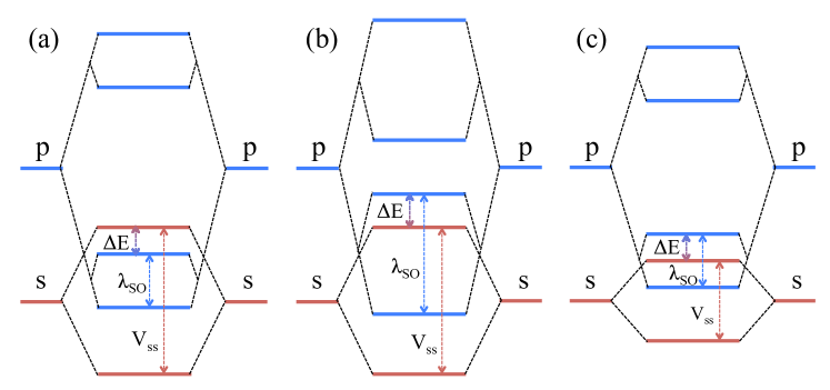
HgTe is a zinc-blende compound with space group F3m (No. 216). It is a zero band-gap semiconductor due to large relativistic effect. The twofold-degenerated state is located below the fourfold-degenerated state, forming the inverted band order [see Fig. 4(b)]. Fu et al. [17] theoretically predicted that HgTe is a 3DTI under a uniaxial strain. The basic routine is similar to that of -Sn, that is, the uniaxial strain is used to break the cubic symmetry and open a band-gap at point without changing the band inversion. Recently, Brüne et al. [72] successfully observed the Dirac-like topological surface state on strained HgTe by ARPES measurement.
InSb is also a zinc-blende semiconductor, but in contrast to HgTe, it has a small band-gap of 0.235 eV [74]. The state is located above the state, forming the normal band order [see Fig. 4(a)]. Feng et al. [75] proposed that InSb can be turned into a 3DTI by a 2% 3% biaxial lattice expansion. The generic guiding principle is that lattice expansion decreases the coupling potentials of -orbits or -orbits, which leads to the band inversion [see Fig. 4(c)]. Here, we use different modes of strain in HgTe and InSb. In the former one, the uniaxial strain is just used to break the cubic symmetry. While in the latter one, the nonhydrostatic (2% 3% biaxial) lattice expansion is twofold because it not only changes normal band order to inverted band order but also breaks the cubic symmetry.
3.3 3DTI in pseudo-binary compounds
Although Bi2Se3 family as the second generation of 3DTI has attracted research focus because of its simple surface electronic structure, it hard to be applied in various real devices. The prominent difficulty is high bulk carrier concentration, which remarkably masks the contribution of surface carriers in the surface transport measurement [55,62,80–82]. The high bulk carriers concentration mainly originates from the native crystal defects [58–60]. Some experimental techniques including compensate doping in bulk [59,63] and tuning Fermi level by gate voltage [83–85] have been tested, but this issue is not perfectly solved.
Recently, a promising platform for reducing the bulk carrier concentration, Bi2Te2Se, has been proposed by Ren et al. [86] and Xiong et al. [87]. Bi2Te2Se has a large bulk resistivity because its chemical characteristic makes the formation of crystal defects more difficult. Motivated by this observation, there appears other tetradymite-like ( = Bi or Sb; and = S, Se or Te) compounds [88–90] and Bi2-xSbxTe3-ySey alloy [91–96]. The alloy system with a series of special combinations of and can further improve the bulk resistivity, and thus provide a diverse platform for investigating the surface transport phenomena.
It should be noted that in this review paper these tetradymite-like materials are classified into pseudo-binary 3DTI because their crystal and electronic structures are very similar to that of binary Bi2Se3 family.
3.4 3DTI in ternary compounds
3.4.1 Half-Heusler
The crystal structure of ternary half-Heusler compounds is described by space group (No. 216). The chemical formula of these materials is , where and are transition or rare earth metals and a heavy element. It can be regarded as a hybrid compound of with rock-salt structure, and and with the zinc-blende structure. The band structure of half-Heusler compounds at the point near the Fermi level splits into twofold-degenerated , twofold-degenerated , and fourfold-degenerated states. Away from point, the valence bands and conduction bands are well separated throughout entire BZ.
Three research groups independently predicted that under a uniaxial strain ternary half-Heusler compounds are new family of 3DTI [33,97,98]. Since the low-energy electronic structure of half-Heusler compounds is dominated at point and similar to other zinc-blende semiconductors. The identification of topologically nontrivial feature via the band inversion picture becomes possible [97,98], just as what occurs in HgTe. The authors in Ref. [33] also directly calculated the Z2 topological invariants from the bulk band structure. The calculated Z2 topological invariant 1;(000) definitively confirmed that some of ternary half-Heusler compounds are STI.
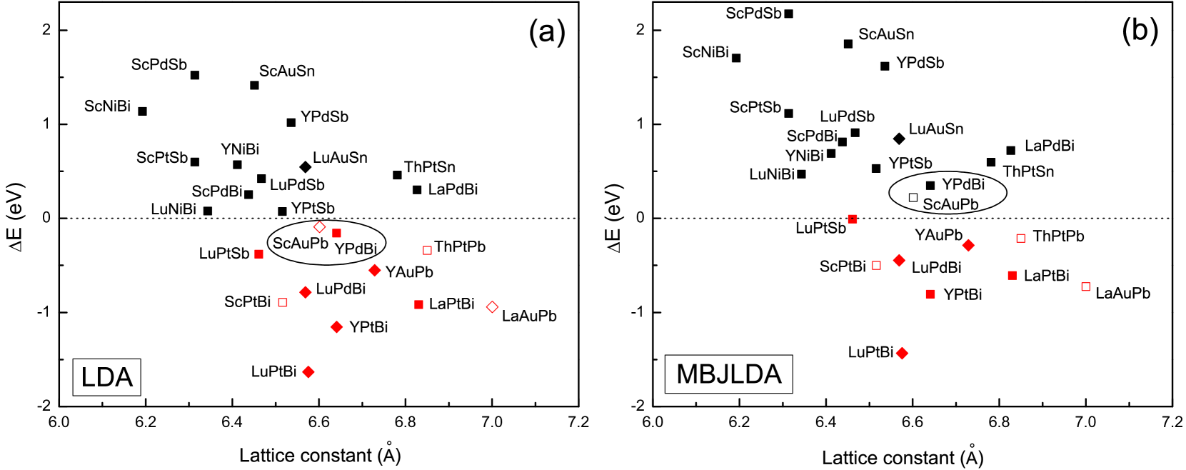
The band topology calculated by first-principles method is sensitive to the exchange-correlation potential [34,99]. Hence, different potentials should be used to explore the topological nature. The recently developed semilocal MBDLDA potential is believed to be better suited for calculating the topological band structure [34,99]. As shown in Fig. 5, the topologically nontrivial and trivial phases are located below and above the horizontal line, respectively. One can see that the topological phases of ScAuPb and YPdBi change by using different exchange-correlation potentials.
Recently, there have appeared a few experimental works about the electronic structures, transport properties, and topological phenomena of ternary half-Heusler compounds [100–104]. Since a large number of materials with half-Heusler structure possess additional properties such as magnetism [105] and superconductivity [106], the combination of the predicted topological order with ferromagnetic order and/or superconductive order may provide an exciting platform for novel quantum devices.
3.4.2 Chalcopyrite
The crystal structure of ternary chalcopyrite compounds is described by the space group (No. 122) with body-centered tetragonal structure. The chemical formula of these materials is , which can be regarded as a superlattice of two cubic zinc-blende unit cells and the A and B cations are ordered on the two different sites. Since the overall structural similarity between the ternary chalcopyrites and binary zinc-blende analogs, the electronic structures of the former one are expected to closely resemble that of latter one. Therefore, some of the chalcopyrite compounds may have the same topological class with the 3DTI HgTe.
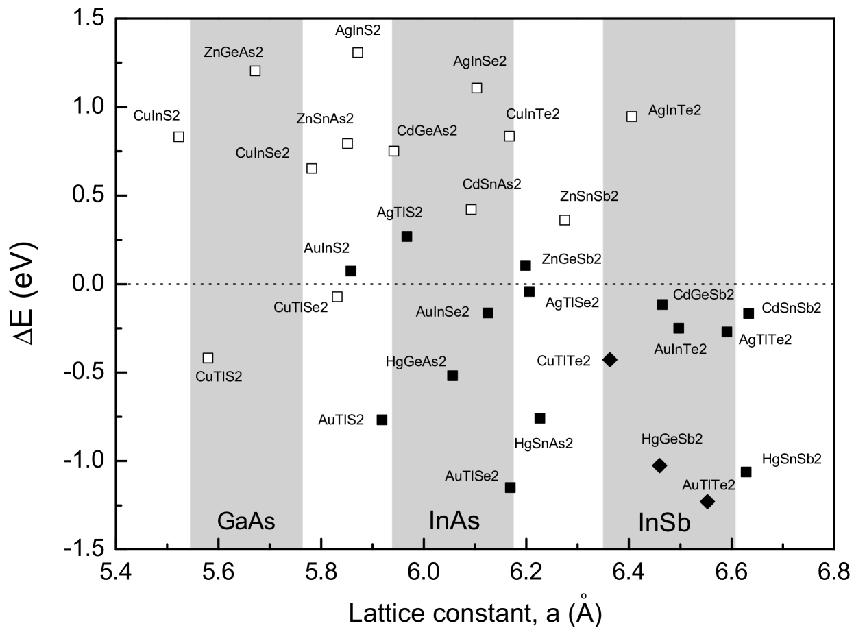
Feng et al. [42] predicted that a large number of chalcopyrite compounds can realize the topological insulating phase by exploiting adiabatic continuity of band structures and direct evaluation of the topological invariants. Comparing with other 3DTI with cubic symmetry, a seeming advantage in chalcopyrite compounds is that topologically nontrivial state can be formed in their native states without any external strain. This is because the AB cation ordering and additional structural modifications explicitly break the cubic symmetry. In chalcopyrite compounds, the band inversion strength is redefined as the energy difference between the -orbital originated states and the VBM at the point. Figure 6 shows the band topology of the chalcopyrite family of the I-III-VI2 compounds (I = Cu, Ag, Au; III = In, Tl; V = S, Se, Te), as well as the II-IV-V2 compounds (II = Zn, Cd, Hg; IV = Ge, Sn; V = As, Sb). One can see that there are a large number of topologically nontrivial materials. More importantly, many chalcopyrite topological insulators have a close lattice matching to several mainstream semiconductors, which is essential for a smooth integration into current semiconductor technology. The diverse physical properties of chalcopyrite semiconductors [108–111] make them appealing candidates for novel quantum devices.
3.4.3 Thallium-based chalcogenides
Thallium-based chalcogenides are narrow band-gap semiconductors with rhombohedral structure described by space group Rm (No. 166). The elemental composition of these materials is Tl ( = Bi, Sb and = S, Se, Te), which can be regarded as a sequence of hexagonally close-packed layers with the order of -Tl-Y-X-Y-. In contrast to Bi2Se3 family, the Tl are not layered compounds because each Tl or X atomic layer is sandwiched by two Y atomic layers and every two atomic layers are coupled by strong covalent bonds. As a consequence, the surface electronic structure is sensitive to surface relaxations and different terminations.
Although the identification of topologically nontrivial phase in these compounds is more complex than that of Bi2Se3 family, several first-principles studies have predicted that TlSbTe2, TlSbSe2, TlBiTe2, and TlBiSe2 are 3DTI [112–114]. The single Dirac cone surface state of TlBiTe2, and TlBiSe2 have been confirmed by ARPES measurements [115–118].
3.5 3DTI in quaternary compounds
The search for 3DTI has already been extended to quaternary I2-II-IV-VI4 compounds [133,134]. These materials are described by space group I2m (No. 121) with body-centered tetragonal structure. Structurally, quaternary I2-II-IV-VI4 compounds can be viewed as the subcompounds derived from chalcopyrite I-III-VI2 compounds by mutating two group-III cations to one group-II and one group-IV cations. Because of the structural similarity, the band topology of these compounds is expected to be nontrivial in analogy to that of chalcopyrite 3DTI [42]. Based on first-principles calculations, Chen et al. [134] and Wang et al. [133] predicted that a number of I2-II-IV-VI4 compounds are indeed topologically nontrivial materials. More importantly, the electronic properties of these compounds can be better altered because of the enhanced chemical and structural degrees of freedom. For example, the nontrivial band-gaps can be further increased in Ag2HgPbSe4 (0.047 eV) and Cu2ZnGeSe4 (0.069 eV), which are larger than the band-gaps in strained HgTe and some of chalcopyrite compounds.
| Coupounds | Bravais lattice | Space group (No.) | Band gap (eV) | Strain | Theory works | Experiment works |
| -Sn | fcc | Fdm (227) | zero[17] | yes | [17] | – |
| Sb | rho | Rm (166) | semimetal[17] | no | [17,37] | [51,52] |
| Bi1-xSbx | rho | – | 0.03 (=0.18)[17] | no | [17,26,27] | [52,55–57] |
| Bi2Se3 | rho | Rm (166) | 0.30[66] | no | [35,66] | [58] |
| Bi2Te3 | rho | Rm (166) | 0.12[66] | no | [35,66] | [59,60] |
| Sb2Te3 | rho | Rm (166) | 0.17[66] | no | [35,66] | [60] |
| HgTe | fcc | F3m (216) | zero[17] | yes | [17] | [72] |
| -HgS | fcc | F3m (216) | 0.042[73] | no | [73] | – |
| InSb | fcc | F3m (216) | zero[75] | yes | [75] | – |
| -Ag2Te | fcc | P21/c (14) | 0.08[76] | no | [76] | – |
| Sr2Pb | orc | Pnma (62) | 0.05[77] | yes | [77] | – |
| -GaS | hex | P63/mmc (194) | 0.025[78] | yes | [78] | – |
| -GaSe | hex | Pm2 (187) | 0.135[78] | yes | [78] | – |
| Na3Bi | hex | P63/mmc (194) | 0.006[79] | yes | [79] | – |
| K3Bi | hex | P63/mmc (194) | – | yes | [79] | – |
| Rb3Bi | hex | P63/mmc (194) | – | yes | [79] | – |
| Bi2Te2S | rho | Rm (166) | 0.28[89] | no | [88,89] | – |
| Bi2Te2Se | rho | Rm (166) | 0.28[89] | no | [88–90] | [86,87,90,91,94] |
| Bi2Se2Te | rho | Rm (166) | 0.17[89] | no | [89,90] | [90] |
| Sb2Te2S | rho | Rm (166) | 0.29[88] | no | [88] | – |
| Sb2Te2Se | rho | Rm (166) | 0.34[88] | no | [88] | – |
| Bi2Te1.5S1.5 | rho | – | 0.2[90] | no | [90] | [90] |
| Bi2Te1.6S1.4 | rho | – | 0.2[91] | no | – | [91] |
| Bi2-xSbxTe3 | rho | – | – | no | [93] | [92,93] |
| Bi2-xSbxTe3-ySey | rho | – | – | no | – | [94–96] |
| half-Heusler (see Fig. 5) | fcc | F3m (216) | zero[33,34] | yes | [33,34,97–99] | [100–104] |
| Li2AgSb | fcc | F3m (216) | zero[107] | yes | [107] | – |
| chalphyrite (see Fig. 6) | bct | I2d (122) | 0.010.14[42] | no | [42] | – |
| TlBiSe2 | rho | Rm (166) | 0.2[118] | no | [112–114] | [115–118] |
| TlBiTe2 | rho | Rm (166) | semimetal[118] | no | [112–114] | [118] |
| TlSbSe2 | rho | Rm (166) | 0.14[113] | no | [112–114] | – |
| TlSbTe2 | rho | Rm (166) | 0.05[113] | no | [112–114] | – |
| LaBiTe3 | rho | Rm (166) | 0.12[119] | no | [119] | – |
| CeOs4As12 | bcc | Im (204) | zero[120] | yes | [120] | – |
| CeOs4Sb12 | bcc | Im (204) | zero[120] | yes | [120] | – |
| Ca3NBi | cub | Pmm (221) | 0.03[121] | yes | [121] | – |
| Sr3NBi | cub | Pmm (221) | – | yes | [121] | – |
| Ba3NBi | cub | Pmm (221) | – | yes | [121] | – |
| CsSnCl3 | cub | Pmm (221) | 0.111[122] | yes | [122] | – |
| CsPbCl3 | cub | Pmm (221) | 0.354[122] | yes | [122] | – |
| CsGeBr3 | cub | Pmm (221) | 0.026[122] | yes | [122] | – |
| CsSnBr3 | cub | Pmm (221) | 0.099[122] | yes | [122] | – |
| CsPbBr3 | cub | Pmm (221) | 0.120[122] | yes | [122] | – |
| CsSnI3 | cub | Pmm (221) | 0.169[122] | yes | [122] | – |
| LiAgSe | hex | P63/mmc (194) | 0.001[123] | yes | [123] | – |
| LiAuSe | hex | P63/mmc (194) | 0.050[123] | yes | [123] | – |
| LiAuTe | hex | P63/mmc (194) | – | yes | [123] | – |
| NaAgSe | hex | P63/mmc (194) | 0.010[123] | yes | [123] | – |
| NaAgTe | hex | P63/mmc (194) | 0.003[123] | yes | [123] | – |
| NaAuSe | hex | P63/mmc (194) | 0.015[123] | yes | [123] | – |
| NaAuTe | hex | P63/mmc (194) | 0.030[123] | yes | [123] | – |
| KAuTe | hex | P63/mmc (194) | – | yes | [123] | – |
| LiHgAs | hex | P63/mmc (194) | – | yes | [123] | – |
| LiHgSb | hex | P63/mmc (194) | – | yes | [123] | – |
| BiTeI | hex | P3m1 (156) | – | yes | [124] | – |
| Ge2Sb2Te5(Petrov sequence) | hex | Pm1 (164) | 0.1[125] | no | [125] | – |
| Ge2Sb2Te5(KH sequence) | hex | Pm1 (164) | – | no | [126,127] | – |
| PbBi2Se4 | rho | Rm (166) | 0.40[128] | no | [128,131,132] | [131,132] |
| PbBi2Te4 | rho | Rm (166) | 0.23[129] | no | [129,131,132] | [129–132] |
| Pb(Bi1-xSbx)2Te4 | rho | – | – | no | – | [130] |
| GeBi2Te4 | rho | Rm (166) | – | no | [131,132] | [131,132] |
| GeSb2Te4 | rho | Rm (166) | – | no | [131,132] | [131,132] |
| SnBi2Te4 | rho | Rm (166) | – | no | [131,132] | [131,132] |
| SnSb2Te4 | rho | Rm (166) | – | no | [131,132] | [131,132] |
| PbSb2Te4 | rho | Rm (166) | – | no | [131,132] | [131,132] |
| GeBi4Te7 | hex | Pm1 (164) | – | no | [131,132] | [131,132] |
| GeSb4Te7 | hex | Pm1 (164) | – | no | [131,132] | [131,132] |
| SnBi4Te7 | hex | Pm1 (164) | – | no | [131,132] | [131,132] |
| SnSb4Te7 | hex | Pm1 (164) | – | no | [131,132] | [131,132] |
| PbBi4Se7 | hex | Pm1 (164) | – | no | [131,132] | [131,132] |
| PbBi4Te7 | hex | Pm1 (164) | – | no | [131,132] | [131,132] |
| PbSb4Te7 | hex | Pm1 (164) | – | no | [131,132] | [131,132] |
| GeBi6Te10 | rho | Rm (166) | – | no | [131] | [131] |
| SnBi6Te10 | rho | Rm (166) | – | no | [131] | [131] |
| PbBi6Te10 | rho | Rm (166) | – | no | [131] | [131] |
| Cu3SbS4 | bct | I2m (121) | 0.042[133] | no | [133] | – |
| Cu2ZnGeSe4 | bct | I2m (121) | 0.069[133] | no | [133] | – |
| Cu2ZnSnSe4 | bct | I2m (121) | 0.056[133] | no | [133] | – |
| Cu2CdGeSe4 | bct | I2m (121) | 0.003[133] | no | [133] | – |
| Cu2CdSnSe4 | bct | I2m (121) | 0.003[133] | no | [133] | – |
| Cu2HgGeSe4 | bct | I2m (121) | 0.006[133] | no | [133] | – |
| Cu2HgSnSe4 | bct | I2m (121) | 0.007[133] | no | [133] | – |
| Cu2CdSnS4 | bct | I2m (121) | 0.033[133] | no | [133] | – |
| Cu2HgSnS4 | bct | I2m (121) | 0.060[133] | no | [133] | – |
| Ag2HgPbSe4 | bct | I2m (121) | 0.047[134] | no | [134] | – |
| Ag2CdPbTe4 | bct | I2m (121) | – | no | [134] | – |
| Cu2HgPbSe4 | bct | I2m (121) | – | no | [134] | – |
| Cu2CdPbSe4 | bct | I2m (121) | – | no | [134] | – |
4 Conclusion and outlook
Since the potential applications in spintronic field and quantum computation, 3DTI has no doubt become topic of interest in the fields of condensed matter physics and material science. Thousands of scientific colleagues are attracted by its exotic quantum phenomena, pushing this field in a rapid pace. Similar to other stages of development in the history of condensed matter physics, for example the QH effect, the emergence of high quality samples is of crucial importance. For this purpose, this paper reviews the recent progress of materials realization in 3DTI.
Based on topological band theory [18,19], the first-principles calculation plays a pivotal role in the prediction of 3DTI host materials. We have introduced four methods of searching for new 3DTI, including surface state electronic structure, adiabatic continuity band transformation, band inversion picture, and topological invariants. None of these methods is solely used in present literatures, but two or more of them are usually combined together to predict topologically nontrivial materials. To date, many materials have been predicted to be 3DTI (see Table LABEL:tab1). Some of them have been confirmed by experiments via the ARPES measurements of surface Dirac electronic structure. The most favorable materials are thus the Bi2Se3 family, which have been extensively studied from bulk to thinfilm [58–71]. But remarkably conducting bulk state even in high quality sample blocks further studies of the surface transport. For decreasing the bulk carrier concentration, the pseudo-binary compound derived from Bi2Se3 family, for example Bi2Te2Se, is found to be new class of 3DTI with much larger bulk resistivity [86–94]. The theoretical prediction of 3DTI was also extended to ternary and quaternary compounds, but there are rare experimental reports about these compounds mainly because of the difficulties in their synthesis and growth.
We propose several interesting and valuable directions in the further work. (i) Among the present known 3DTI host materials, there does not exist a unique one which can sufficiently meet various requirements in experimental observations. Therefore, searching for new 3DTI host materials, particularly for those with simpler surface electronic structure and easier synthetic and growing condition, is still needed. This should be a central task in this rapidly developing field. (ii) Although the present 3DTI host materials are often discussed in the context of the non-interacting band theory, the materials realization of topological Mott insulator [135,136] and topological Kondo insulator [137,138] with strong electron-electron interaction should also be taken into account. Furthermore, the topological order affected by disorder, i.e., topological Anderson insulator [139–141], is interesting and needs to be thoroughly studied. (iii) The realization of the quantum anomalous Hall effect and topological superconductor is also a frontier direction. For quantum anomalous Hall effect, some theoretical models were proposed by means of magnetic doping in the film or surface of 3DTI [142–147], but they have not been reproduced by current experiments. For topological superconductor, one expects to realize it by constructing proper interface between 3DTI and conventional superconductors due to the proximity effect [18,148]. In addition, a mysterious particle obeyed non-Abelian statistics, the Majorana fermion, could be detected in the interface and it will be hopefully utilized in the topological quantum computations.
The authors were supported by National Basic Research Program of China (973 Program Grants No. 2011CBA00100) and National Natural Science Foundation of China (Grants No. 10974231 and 11174337).
1 Wen X G. Topological orders and edge excitations in fractional quantum Hall states. Adv Phys, 1995, 44: 405–473 \REF2 Thouless D J, Kohmoto M, Nightingale M P, Nijs M d. Quantized hall conductance in a two-dimensional periodic potential. Phys Rev Lett, 1982, 49: 405–408 \REF3 Klitzing K v, Dorda G, Pepper M. New method for high-accuracy determination of the fine-structure constant based on quantized Hall resistance. Phys Rev Lett, 1980, 45: 494–497 \REF4 Bernevig B A, Zhang S C. Quantum spin Hall effect. Phys Rev Lett, 2006, 96: 106802 \REF5 Kane C L, Mele E J. A new spin on the insulating state. Science, 2006, 314: 1692–1693 \REF6 Kane C L, Mele E J. Quantum spin Hall effect in graphene. Phys Rev Lett, 2005, 95: 226801 \REF7 Kane C L, Mele E J. Z2 topological order and the quantum spin Hall effect. Phys Rev Lett, 2005, 95: 146802 \REF8 Kohn W. Theory of the insulating state. Phys Rev, 1964, 133: A171–A181 \REF9 Yao Y G, Ye F, Qi X L, et al. Spin-orbit gap of graphene: First-principles calculations. Phys Rev B, 2007, 75: 041401 \REF10 Huertas-Hernando D, Guinea F, Brataas A. Spin-orbit coupling in curved graphene, fullerenes, nanotubes, and nanotube caps. Phys Rev B, 2006, 74: 155426 \REF11 Min H, Hill J E, Sinitsyn N A, et al. Intrinsic and Rashba spin-orbit interactions in graphene sheets. Phys Rev B, 2006, 74: 165310 \REF12 Bernevig B A, Hughes T L, Zhang S C. Quantum spin Hall effect and topological phase transition in HgTe quantum wells. Science, 2006, 314: 1757–1761 \REF13 König M, Wiedmann S, Brüne C, et al. Quantum spin Hall insulator state in HgTe quantum wells. Science, 2006, 318: 766-770 \REF14 Fu L, Kane C L, Mele E J. Topological insulators in three dimensions. Phys Rev Lett, 2007, 98: 106803 \REF15 Moore J E, Balents L. Topological invariants of time-reversal-invariant band structures. Phys Rev B, 2007, 75: 121306 \REF16 Roy R. Topological phases and the quantum spin Hall effect in three dimensions. Phys Rev B, 2009, 79: 195322 \REF17 Fu L, Kane C L. Topological insulators with inversion symmetry. Phys Rev B, 2007, 76: 045302 \REF18 Qi X L, Zhang S C. Topological insulators and superconductors. Rev Mod Phys, 2011, 83: 1057–1110 \REF19 Qi X L, Zhang S C. The quantum spin Hall effect and topological insulators. Physics Today, 2010, 63: 33–38 \REF20 Hasan M Z, Kane C L. Colloquium : Topological insulators. Rev Mod Phys, 2010, 82: 3045–3067 \REF21 Hasan M Z, Moore J E. Three-dimensional topological insulators. Ann Rev Cond Matter Phys, 2011, 2: 55–78 \REF22 Moore J E. The birth of topological insulators. Nature (London), 2010, 464: 194–198 \REF23 Brumfiel G, Topological insulators: Star material. Nature (London), 2010, 466: 310–311 \REF24 DiVincenzo D P, Mele E J. Self-consistent effective-mass theory for intralayer screening in graphite intercalation compounds. Phys Rev B, 1984, 29: 1685–1694 \REF25 Semenoff G W. Condensed-matter simulation of a three-dimensional anomaly. Phys Rev Lett, 1984, 53: 2449–2452 \REF26 Appelbaum Joel A, Hamann D R. The electronic structure of solid surfaces. Rev Mod Phys, 1976, 48: 479–496 \REF27 Hoffmann R. A chemical and theoretical way to look at bonding on surfaces. Rev Mod Phys, 1988, 60: 601–628 \REF28 Hoffmann R. Solids and surfaces: a chemist’s view of bonding in extended structures. New York: VCH Publishers, 1988. \REF29 Liu C C, Feng W X, Yao Y G. Quantum spin Hall effect in silicene and two-dimensional germanium. Phys Rev Lett, 2011, 107: 076802 \REF30 Teo J C Y, Fu L, Kane C L. Surface states and topological invariants in three-dimensional topological insulators: Application to Bi1-xSbx. Phys Rev B, 2008, 78: 045426 \REF31 Zhang H J, Liu C X, Qi X L, et al. Electronic structures and surface states of the topological insulator Bi1-xSbx. Phys Rev B, 2009, 80: 085307 \REF32 Delin A, Klüner T. Excitation spectra and ground-state properties from density-functional theory for the inverted band-structure systems -HgS, HgSe, and HgTe. Phys Rev B, 2002, 66: 035117. \REF33 Xiao D, Yao Y G, Feng W X, et al. Half-Heusler compounds as a new class of three-dimensional topological insulators. Phys Rev Lett, 2010, 105: 096404 \REF34 Feng W X, Xiao D, Zhang Y, et al. Half-Heusler topological insulators: A first-principles study with the Tran-Blaha modified Becke-Johnson density functional. Phys Rev B, 2010, 82: 235121 \REF35 Zhang H J, Liu C X, Qi X L, et al. Topological insulators in Bi2Se3, Bi2Te3 and Sb2Te3 with a single Dirac cone on the surface. Nature Phys, 2009, 5: 438–442 \REF36 Zhang X, Zhang H J, Wang J, et al. Actinide topological insulator materials with strong interaction. Science, 2012, 335: 1464–1466 \REF37 Fukui T, Hatsugai Y. Quantum spin Hall effect in three dimensional materials: Lattice computation of Z2 topological invariants and its application to Bi and Sb. J. Phys. Soc. Japan, 2007, 76: 053702 \REF38 Feng W X, Wen J, Zhou J J, et al. First-principles calculation of Z2 topological invariants within the FP-LAPW formalism. Comp Phys Comm, 2012, 183: 1849–1859 \REF39 Fu L, Kane C L. Time reversal polarization and a Z2 adiabatic spin pump. Phys. Rev. B, 2006, 74: 195312 \REF40 King-Smith R D, Vanderbilt D. Theory of polarization of crystalline solids. Phys Rev B, 1993, 47: 1651–1654 \REF41 Resta R. Macroscopic polarization in crystalline dielectrics: the gemetric phase approach. Rev Mod Phys, 1994, 66: 899–915 \REF42 Feng W X, Xiao D, Ding J, et al. Three-dimensional topological insulators in I-III-VI2 and II-IV-V2 chalcopyrite semiconductors. Phys Rev Lett, 2011, 106: 016402 \REF43 Soluyanov A A, Vanderbilt D. Computing topological invariants without inversion symmetry. Phys Rev B, 2011,83: 235401 \REF44 Yu R, Qi X L, Bernevig A, et al. Equivalent expression of Z2 topological invariant for band insulators using the non-Abelian Berry connection. Phys Rev B, 2011, 84: 075119 \REF45 Singh D J. Planewaves, Pseudopotentials and the LAPW Method. Boston: Kluwer Academic, 1994. \REF46 Tran F, Blaha P. Accurate band gaps of semiconductors and insulators with a semilocal exchange-correlation potential. Phys Rev Lett, 2009, 102: 226401 \REF47 Blaha P, Schwarz K, Madsen G, et al. Wien2k, an augmented plane wave plus local orbitals program for calculating crystal properties. Austria: Vienna University of Technology, Vienna, 2001. \REF48 Groves S, Paul W. Band structure of gray tin. Phys Rev Lett, 1963, 11: 194–196 \REF49 Chelikowsky J R, Cohen M L. Nonlocal pseudopotential calculations for the electronic structure of eleven diamond and zinc-blende semiconductors. Phys Rev B, 1976, 14: 556–582 \REF50 Perdew J P, Burke K, Ernzerhof M. Generalized gradient approximation made simple. Phys Rev Lett, 1996, 77: 3865–3868 \REF51 Hsieh D, Wray L, Qian D, et al. Direct observation of spin-polarized surface states in the parent compound of a topological insulator using spin- and angle-resolved photoemission spectroscopy in a Mott-polarimetry mode. New J Phys, 2010, 12: 125001 \REF52 Hsieh D, Xia Y, Wray L, et al. Observation of unconventional quantum spin textures in topological insulators. Science, 2009, 323: 919–922 \REF53 Lerner L S, Cuff K F, Williams L R. Energy-band parameters and relative band-edge motions in the Bi-Sb alloy system near the semimetal semiconductor transition. Rev Mod Phys, 1968, 40: 770–775 \REF54 Liu Y, Allen R E. Electronic structure of the semimetals Bi and Sb. Phys Rev B, 1995, 52: 1566–1577 \REF55 Hsieh D, Qian D, Wray L, et al. A topological Dirac insulator in a quantum spin Hall phase. Nature (London) 2008, 452: 970–974 \REF56 Guo H, Sugawara K, Takayama A, et al. Evolution of surface states in Bi1-xSbx alloys across the topological phase transition. Phys Rev B, 2011, 83: 201104 \REF57 Nishide A, Taskin A A, Takeichi Y, et al. Direct mapping of the spin-filtered surface bands of a three-dimensional quantum spin Hall insulator. Phys Rev B, 2010, 81: 041309 \REF58 Xia Y, Qian D, Hsieh D, et al. Observation of a large-gap topological-insulator class with a single Dirac cone on the surface. Nature Phys. 2009, 5: 398–402 \REF59 Chen Y L, Analytis J G, Chu J H, et al. Experimental realization of a three-dimensional topological insulator, Bi2Te3. Science 2009, 325: 178–180 \REF60 Hsieh D, Xia Y, Qian D, et al. Observation of time-reversal-protected single-Dirac-cone topological-insulator states in Bi2Te3 and Sb2Te3. Phys Rev Lett, 2009, 103: 146401 \REF61 Zhang T, Cheng P, Chen X, et al. Experimental demonstration of topological surface states protected by time-reversal symmetry. Phys Rev Lett, 2009, 103: 266803 \REF62 Chen Y L, Chu J H, Analytis J G, et al. Massive Dirac fermion on the surface of a magnetically doped topological insulator. Science 2010, 329: 659–662 \REF63 Hsieh D, Xia Y, Qian D, et al. A tunable topological insulator in the spin helical Dirac transport regime. Nature (London) 2009, 460: 1101–1105 \REF64 Kuroda K, Arita M, Miyamoto K, et al. Hexagonally deformed Fermi surface of the 3D topological insulator Bi2Se3. Phys Rev Lett, 2010, 105: 076802 \REF65 Zhang J L, Zhang S J, Weng H M, et al. Pressure-induced superconductivity in topological parent compound Bi2Te3. PNAS, 2011, 108: 24–28 \REF66 Zhang W, Yu R, Zhang H J, et al. First-principles studies of the three-dimensional strong topological insulators Bi2Te3, Bi2Se3 and Sb2Te3. New J Phys, 2010, 12: 065013 \REF67 Park K, Heremans J J, Scarola V W, et al. Robustness of topologically protected surface states in layering of Bi2Te3 thin films. Phys Rev Lett, 2010, 105: 186801 \REF68 Yu R, Zhang W, Zhang H J, et al. Quantized anomalous Hall effect in magnetic topological insulators. Science, 2010, 329: 61–64 \REF69 Liu C X, Qi X L, Zhang H J, et al. Model Hamiltonian for topological insulators. Phys Rev B, 2010, 82: 045122 \REF70 Liu C X, Zhang H J, Yan B H, et al. Oscillatory crossover from two-dimensional to three-dimensional topological insulators. Phys Rev B, 2010, 81: 041307 \REF71 Song J H, Jin H, Freeman A J. Interfacial Dirac cones from alternating topological invariant superlattice structures of Bi2Se3. Phys Rev Lett, 2010, 105: 096403 \REF72 Brüne C, Liu C X, Novik E G, et al. Quantum Hall effect from the topological surface states of strained bulk HgTe. Phys Rev Lett, 2011, 106: 126803 \REF73 Virot F, Hayn R, Richter M, et al. Metacinnabar (-HgS): A strong 3D topological insulator with highly anisotropic surface states. Phys Rev Lett, 2011, 106: 236806 \REF74 Madelung O. Semiconductors: Data handbook. Berlin: Springer, 2004. \REF75 Feng W X, Zhu W G, Weitering H H, et al. Strain tuning of topological band order in cubic semiconductors. Phys Rev B, 2012, 85: 195114 \REF76 Zhang W, Yu R, Feng W X, et al. Topological aspect and quantum magnetoresistance of -Ag2Te. Phys Rev Lett, 2011, 106: 156808 \REF77 Sun Y, Chen X Q, Franchini C, et al. Strain-driven onset of nontrivial topological insulating states in Zintl Sr2X compounds (X = Pb, Sn). Phys Rev B, 2011, 84: 165127 \REF78 Zhu Z Y, Cheng Y C, Schwingenschlögl U. Topological phase transition in layered GaS and GaSe. Phys Rev Lett, 2012, 108: 266805 \REF79 Wang Z, Sun Y, Chen X Q, et al. Dirac semimetal and topological phase transitions in A3Bi (A = Na, K, Rb). Phys Rev B, 2012, 85: 195320 \REF80 Hor Y S, Richardella A, Roushan P, et al. p-type Bi2Se3 for topological insulator and low-temperature thermoelectric applications. Phys Rev B, 2009, 79: 195208 \REF81 Checkelsky J G, Hor Y S, Liu M H, et al. Quantum interference in macroscopic crystals of nonmetallic Bi2Se3. Phys Rev Lett, 2009, 103: 246601 \REF82 Analytis J G, Chu J H, Chen Y L, et al. Bulk Fermi surface coexistence with Dirac surface state in Bi2Se3: A comparison of photoemission and Shubnikov-de Haas measurements. Phys Rev B, 2010, 81: 205407 \REF83 Chen J, Qin H J, Yang F, et al. Gate-voltage control of chemical potential and weak antilocalization in Bi2Se3. Phys Rev Lett, 2010, 105: 176602 \REF84 Chen J, He X Y, Wu K H, et al. Tunable surface conductivity in Bi2Se3 revealed in diffusive electron transport. Phys Rev B, 2011, 83: 241304 \REF85 Checkelsky J G, Hor Y S, Cava R J, et al. Bulk band gap and surface state conduction observed in voltage-tuned crystals of the topological insulator Bi2Se3. Phys Rev Lett, 2011, 106: 196801 \REF86 Ren Z, Taskin A A, Sasaki S, et al. Large bulk resistivity and surface quantum oscillations in the topological insulator Bi2Te2Se. Phys Rev B, 2010, 82: 241306 \REF87 Xiong J, Petersen A C, Qu D X, et al. Quantum oscillations in a topological insulator Bi2Te2Se with large bulk resistivity (6 cm). Physica E, 2012, 44: 917–920 \REF88 Lin H, Das T, Wray L A, et al. An isolated Dirac cone on the surface of ternary tetradymite-like topological insulators. New J Phys, 2011, 13: 095005 \REF89 Wang L L, Johnson D D. Ternary tetradymite compounds as topological insulators. Phys Rev B, 2011, 83: 241309 \REF90 Neupane M, Xu S Y, Wray L A, et al. Topological surface states and Dirac point tuning in ternary topological insulators. Phys Rev B, 2012, 85: 235406 \REF91 Ji H W, Allred J M, Fuccillo M K, et al. Bi2Te1.6S1.4: A topological insulator in the tetradymite family. Phys Rev B, 2012, 85: 201103 \REF92 Zhang J S, Chang C Z, Zhang Z C, et al. Band structure engineering in (Bi1-xSbx)2Te3 ternary topological insulators. Nature Commun, 2011, 2: 574 \REF93 Kong D S, Chen Y L, Cha J J, et al. Ambipolar field effect in the ternary topological insulator (BixSb1-x)2Te3 by composition tuning. Nature Nanotech, 2011, 6: 705–709 \REF94 Arakane T, Sato T, Souma S, et al. Tunable Dirac cone in the topological insulator Bi2-xSbxTe3-ySey. Nature Commun, 2012, 3: 636 \REF95 Ren Z, Taskin A A, Sasaki S, et al. Optimizing Bi2-xSbxTe3-ySey solid solutions to approach the intrinsic topological insulator regime. Phys Rev B, 2011, 84: 165311 \REF96 Taskin A A, Ren Z, Sasaki S, et al. Observation of Dirac holes and electrons in a topological insulator. Phys Rev Lett, 2011, 107: 016801 \REF97 Chadov S, Qi X L, Kübler J, et al. Tunable multifunctional topological insulators in ternary Heusler compounds. Nature Mater, 2010, 9: 541–545 \REF98 Lin H, Wray L A, Xia Y, et al. Half-Heusler ternary compounds as new multifunctional experimental platforms for topological quantum phenomena. Nature Mater. 2010, 9: 546–549 \REF99 Al-Sawai W, Lin H, Markiewicz R S, et al. Topological electronic structure in half-Heusler topological insulators. Phys Rev B, 2010, 82: 125208 \REF100 Gofryk K, Kaczorowski D, Plackowski T, et al. Magnetic and transport properties of rare-earth-based half-Heusler phases RPdBi: Prospective systems for topological quantum phenomena. Phys Rev B, 2011, 84: 035208 \REF101 Liu C, Lee Y, Kondo T, et al. Metallic surface electronic state in half-Heusler compounds RPtBi (R = Lu, Dy, Gd). Phys Rev B, 2011, 83: 205133 \REF102 Butch N P, Syers P, Kirshenbaum K, et al. Superconductivity in the topological semimetal YPtBi. Phys Rev B, 2011 84: 220504 \REF103 Shekhar C, Ouardi S, Fecher G H, et al. Electronic structure and linear magnetoresistance of the gapless topological insulator PtLuSb. Appl Phys Lett, 2012, 100: 252109 \REF104 Miyawaki T, Sugimoto N, Fukatani N, et al. Structural and electrical properties of half-Heusler La-Pt-Bi thin films grown by 3-source magnetron co-sputtering. J Appl Phys, 2012, 111: 07E327 \REF105 Canfield P C, Thompson J D, Beyermann W P, et al. Magnetism and heavy fermion-like behavior in the RBiPt series. J Appl Phys, 1991, 70: 5800–5802 \REF106 Goll G, Marz M, Hamann A, et al. Thermodynamic and transport properties of the non-centrosymmetric superconductor LaBiPt. Physica B, 2008, 403: 1065–1067 \REF107 Lin H, Wray L A, Xia Y, et al. Single-Dirac-cone Z2 topological insulator phases in distorted Li2AgSb-class and related quantum critical Li-based spin-orbit compounds. E-print at arXiv:1004.0999 \REF108 Shay J L, Wernick J H. Ternary chalcopyrite semiconductors: Growth, electronic properties and applications. Oxford: Pergamon Press, 1975. \REF109 Medvedkin G A, Ishibashi T, Nishi T, et al. Room temperature ferromagnetism in novel diluted magnetic semiconductor (Cd1-xMnx)GeP2. Jpn J Appl Phys, 2000, 39: L949–L951 \REF110 Cho S, Choi S, Cha G B, et al. Room-temperature ferromagnetism in (Zn1-xMnx)GeP2 semiconductors. Phys Rev Lett, 2002, 88: 257203 \REF111 Erwin S C, Žutić I. Tailoring ferromagnetic chalcopyrites. Nature Mater, 2004, 3: 410–414 \REF112 Lin H, Markiewicz R S, Wray L A, et al. Single-Dirac-cone topological surface states in the TlBiSe2 class of topological semiconductors. Phys Rev Lett, 2010, 105: 036404 \REF113 Yan B H, Liu C X, Zhang H J, et al. Theoretical prediction of topological insulators in thallium-based III-V-VI2 ternary chalcogenides. Europhys Lett, 2010, 90: 37002 \REF114 Eremeev S V, Bihlmayer G, Vergniory M, et al. Ab initio electronic structure of thallium-based topological insulators. Phys Rev B, 2011, 83: 205129 \REF115 Kuroda K, Ye M, Kimura A, et al. Experimental realization of a three-dimensional topological insulator phase in ternary chalcogenide TlBiSe2. Phys Rev Lett, 2010, 105: 146801 \REF116 Sato T, Segawa K, Guo H, et al. Direct evidence for the Dirac-cone topological surface states in the ternary chalcogenide TlBiSe2. Phys Rev Lett, 2010, 105: 136802 \REF117 Xu S Y, Xia Y, Wray L A, et al. Topological phase transition and texture inversion in a tunable topological insulator. Science, 2011, 332: 560–564 \REF118 Chen Y L, Liu Z K, Analytis J G, et al. Single Dirac cone topological surface state and unusual thermoelectric property of compounds from a new topological insulator family. Phys Rev Lett, 2010, 105: 266401 \REF119 Yan B H, Zhang H J, Liu C X, et al. Theoretical prediction of topological insulator in ternary rare earth chalcogenides. Phys Rev B, 2010, 82: 161108 \REF120 Yan B H, Müchler L, Qi X L, et al. Topological insulators in filled skutterudites. Phys Rev B, 2012, 85: 165125 \REF121 Sun Y, Chen X Q, Yunoki S, et al. New family of three-dimensional topological insulators with antiperovskite structure. Phys Rev Lett, 2010, 105: 216406 \REF122 Yang K, Setyawan W, Wang S D, et al. A search model for topological insulators with high-throughput robustness descriptors. Nature Mater, 2012, 11: 614–619 \REF123 Zhang H J, Chadov S, Müchler L, et al. Topological insulators in ternary compounds with a honeycomb lattice. Phys Rev Lett, 2011, 106: 156402 \REF124 Bahramy M S, Yang B J, Arita R, et al. Emergence of non-centrosymmetric topological insulating phase in BiTeI under pressure. Nature Commun, 2012, 3: 679 \REF125 Kim J, Kim J, Jhi S H. Prediction of topological insulating behavior in crystalline Ge-Sb-Te. Phys Rev B, 2010, 82: 201312 \REF126 Sa B S, Zhou J, Song Z T, et al. Pressure-induced topological insulating behavior in the ternary chalcogenide Ge2Sb2Te5. Phys Rev B, 2011, 84: 085130 \REF127 Sa B, Zhou J, Sun Z, et al. Strain-induced topological insulating behavior in ternary chalcogenide Ge2Sb2Te5. Europhys Lett, 2011, 97: 27003 \REF128 Jin H, Song J H, Freeman A J, et al. Candidates for topological insulators: Pb-based chalcogenide series. Phys Rev B, 2011, 83: 041202 \REF129 Kuroda K, Miyahara H, Ye M, et al. Experimental verification of PbBi2Te4 as a 3D topological insulator. Phys Rev Lett, 2012, 108: 206803 \REF130 Souma S, Eto K, Nomura M, et al. Topological surface states in lead-based ternary telluride Pb(Bi1-xSbx)2Te4. Phys Rev Lett, 2012, 108: 116801 \REF131 Eremeev S V, Landolt G, Menshchikova T V, et al. Atom-specific spin mapping and buried topological states in a homologous series of topological insulators. Nature Commun, 2012, 3: 635 \REF132 Xu S Y, Wray L A, Xia Y, et al. Discovery of several large families of topological insulator classes with backscattering-suppressed spin-polarized single-dirac-cone on the surface. E-print at arXiv:1007.5111 \REF133 Wang Y J, Lin H, Das T, et al. Topological insulators in the quaternary chalcogenide compounds and ternary famatinite compounds. New J Phys, 2011, 13: 085017 \REF134 Chen S Y, Gong X G, Duan C G, et al. Band structure engineering of multinary chalcogenide topological insulators. Phys Rev B, 2011, 83: 245202 \REF135 Raghu S, Qi X L, Honerkamp C, et al. Topological Mott insulators. Phys Rev Lett, 2008, 100: 156401 \REF136 Zhang Y, Ran Y, Vishwanath A. Topological insulators in three dimensions from spontaneous symmetry breaking. Phys Rev B, 2009, 79: 245331 \REF137 Dzero M, Sun K, Galitski V, et al. Topological Kondo insulators. Phys Rev Lett, 2010, 104: 106408 \REF138 Dzero M, Sun K, Coleman P, et al. Theory of topological Kondo insulators. Phys Rev B, 2012, 85: 045130 \REF139 Li J, Chu R L, Jain J K, et al. Topological Anderson insulator. Phys Rev Lett, 2009, 102: 136806 \REF140 Groth C W, Wimmer M, Akhmerov A R, et al. Theory of the topological Anderson insulator. Phys Rev Lett, 2009, 103: 196805 \REF141 Guo H M, Rosenberg G, Refael G, et al. Topological Anderson insulator in three dimensions. Phys Rev Lett, 2010, 105: 216601 \REF142 Haldane F D M. Model for a quantum Hall effect without landau levels: Condensed-matter realization of the “parity anomaly”. Phys Rev Lett, 1988, 61: 2015–2018 \REF143 Liu C X, Qi X L, Dai X, et al. Quantum anomalous Hall effect in Hg1-yMnyTe quantum wells. Phys Rev Lett, 2008, 101: 146802 \REF144 Yu R, Zhang W, Zhang H J, et al. Quantized anomalous Hall effect in magnetic topological insulators. Science, 2010, 329: 61–64 \REF145 Qiao Z H, Yang S Y A, Feng W X, et al. Quantum anomalous Hall effect in graphene from Rashba and exchange effects. Phys Rev B, 2010, 82: 161414 \REF146 Ding J, Qiao Z H, Feng W X, et al. Engineering quantum anomalous/valley Hall states in graphene via metal-atom adsorption: An ab-initio study. Phys Rev B, 2011, 84: 195444 \REF147 Zhang H J, Zhang X, Zhang S C. Quantum Anomalous Hall Effect in Magnetic Topological Insulator GdBiTe3. E-print at arXiv:1108.4857 \REF148 Fu L, Kane C L. Superconducting proximity effect and Majorana fermions at the surface of a topological insulator. Phys Rev Lett, 2008, 100: 096407