Electronic properties of the MoSWS2 heterojunction
Abstract
We study the electronic structure of a heterojunction made of two monolayers of MoS2 and WS2. Our first-principles density functional calculations show that, unlike in the homogeneous bilayers, the heterojunction has an optically active band-gap, smaller than the ones of MoS2 and WS2 single layers. We find that that the optically active states of the maximum valence and minimum conduction bands are localized on opposite monolayers, and thus the lowest energy electron-holes pairs are spatially separated. Our findings portrait the MoSWS2 bilayer as a prototypical example for band-gap engineering of atomically thin two-dimensional semiconducting heterostructures.
Engineering the electronic properties of semiconductors by using heterojunctions has been the central concept in semiconductor science and technology for 5 decades. Alferov ; Cardona-Yu With the advent of quantum wells, band-gap engineering of quasi-two dimensional semiconductors made it possible to observe a wealth of new physical phenomena, including the integer and fractional quantum Hall effects in modulation doping GaAs/GaAlAs,VK ; Tsui the condensation of both excitons in double GaAs quantum wells of GaAs, Butov.PRL and exciton-polaritons in II-VI quantum wells Saba ; Deng and, more recently, the Quantum Spin Hall phase in CdTe/HgTe quantum wells. Konig
The isolation PNAS of truly two dimensional crystals, such as graphene and MoS2, and their use to fabricate field effect transistors, Novoselov05 ; Kim05 has opened a wealth of new venues in physics and material science in general, and more specifically in the design heterostructures. Novoselov2012 Thus, graphene bilayers Novoselov06 and graphene on boron nitride Dean have different electronic properties than freestanding graphene.
The properties of bulk MoS2 and its nanostructures, such as nanotubes, Remskar ; Enyashin fullerenes, Deepak and nanoislands, Helveg-PRL2000 have been studied for a long while, including even chemically exfoliated single planes. Yang91 More recently, the study of electronic and optoelectronic devices based on a single MoS2 layer has taken impetus for several reasons. First, it was found that monolayers of MoS2 feature a direct band gap of 1.8 eV with strong photoluminescence, Splendiani ; Mak_PRL2010 as opposed to bulk MoS2 which has indirect band gap of 1.29 eV. Second, the fabrication of a high mobility field effect transistor based on single MoS2 layer has been reported. Radisavljevic Third, the combination of hexagonal symmetry, large spin-orbit coupling and lack of inversion symmetry, give rise to gapped graphene like bands, with two valleys and strong spin-valley coupling. Xiao Taking advantage of these unique properties, optical spin pumping is turned into valley-polarized photo carriers, Cao ; ZengNature ; Mak ; Sallen ; Wang2012 which opens new possibilities in the emerging field of valleytronics. Xiao
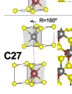
Importantly, other transition metal dichalcoghenides, such as WS2, as well as MoSe2 and WSe2 are expected to have similar properties, Zhu ; Jiang ; Ramasubramaniam ; Feng_PRB2012 and the first experimental demonstrations of monolayer WS2 have just been reported. Terrones2012 All of the above naturally leads us to investigate the electronic properties of transition metal dichalchogenide (TMD) multilayers Castellanos ; Zeng ; Wu12 . Here we report our results on the simplest case, a bilayer of MoS2 and WS2, which both have the same crystal structure and very similar lattice constant. In particular we are interested in how the stacking of different TMD monolayers (see Fig. 1) can result in heterostructures with electronic properties different from the homogeneous TMD monolayers and multilayers,
Our calculations were performed with the Vienna ab-initio package (VASP), VASP1 based on the local density-functional approximation, KS-PR plane-wave basis ( eV) and non-collinear projector-augmented waves (PAW) method. Blochl1 ; Hoobs We treat the both the transition metal orbitals , , together with the Sulphur orbtials and as valence states, and the rest are considered as core. We use the Perdew-Burke-Ernzerhof’s PBE version of generalized gradient approximation to describe the exchange correlation density functional. All calculations are carried out using a 11 supercell with vacuum thickness not smaller than 17 Å. The -centered Monkhorst-Pack’s Monkhorst mesh () of the k-points was used to sample the BZ.
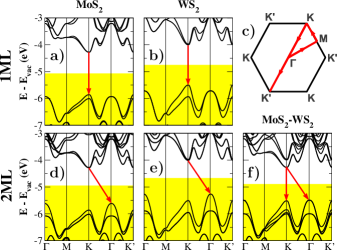
For reference, we discuss first the electronic properties of isolated MoS2 and WS2 monolayers (MLs). Zhu ; Jiang ; Ramasubramaniam ; Feng_PRB2012 ; Cheiw2012 ; Kadantseva The crystal structure of 2H-MoS2 (2H-WS2) consists of two 2D parallel triangular lattices of S atoms separated by the same lattice of Mo (W) atoms translated by of the unit-cell diagonal, with lattice constant Å (Å).Zhu The corresponding Brillouin zone (BZ) is also hexagonal, with two inequivalent and points (valleys). We show the corresponding energy bands in Figs. 2(a) and 2(b)), which are in agreement with previous work using the same methodology.Ramasubramaniam ; Jiang Both MLs are direct band semiconductors with a maximum valence band (VB) and minimum conduction band (CB) located in the and valleys. The band-gap values equal 1.58 and 1.50 eV for MoS2 and WS2 respectively. Our calculations also show that, when referred with respect to the vacuum energy, the band structures of both MLs are shifted (cf. Figs. 2(a) with 2(b)), on account of the different electronegativity of the Mo and W.
Because of the lack of inversion symmetry and a strong spin-orbit coupling (SOC) the valence and conduction bands are spin-split at the and points. The sign of the spin splitting changes from to resulting in the so called strong spin-valley coupling. Xiao The splitting is higher in WS2 ML (435 and 27 meV for VB and CB respectively) than MoS2 ML (147 and 3 meV for VB and CB respectively) due to the higher atomic number of W than Mo.
The band-dependence of the spin splittings is accounted for by the atomic orbital composition of the states. Our population analysis reveals that, at the point, the CB minimum is mostly made by Mo orbitals, whereas the VB maximum dominant contribution comes from the and orbitals. To leading order in the SOC, this should yield a non-zero valley dependent spin-splitting only in the VB, in agreement with the toy model proposed by Xiao et al. Xiao However, both VB and CB states at the points have small contributions coming from the Sulphur and orbitals . These are probably behind the small but finite splitting in the CB.
We now discuss the electronic properties of the bilayers that can be formed stacking the WS2 and MoS2 monolayers. We have verified that the main features of the electronic structure are quite insensitive to the stacking (see Fig. 1 for the different stackings), thereby we focus on the band structure of the C7 stacking (see Fig. 1(b)) presented in Fig. 2(f). This is the stacking of bulk MoS2 and WS2. Comparison of monolayer and bilayer bands in Fig. 2 indicates that interlayer coupling is not strong.
The electronic structure of Mo-Mo and W-W bilayers (Figs. 2(d), (e)) can be rationalized in terms of two concepts: interlayer coupling of degenerate monolayer states, which splits most of the monolayer states, and the existence of a symmetry center in the C7 stacking, which prevents spin splittings. The interlayer splitting is significantly stronger for the valence band at the point than for the VB and CB at K points. As a result, the highest VB state moves to the point for the W-W and Mo-Mo bilayers, which become indirect gap systems.
In the case of the Mo-W heterojunction the interlayer coupling competes with the energy difference of the monolayer states, shown in Fig. 2 (a),(b). As a result, the VB at the point is almost degenerate ( meV) with the top of the VB at the K and K’ points. Consequently, a significant population of photoexcited holes will be available at the K and K’ points, and photoluminescence will be not quenched. In this sense, the MoSWS2 heterojunction – unlike the homogeneous bilayers – will be optically active. In addition, the Mo-W bilayer does not have inversion symmetry, so that spin splittings at the K and K’ points occur like in the monolayers.
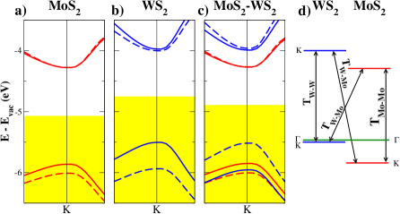
A summary of the electronic states in the neighborhood of the point, relevant for the inter-band optical experiments, both for MoS2, WS2 and the Mo-W bilayer is shown in Fig. 3. It is apparent that interlayer coupling at this point is negligible and the bilayer bands are nothing but a superposition of the monolayer states. As a result, the top of the VB is in the W layer and the bottom of the CB name lies in the Mo layer, forming a type II structure. Cardona-Yu In addition the Mo-W bilayer gap is 1.2eV, 0.3eV smaller than the gap of the monolayers. In contrast, the top of the VB at the point is delocalized in both planes. The resulting scheme of levels is shown in Fig. 3(d). We expect that intra-layer transitions have a stronger quantum yield, on account of their larger electron-hole overlap,Cardona-Yu but relaxation to the lower energy spatially separated electron-hole pair is expected.
We finally comment on the limitations of our methodology. First, PBE is known to underestimate the band gap. The use of either non-local functionals Ramasubramaniam and/or GW approximation Jiang ; Cheiw2012 yields a better agreement with the experiments. Second, excitonic effects, not included in the band structure calculation, are known to produce a large shift in the absorption threshold and photoluminescence peaks. Ramasubramaniam In spite of this, we expect that the band-gap reduction and the segregation of electrons and holes in different atomic planes will be confirmed by experimental work and/or more sophisticated methodologies.
In summary, we have studied the electronic properties of the MoSWS2 system as an example of transition metal dichalcogenide two-dimensional heterostructure. We find that, in contrast to the Mo-Mo and W-W bilayers, the band-gap is direct. Additionally we find that the lowest energy electron and highest energy hole states in the optically active point are localized on different monolayers. In this sense, the Mo-W bilayer forms a type II heterostructure. The combination of band gap engineering in heterojunctions found here, together with the reported electrical control of electronic and optical properties in these systemsRadisavljevic ; Zeng ; Wu12 ; Bolotin , hold the promise of a bright future for optospintronics in two dimensional transition metal dichalcogenides.
We acknowledge J. W. González and F. Delgado for fruitful discussions. This work has been financially supported by MEC-Spain (Grant Nos. FIS2010-21883-C02-01, FIS2009-08744, and CONSOLIDER CSD2007-0010) and Generalitat Valenciana, grant Prometeo 2012-11.
References
- (1) Z. I. Alferov, Review of Modern Physics 73, 767 (2001)
- (2) P. Y. Yu and M. Cardona, Fundamentals of Semiconductors, Springer, New York (1996)
- (3) K. Von Klitzing, Review of Modern Physics 58, 519 (1986)
- (4) D. C. Tsui, H. L. Stormer, and A. C. Gossard, Phys. Rev. Lett. 48, 1559 (1982).
- (5) L. V. Butov, A. L. Ivanov, A. Imamoglu, P. B. Littlewood, A. A. Shashkin, V. T. Dolgopolov, K. L. Campman, and A.C. Gossard, PRL 86, 5608 (2001).
- (6) M. Saba, C. Ciuti, J. Bloch et al.. Nature 214, 731 (2001)
- (7) H. Deng, G. Weihs, C. Santori, C et al., Science 298, 199 (2002)
- (8) M. Kõnig, S. Wiedmann, C. Brune, A. Roth, H. Buhmann, L. W. Molenkamp, X. L. Qi, and S. C. Zhang, Science 318, 766 (2007).
- (9) K. S. Novoselov, D. Jiang, F. Schedin, T. J. Booth, V. V. Khotkevich, S. V. Morozov, and A. K. Geim, Proc. Nat. Ac. Sci. 102, 10451 (2005).
- (10) K. S. Novoselov et al., Nature 438, 197 (2005).
- (11) Y. Zhang et al., Nature 438, 201 (2005).
- (12) K. S. Novoselov and A.H. Castro Neto, Phys. Scr. T146, 014006 (2012).
- (13) K. S. Novoselov, E. McCann, S. V: Morozov, SV; et al. Nature Physics 2 177 (2006)
- (14) C. R. Dean, et al. Nature Nanotech. 5, 722 (2010).
- (15) M. Remskar, A. Mrzel, Z. Skraba, A. Jesih, M. Ceh, J. Demšar, P. Stadelmann, F. Lévy, and D. Mihailovic, Science 292, 479 (2001).
- (16) A. N. Enyashin, L. Yadgarov, L. Houben, I. Popov, M. Weidenbach, R. Tenne, M. Bar-Sadan, and G. Seifert, J. Phys. Chem. C 115, 24586 (2011).
- (17) F.L. Deepak, H.C., S. Cohen, Y. Feldman, R. Popovitz-Biro, D. Azulay, O. Millo, and R. Tenne, J. Am. Chem. Soc. 129, 12549 (2007)
- (18) S. Helveg et al., Phys. Rev. Lett. 84, 951 (2000)
- (19) D. Yang, S. Jiménez-Sandoval, W. M. R. Divigalpitiya, J. C. Irwin, R. F: Drid, Phys. Rev. B.43, 12053 (1991)
- (20) A. Splendiani, L. Sun, Y. Zhang, T. Li, J. Kim, C.-Y. Chim, G. Galli, and F. Wang, Nano Lett. 10, 1271 (2010).
- (21) K. F. Ma, C. Lee, J. Hone. J. Shan, T. F. Heinz, Phys. Rev. Lett. 105, 136805 (2010)
- (22) B. Radisavljevic, A. Radenovic, J. Brivio, V. Giacometti, and A. Kis, Nature Nanotechnology 6, 147 (2011).
- (23) D. Xiao, G.B. Liu, W. Feng, X. Xu, and W. Yao, Phys. Rev. Lett. 108, 196802 (2012).
- (24) T. Cao et al., Nature Communications 3, 887 (2012).
- (25) H. Zeng, J. Dai, W. Yao, D. Xiao, and X. Cui, Nat. Nano. 3, 490 (2012).
- (26) K.F. Mak, K. He,J. Shan, and T.F. Heinz, Nature Nano. 7, 494 (2012).
- (27) G. Sallen, L. Bouet, X. Marie, G. Wang, C. R. Zhu, W. P. Han, Y. Lu, P. H. Tan, T. Amand, B. L. Liu, and B. Urbaszek, Phys. Rev. B 86, 081301(R) (2012).
- (28) Q. Wang, K. Kalantar-Zadeh, A. Kis et al. Nature Nano. 7, 699 (2012)
- (29) Z.Y. Zhu, Y.C. Cheng, and U. Schwingenschlögl, Phys. Rev. B 84, 153402 (2011).
- (30) H. Jiang, J. Phys. Chem. C 116, 7664 (2012).
- (31) A. Ramasubramaniam, Phys. Rev. B 85, 115409 (2012).
- (32) W. Feng, Y. Yao, W. Zhu, J. Zhou, W. Yao, D. Xiao, Phys. Rev. B 86, 165108 (2012)
- (33) H. Gutiérrez et al., arXiv.org 1208.1325 (2012).
- (34) A. Castellanos-Gomez E. Cappelluti, R. Roldan, N. Agrait, F. Guinea, G. Ruibio-Bollinger, Adv. Mater.. doi: 10.1002/adma.201203731
- (35) H. Zeng et al., arXiv 1208.5864 (2012).
- (36) S. Wu et al., arXiv 1208.6069 (2012)
- (37) G. Kresse and J. Furthmüller, Computat. Mater. Sci. 6, 15 (1996). G. Kresse and J. Furthmüller, Phy. Rev. B 54, 11169 (1996).
- (38) W. Kohn and L.J. Sham, Phys. Rev. 140, A1133 (1965).
- (39) P. E. Blöchl, Phys. Rev. B 50, 17953 (1994).
- (40) D. Hobbs, G. Kresse and J. Hafner, Phys. Rev. B 62, 11556 (2000).
- (41) J. P. Perdew, K. Burke, and M. Ernzerhof, Phys. Rev. Lett. 77, 3865 (1996).
- (42) H. J. Monkhorst and J. D. Pack, Phys. Rev. B 13, 5188 (1976).
- (43) T. Cheiwchanchamnagij, W. R. L. Lambrecth Phys. Rev. B 85, 205302 (2012).
- (44) E.S. Kadantseva, and P. Hawrylak, Solid State Commun. 152, 909 (2012).
- (45) A. K. M. Newaz et al, Arxiv 1211.0341