Nonlocal optical generation of spin and charge currents on the surface of magnetic insulators using total absorption and surface plasmons
Abstract
We study the nonlocal spin and charge current generation in a finite metallic element on the surface of magnetic insulators such as yttrium iron garnet due to the absorption of the magnetic surface plasmon (MSP). Whereas a surface plasmon is completely reflected by a metal, an MSP can be absorbed due to the absence of backward states. The injection of MSP generates a voltage in the longitudinal direction parallel to the wave vector, with the voltage proportional to input power. If the metal is a ferromagnet, a spin current can also be induced in the longitudinal direction. Our results provide a way to improve upon integrated circuits of spintronics and spin wave logic devices.
PACS: 78.20.Ls,42.70.Qs,72.15.Gd,73.43.-f
Spintronics, which provides a promising way to overcome the limitation of charged-based electronics in data storage and processing, has received enormous attention recently spintronics . A crucial process in spintronics is the injection of spin and charge currents between structures, at least one of which is magnetic. The injection current is reduced when there is an impedance mismatch across the junction. Improving the injection efficiency is of the utmost importance. The injection can be local as in vertical structures or nonlocal as in planar structures. Nonlocal structures hold the promise for large scale integrated circuits applications. Current nonlocal spin transfer structures nls exploit diffusive spin currents. In this structure, the distance travelled by the signal is equal to the spin diffusion length , and is of the order of 1000 Å. Recently the focus of spin injection in vertical structures has shifted to structures involving magnetic insulators such as yttrium iron garnet (YIG) fmr_yig , where the loss may be smaller.
The exploitation of magnetic surface plasmons (MSPs) in spintronics have not been discussed previously but the MSPs offer many intriguing potentials. MSPs on bulk insulating magnetic surfaces are also known as Damon-Esbach DE magnetostatic modes. They are coupled modes of the surface spin wave and the electromagnetic (EM) wave and are the magnetic analog of the better known (electric) surface plasmons. These states differ from bulk spin waves in that the frequency of these states are in the band gap region and corresponds to nonpropagating bulk spin waves. They differ from surface plasmons in that they are nonreciprocal, because of the broken time reversal symmetry of magnetic systems. This leads to the absence of backscattering, which is also exhibited by electronic ”edge” states in the quantized Hall effect Bert and in topological insulators KM . Stimulated by recent focus on plasmonics, there has been interest in MSPs which can be generated on the surface of magnetic insulators such as YIG yyr .
When an EM wave falls on a metal, it is strongly reflected due to the high impedance mismatch; very little signature of this wave is left in the metal. A surface plasmon has an EM wave component and thus is completely reflected as well when it strikes a metal. In plasmonics, the injection of surface plasmons into metals has never been considered. Whereas a surface plasmon is nearly totally reflected, a MSP incident on a metal is absorbed now that the reflected surface wave is inhibited by the broken time reversal symmetry.
In this Letter, stimulated by a desire to improve upon the spin injection efficiency, to reduce the loss of the signal over distance of nonlocal structures, by recent interests in spin wave logic devices swd and by experimental results of voltage generation in a metal film M on YIG under microwave excitation expt , we study the injection of an MSP into M (which may or may not be ferromagnetic), as is illustrated in Fig. 1. We found that the MSP can be efficiently injected into M by the incoming electric and magnetic field regardless of the interface “impedance mismatch”, generating a static voltage due to the Hall effect in the metal and, also, a spin current if M is a ferromagnet. This provides for the electrical detection of the MSP. In addition, since the transport of the MSP is ballistic, the loss of the signal over propagating distance is much reduced. The distance travelled by the MSP is macroscopic, of the order of a centimeter. It is larger than the spin diffusion length of current nonlocal spin valve structures by five orders of magnitude. Finally, due to the partial spin wave nature of the excitation, the MSP can be easily coupled to spin wave logic devices and provides an efficient connection between different circuit elements. We now describe our results in detail.
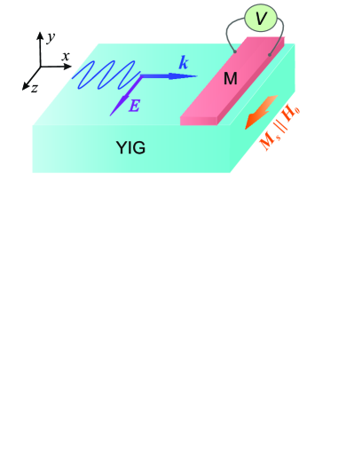
The nonlocal geometry we have in mind is illustrated in Fig. 1. Magnetic surface plasmons can be generated at the surface of a magnetic insulator with an external oscillating RF field, such as from a strip line, away from a finite metallic element M deposited on the surface of a magnetic insulator. In the following we shall illustrate our ideas with parameters such that the magnetic insulator is YIG.
When fully magnetized, a magnetic material is described by a magnetic permeability tensor
| (1) |
where and are of the resonance form: , with a charcteristic bare spin wave frequency . Here is a sum of the external field and the anisotropy field , is the gyromagnetic ratio. measures the coupling strength of the magnetic material with the EM waves and denotes the magnetic damping. For our calculation, we use , , , and the permittivity .
We assume a geometry where the YIG surface and the film is in the plane with the applied magnetic field and the magnetization along the direction. We assume M to have straight edges parallel to the and the axes. The frequency of the MSP at the air-YIG interface as a function of for for the above parameters is illustrated in Fig. 2.
There are four frequencies that are of interest. The bulk spin wave gap at long wavelengths occurs between the spin wave frequency and the frequency . The MSP frequency is in this band gap region where the bulk spin wave states are non-propagating. The other two frequencies are , where the dispersion with negative starts and the frequency , at which the effective magnetic permeability and the dispersion with positive ends. For the above choice of parameters, they are given by GHz, GHz, GHz and GHz. The MSP frequency starts at . In the frequency ranges (yellow region) and (blue region) the frequency of the MSP is defined only for one sign of the wave vector Hart .
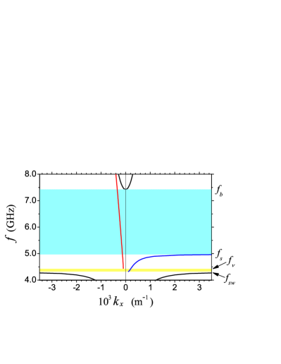
Because of the broken time reversal symmetry of magnetic systems at these frequency ranges there are no MSP states for wave vectors of the other sign. As can be seen from this figure, the group velocities of the two branches of the MSP are of the order of and the speed of light, respectively. The distance travelled is controlled by the damping coefficient and is of the order For the two branches, they range from 10cm to 1000 cm. The extent of the MSP, is of the order of a millimeter.
We next discuss the interaction of the MSP with the metallic film. The usual formulation of spin and charge injection focuses on the matching of the spin and charge current at an interface. In the present case there are no charge current; the boundary occurs in air and there are no discontinuity in the magnetic properties in the YIG substrate. A MSP is a mixture of a spin wave and an EM wave localised near the interface. The MSP is completely described by its EM field, the information of the spin wave is implicitly included in the magnetic susceptibility. The interaction of the MSP and M can thus be formulated in terms of its EM fields.
When an EM field strikes a metal, usually it is strongly reflected. This is what happens with the electric surface plasmon. For the MSP, there are no states with negative s that it can be reflected to. We have considered the possibility that the MSP is stopped at the inteface, then goes along the edges of M and around it. This will involve states with finite and with . We find that states with are not possible. This can be seen from the following physical argument. For a nonzero , the transverse electric (TE) and the transverse magnetic (TM) modes are coupled; the EM wave in YIG have a finite component of the electric field in the direction perpendicular to the film. A finite induces electric charges at the interface and implies that the state will also have an electric surface plasmon character. This is not possible unless one of the dielectric constants is negative.
We have also considered the possibility of the wave going up at the air-M boundary. To this end we have studied states at the air-YIG interface localized near M with imaginary in plane (along x) wave vectors but real wave vectors in the direction perpendicular to the interface (along y). We found that there are no states going up from the air-YIG interface. The only states possible are those coming in from above. Thus there is no surface states for the incoming MSP to escape to and this state can be injected into M. In the following to illustrate our result we consider the case with the MSP wave vector perpendicular to the direction of the magnetization (). The electric field is then along . The tangential electric and magnetic fields and the perpendicular field inside M is the same as that of the incoming MSP as there are no reflected wave. We denote quantities in M and YIG with superscripts M and Y; the quantities in air have no supersctripts. The tangential electric field inside M, , generates a current with current density given by where is the conductivity. Because of the Hall effect, the magnetic field along and this current along z generate an electric field along of magnitude
| (2) |
where ( is the density of the electrons) is the Hall coefficient of M, and the superscript denotes the field due to Hall effect. As we emphasize at the beginning of this paper, the fields only depend on the intrinsic properties of the metal and are not functions of the interface properties and any possible ”impedance mismatch”. The product of and and hence possess finite time independent components. In general M has no electrical leads attached to it and is in an open circuit situation. Charges will be induced at the surface until an electric field of magnitude is developed and the current stops flowing. This corresponds to a voltage where is the length of M in the direction. The total voltage is controlled by the spatial dependence of the EM wave inside M. We show next that the electric field decays in M with a length scale of the order of an effective skin depth.
The electric field in a medium is described by Maxwell’s equation where is the magnetic permeability ; , the dielectric constant. Here we have used units so that the speed of light =1. In principle, the electric field inside M/YIG can be calculated from its value at the boundary with a Green’s function technique gf from the equation
| (3) |
where the surface integral is carried out at the YIG-air YIG-M boundary. is the Green’s function defined by: The operator for for can be constructed from a linear combination of products of photonic states including the M-YIG MSP states as where , are the eigenvalues and the eigenstates of . The Green’s function is dominated by contributions from the MSP states at the air-M-YIG interface with energy when the denominator is zero. Thus the spatial dependence will be determined by these states which we study next. To illustrate the physics we first consider the simpler case where the thickness of M is larger than the spatial extent of the MSP. The MSP state at the air-YIG interface is coupled to the MSP state at the M-YIG interface which can be constructed as follows.
MSP for M/YIG: The properties of the interface MSP state is obtained by matching and of the plane wave states of YIG and that in M. We obtain the dispersion for the YIG-M MSP state given by
| (4) |
Here , , , are the dielectric constant of YIG and M. These states can be excited by the incoming MSP and decays exponentially with a length scale of the order of inverse skin depth away from the air/YIG-M/YIG boundary.
MSP for a trilayer structure: So far we have assumed that the thickness of M is larger than the spatial extent of the MSP. is of the order of a mm. Current experiments are carried out with the thickness of the metallic film of the order of nm and much less than . It is necessary to take the finite thickness of M into account.
We have calculated the interface states in the air/M/YIG trilayer structure by matching the boundary EM fields at both the air/M and the M/YIG interfaces. We found that in the limit when , as given by Eq. (4) is modified so that is replaced by an effective dielectric constant that is reduced by an amount of the order of Furthermore, the real and the imaginary parts of are opposite in sign. In place of Eq. (4) the dispersion is now given by
The two solutions have opposite signs for the real part of The voltage generated is determined by the imaginary part of the wave vector and is given by
| (5) |
where is of the order For and a skin depth of the order of a micron, we obtain We next estimate the magnitude of this effect.
We take M to be Au with a Hall coefficient and a conductivity Thus . We estimate the product from the power of the input coplanar waveguide. We assume that most of the power is expanded in generating the MSP. The energy current
| (6) |
where is the area of the wave. For current experimental systems, the width in the z direction is of the order of a mm; the y extent of the MSP is also of the order of a mm. Thus We obtain Using the above estimate of and for of the order of a watt, is of the order of a micro-volt.
Most metals are paramagnets. Because of YIG, or in the presence of an external magnetic field, the electrons in M has a small magnetization. A nonferromagnetic metal usually do not possess local moments and we do not expect exchange coupling between the YIG spins and this small magnetization in the paramagnet. The electric field generates an AC current inside M. As the electric field oscillates from parallel to opposite the direction of the induced magnetization, a residual DC current can also generated if the resistances along the two directions are different. This can happen if there is a significant amount of spin orbit impurity scattering. The resistance along the two directions will then be different, resulting in a net average current/voltage in this transverse direction. We next consider the situation when the metal is a ferromagnet.
The Hall coefficient of ferromagnets contains a component due to the anomalous Hall effect and the magnitude of the above effect can be modified. In ferromagnets a spin current is also induced. At the air/YIG-M/YIG boundary, the perpendicular component of the magnetic field and the tangential component are continuous. Whereas the magnetization density in air is zero, there is a finite change in the x, y components of the magnetization density at the boundary inside the ferromagnet. We can obtain the magnetization density from the equation . act as sources to create magnetization currents in the ferromagnet. From these we get the magnetization current given by with
| (7) |
| (8) |
Associated with the change in there is a static change in the longitudinal magnetization to second order: . This induces an additional charge current given byfmrprb where is the diffusion constant that relates the charge current to the longitudinal magnetization change. In the open circuit situation, this provides for an additional contribution to the DC potential given by
| (9) |
We next estimate the magnitude of as a function of frequency.
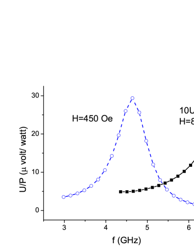
The ratio is of the order of where is the density of states at the Fermi surface; , the Bohr magneton; , the electric charge. From eq. (6) we get We take M to be permalloy with a density of states For the spin wave parameters, we found recentlyChen that the fmr frequency of thin permalloy film as a function of frequency and external field can be fitted by the typical spin wave formula with satutaion magnetization and total field Our estimates for the voltage U normalized by the incoming power P as a function of frequency for the upper branch of the MSP are shown in fig.3 for external fields of magnitudes 850 Oe and 450 Oe. The results for Oe are multiplied by a factor of 10. As can be seen, the magnitude of this contribution is of the order of microvolts. It can exhibit a peak as a function of frequency. This peak is due to the fmr resonance of the permalloy metallic film when is close to zero. The magnitude of this peak depends on the Gilbert damping parameter which we have set to a value of 0.03.
It is likely that the spins of YIG and that of the ferromagnet are exchange coupled. The continuity of and across the YIG-ferromagnet interface imposes partial alignment of the spins between these two materials. Spin currents in the FM will generate some residual spin wave in YIG as well. In the present calculation the exchange coupling between spins can be incorporated in the magnetic susceptibility in eq. (1) by including the exchange energy in .
In conclusion we study the nonlocal spin and charge current generation in a finite metallic element on the surface of magnetic insulators with the magnetic surface plasmon (MSP), which is absorbed and cannot be reflected. The MSP generates a voltage in the longitudinal direction proportional to the power. If the metal is a ferromagnet, a spin current can also be generated in the longitudinal direction. Our result will be useful for new classes of devices using spin waves.
Acknowledgement: John Xiao is supported by DOE under grant number DE-FG02-07ER46374. ZFL is partly supported by the 973 program (2011CB922004).
References
- (1) S. A. Wolf, et al., Science 294, 1486 (2001); I. Zutic, J. Fabian and S. Das Sarma, Rev. Mod. Phys. 76, 323 (2004).
- (2) F. J. Jedema, A. T. Filip, and B. J. van Wees, Nature 410, 345 (2001); T. Kimura, J. Hamrle, Y. Otani, et al., Applied Physics Letters 85, 3501 (2004); Y. Ji, A. Hoffmann, J. E. Pearson, et al., Applied Physics Letters 88, 052509 (2006); Zou Han; Chui S. T.; Wang X. J. and Ji, Y. Physical Review B83, 094402 (2011).
- (3) B. Heinrich, et al., Phys. Rev. Lett. 107, 066604 (2011); Appl. Phys. Lett. 100, 092403 (2012); C.W. Sandweg, Y. Kajiwara, A.V. Chumak, A. A. Serga, V. I. Vasyuchka,1 M. B. Jungfleisch, E. Saitoh, and B. Hillebrands, Phys. Review Lett. 106, 216601 (2011).
- (4) R. W. Damon and J. R. Esbach, Jour. Phys. Chem. Solid, 19, 308 (1960).
- (5) B. I. Halperin, Phys. Rev. B 25, 2185, 2190 (1982).
- (6) C.L. Kane and E.J. Mele, Phys. Rev. Lett. 95 , 226801 (2005).
- (7) S. Y. Liu , Z. F. Lin and S. T. Chui, Appl. Phys. Lett. 97, 2013 (2010); S. T. Chui and Z. F. Lin, J. Phys. Conds. Matt. 22, 182201 (2010).
- (8) For some recent references, see, for example, Y. Kajiwara et al, Nature, 464, 262 (2010). T. Liu and G. Vignale, Phys. Rev. Lett. 106, 247203 (2011).
- (9) Xin Fan, John Q. Xiao, et.al, unpublished (2012).
- (10) A Hartstein, E Burstein, A A Maradudin, R Brewer and R F Wallis, Jour. Phys. C, 6, 1266 (1973).
- (11) S. T. Chui and Z. F. Lin, Jour. Phys. Conds. Matt. 19, 406233, (2007).
- (12) S. T. Chui and Z. F. Lin, Phys. Rev. B. 77, 094432 (2008).
- (13) Yunpeng Chen, Xin Fan, S. T. Chui and J. Q. Xiao, unpublished.