Electronic structure of a subnanometer wide bottom-up fabricated graphene nanoribbon: End states, band gap and dispersion
Abstract
Angle-resolved two-photon photoemission and high-resolution electron energy loss spectroscopy are employed to derive the electronic structure of a sub-nanometer atomically precise quasi-one-dimensional graphene nanoribbon (GNR) on Au(111). We resolved occupied and unoccupied electronic bands including their dispersion and determined the band gap, which possesses an unexpected large value of 5.1 eV. Supported by density functional theory (DFT) calculations for the idealized infinite polymer and finite size oligomers an unoccupied non-dispersive electronic state with an energetic position in the middle of the band gap of the GNR could be identified. This state resides at both ends of the ribbon (end state) and is only found in the finite sized systems, i.e. the oligomers.
pacs:
81.07.Gf, 73.20.-r, 73.20.Hb, 31.15.-pI Introduction
Along with the great interest in graphene that has emerged in recent years Geim2007 , other low-dimensional carbon-based systems attracted attention, one of which are graphene nanoribbons (GNRs). These flat, narrow structures are quasi-one-dimensional and have been subject to numerous theoretical Nakada1996 ; Barone2006 ; Son2006a ; Chaves2011 as well as some experimental studies Han2007 ; Li2008 ; Cai2010 ; Tao2011 since (unlike graphene itself) they exhibit a tunable band gap over a wide range. This is important for their possible implementation in nanoscale devices such as transistors or transparent electrodes whereas they maintain the large carrier mobility found in graphene sheets Geim2007 ; Li2008 . Besides the width, one of the parameters influencing the band gap (and the band dispersion along the ribbon axis) is the edge shape. Depending on the corresponding crystallographic direction in graphene, the ribbon edge’s character varies from armchair to zigzag quasi-continuously Ezawa2006 , much like in carbon nanotubes. The band gap of GNRs are inversely proportional to the ribbon width Barone2006 ; Ezawa2006 yielding gap sizes up to several electron volts in the sub-nanometer regime. Although for a wide range of ribbon widths, this inverse relationship has been experimentally observed Han2007 ; Li2008 and complies with theory, atomically small widths (1 nm) and the corresponding gaps of more than 1 eV have not been observed which is due to the preparation methods employed. Another property of interest is the carrier mobility in GNRs which manifests itself e.g. in the one-dimensional band structure of the ribbons which in first approximation resembles the band structure of graphene projected onto the respective crystallographic direction Nakada1996 . However, the lateral confinement of the electrons in the ribbon alter the dispersion and particularly open a gap at the Dirac point. Theory has dealt in great detail with the dispersion in GNRs whereas there have been no corresponding experiments published so far.
Synthesizing suitable GNRs is challenging, particularly for the established methods such as lithography Han2007 and unzipping carbon nanotubes Kosynkin2009 since in both cases the widths are usually larger than 10 nm and because of defects at the edges influencing the electronic structure. A powerful alternative in the fabrication of nanostructures is the on-surface synthesis Grill2007 , which has been successfully applied for the generation of atomically precise GNRs Cai2010 . Thereby the GNR is formed via a surface- and thermally assisted Bjork2011 two-step process (see Figure 1(a)), in which the adsorbed precursor molecule 10,10’-dibromo-9,9’-bianthryl is dehalogenated followed by C–C coupling to form a polymer and finally cyclodehydrogenation yields the defect-free armchair GNRs with a well-defined width of 0.7 nm.
In this letter, we utilize angle-resolved two-photon photoemission (2PPE) and high resolution electron energy loss spectroscopy (HREELS) to determine the electronic band structure, i.e. unoccupied and occupied electronic states as well as the band gap and dispersion for the GNR shown in Figure 1(a) adsorbed on Au(111). Supported by DFT calculations we demonstrate that the band gap of the ribbon is surprisingly large namely 5.1 eV and contradicts all calculated values known from literature Nakada1996 ; Barone2006 ; Son2006a ; Chaves2011 . An unoccupied electronic state is found in the band gap which possesses no dispersion and originates from the molecular frontier orbitals localized at the ends of the GNR with a finite length.
II Results and Discussion
The thermally activated surface-supported formation steps of the GNR on Au(111) can nicely be followed by angle-resolved vibrational HREELS, since well-defined and pronounced changes in the vibrational spectrum are observed for each step. Fig. 1(b) shows the data for both the polymeric phase and the aromatic nanoribbons.
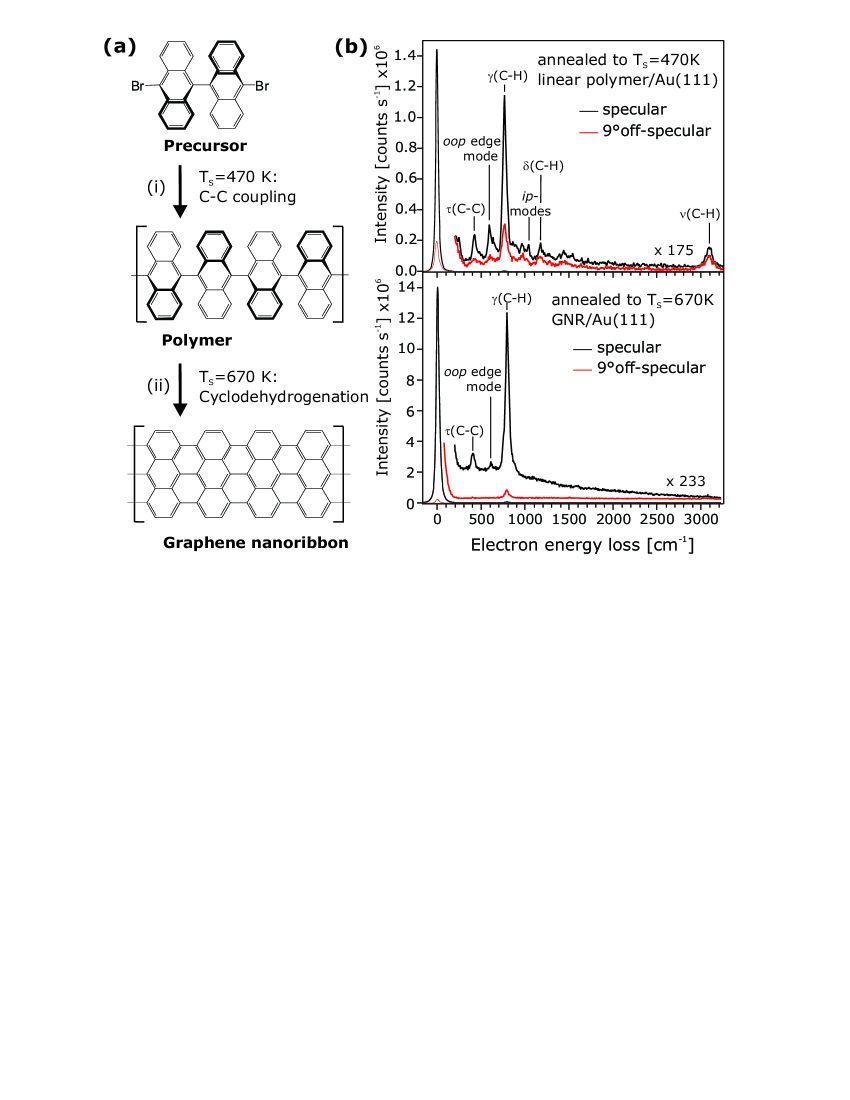
In the specular spectrum of the linear polymer, we observe several out-of-plane molecular vibrations, namely the C–H wagging mode ((C–H)) at 758 cm-1, an edge mode at 594 cm-1 and the phenyl ring torsion modes ((C–C)) at 424 cm-1. All these modes show a drastic decrease in the spectrum measured in off-specular geometry indicating that their intensities are predominantly originating from dipole-scattering, i.e., they are dipole active. Thus, the corresponding dipole moment changes during vibration can be inferred to lie perpendicular to the surface. This points towards a mainly flat adsorption geometry of the phenyl rings in the polymeric phase. Due to the single C–C bonds connecting the building blocks of the polymer and the steric hinderance of the C–H groups, they are slightly tilted as observed in STM Cai2010 . Indeed, at 3055 cm-1 the C–H stretch mode ((C–H)) shows a weak dipole activity. Accordingly this vibration exhibits a component of the dipole moment change parallel to the surface normal which is due to a tilting. Hence, our data fully supports the adsorption geometry reported by Cai et al. Cai2010 . Upon cyclodehydrogenation and thus formation of the nanoribbons, the vibrational spectrum is changed significantly. The number of molecular vibrations found in the spectrum is reduced to three modes. The out-of-plane modes, the phenyl rings torsion mode (C–C) (404 cm-1), the edge mode (609 cm-1) and the bend mode (C-H) at 793 cm-1 are all purely dipole-active. This clearly demonstrates that all phenyl rings are now orientated parallel (flat-lying) to the surface as expected for the aromatic GNR. By adsorption of xenon onto the so prepared GNR-covered surface, we may roughly infer to the coverage of the nanoribbons on the gold surface: in temperature programmed desorption, two desorption peaks are observed which do not grow in intensity, as the layer thickness is increased to very high coverages. These features are assigned to Xe desorbing from both between and on top of the nanoribbons, respectively. From their peak intensities we can roughly infer to a coverage of approximately 2/3 ML.
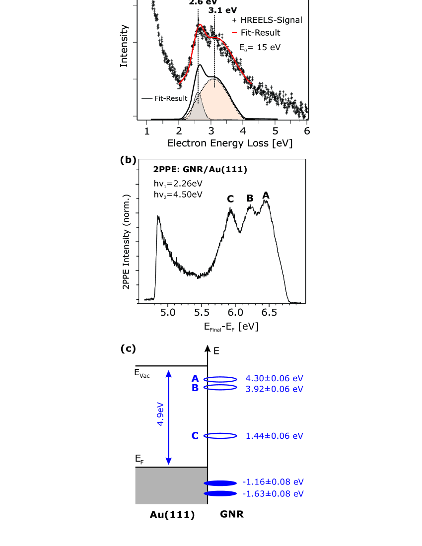
Electronic HREELS as well as 2PPE is employed to gain insights into the occupied and unoccupied GNR-derived electronic states and therefore the band gap. Figure 2(a) shows the result obtained from electronic HREELS using a primary electron energy of =15eV. A double peak structure is observed which we fitted with two Gaussian peaks yielding transition energies of 2.6 eV and 3.1 eV, respectively. An exemplary two-color 2PPE spectrum recorded with 2.26 eV and 4.50 eV photons is displayed in Figure 2(b). Several peaks are observed and on the basis of photon energy dependent measurements Hagen2010 ; Bronner2012 they can be related to photoemission from unoccupied intermediate states. The peaks labeled with A and B are both populated with the 4.50 eV photons and probed by =2.26 eV, thus they are located at 4.30 0.06 eV and 3.92 0.06 eV, respectively, with respect to the Fermi level (). Note that the energetic positions given here are averaged values based on several measurements. The peak labeled C originates from a state which is probed by the 4.50 eV photons, therefore it possesses an energetic position of 1.44 0.06 eV with respect to . Combining the HREELS transition energies with the 2PPE results, we conclude that there are two occupied electronic states lying at -1.16 0.08 eV and -1.63 0.08 eV with respect to . Since these energies do neither comply with the bulk band structure of Au(111) nor with the Shockley surface state, these occupied states can be assigned to the GNR. Figure 2(c) summarizes the the binding energies of all electronic states observed in the present study. On the basis of the obtained data one would establish a band gap of 2.6 eV as found as the lowest transition in the electronic HREELS measurement, which is in reasonable agreement with a recent measurement of the band gap on spatially aligned GNR using ultraviolet and inverse photoemission Linden2012 . However, for an unambiguous identification of the band gap one needs further information on the nature of the unoccupied bands (states). In order to gain deeper insights into the properties we performed dispersion measurements using angle-resolved 2PPE, which provide information about the extent of electron delocalization/localization.
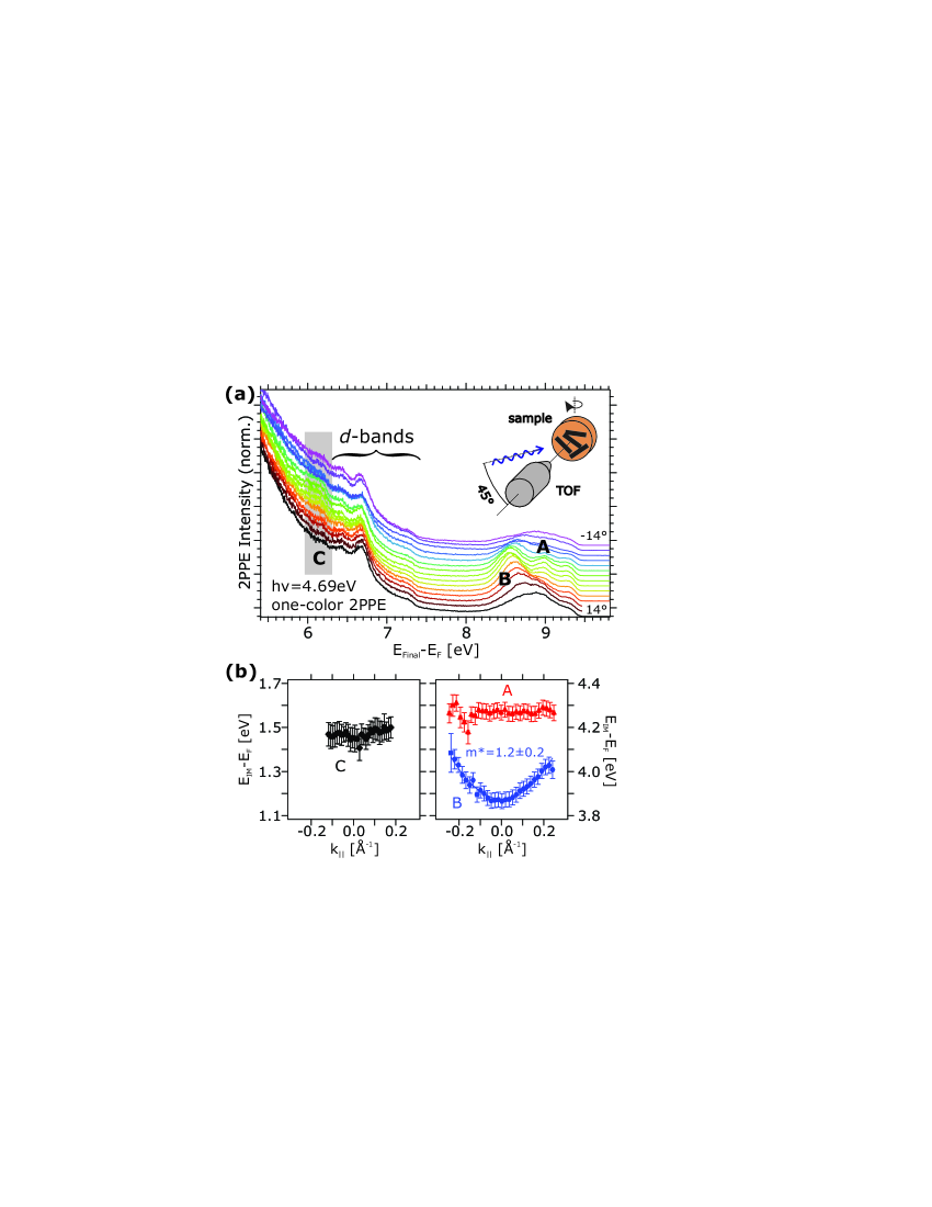
As observed in STM Cai2010 , the GNRs investigated in this study are oriented randomly on the Au(111) surface. In our experiment, the momentum information is obtained by rotating the sample in front of the time-of-flight (TOF) spectrometer as seen in Fig. 3(a). While all nanoribbons contribute to the signal detected in normal emission, this is not the case as we rotate the sample. A photoelectron emitted from the one-dimensional band structure of GNR band has two contributions to its momentum parallel to the surface, i.e. the component along the ribbon axis (which is the quantity of interest) and a component perpendicular to it which is random (as the electrons are localized in this direction). Thanks to the measuring geometry our TOF only detects photoelectrons emitted in the plane perpendicular to the rotation axis. This can either be electrons emitted along the axis of ribbons lying in this plane or electrons which (due to the random momentum perpendicular to the ribbon axis) are emitted at an angle with respect to the ribbon which is equal to the angle between this GNR and the detection plane. In the latter case, the detected momentum will be higher than the momentum the electron had in the band which causes the measured dispersion to be smeared out to higher k but not in energy. Since for finite angles only ribbons lying perpendicular to the rotation axis can be measured, we expect a significant drop in photoemission intensity away from the point.
From the three unoccupied bands observed in 2PPE only the one labeled as B shows a dispersion, viz. the states A and C are localized. Figure 3(a) displays a series of one-color 2PPE spectra recorded at a photon energy of 4.66 eV for various angles between the surface normal and the TOF axis. Beside the contributions of the gold d-bands, the peaks labeled A, B, and C are seen. While B exhibits a strong dispersion around the point, state A and C show no dispersion (see Fig. 3(b)). The parabolic behavior of state B complies qualitatively with all theoretical calculations on armchair nanoribbons. The effective mass () of is significantly higher than theoretical models generally predict for a variety of GNRs Wang2011 ; Yang2007 .
However most surprising the lowest unoccupied state located at 1.44 eV above (peak C) exhibits no dispersion, therefore we assign the first dispersive state (state B) above the Fermi level, which possesses an energetic position of 3.92 eV to the conduction band of the GNR. Thus, with the valence band located at -1.16 eV with respect to the band gap is 5.1 eV. This value is significantly higher than the calculated values lying in the range between 1.5 eV and 2.1 eV depending on the applied method Cai2010 . For the use in technological applications, the size of the band gap plays a key role; the one we observe for the studied armchair GNR is too large for instance the use in a nanowire or even a transistor where a small gap is preferred.
In order to understand the nature of the localized state C we performed DFT calculations for the idealized infinite polymer and finite size oligomers employing the PBE GGA-functional and the range separated hybrid functional CAM-B3LYP, which is particularly suitable for long chain molecular systems (polyene) Yanai2004 together with the 6-311G** basis set as implemented in the Gaussian 09 program package g09 . All calculations were done for the GNR alone, i.e. without the supporting Au(111) surface, and the geometry of the GNR was fully optimized. For the periodic calculations a -point grid with 240 points in the first Brillouin zone (1BZ) and a real space cut off of 600 bohrs were used. The PBE results obtained here compare very well with calculations reported by Cai and coworkers Cai2010 . Furthermore, for the periodic calculations, the geometry of the GNR depends only very weakly on the choice of the functional. For instance, we obtain a lattice constant of 4.310 Å for PBE and for CAM-B3LYP we get 4.277 Å. However, the band gap changes drastically due to the admixture of exact exchange in the CAM-B3LYP functional. Using the PBE functional results in a gap of 1.54 eV, while for CAM-B3LYP a gap of 4.35 eV is obtained. The same qualitative trend is observed when using PBE0 Adamo1999 , i.e., PBE with an admixture of exact exchange, where we obtain a band gab of 2.7 eV. Also, it has been shown, that CAM-B3LYP is especially suitable for structural and electronic properties of large unsaturated hydrocarbons Peach2007 , which is in line with the much better agreement of CAM-B3LYP with the experimental results reported here.
However, apart from the wider band gap and the larger dispersion, the band structures for the PBE and CAM-B3LYP are qualitatively similar and no indication of a non-dispersive state corresponding to the localized state C could be found in the periodic calculations for the idealized infinite polymer.
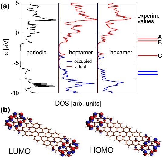
Therefore, we carried out additional calculations for oligomers up to the heptamer, where the oligomers were saturated with hydrogens at both ends and again a full geometry optimization was performed. In order to compare the electronic structure of the oligomers with the one of the periodic structure, we computed the density of states (DOS) by a simple Lorentzian-broadening procedure, where every Kohn-Sham orbital energy or every crystal orbital energy within the 1BZ is represented by a Lorentzian with a width =0.2 eV for the oligomers and =0.1 eV for the periodic case. Figure 4(a) shows the DOS for the periodic case (black line) and for the occupied (blue lines) and virtual, i.e., unoccupied, orbitals (red lines) of the heptamer and the hexamer using the CAM-B3LYP functional. As one can see, the DOS for the valence and the conduction bands are quite similar. The same holds for the geometric structure, as we get a length of 4.278 Å for the monomer unit in the middle of the heptamer, which is nearly identical to the lattice constant of 4.277 Å in the periodic case.
However, for the electronic structure of the oligomers we observe two states inside the “band gap”, namely the highest occupied (HOMO) and lowest unoccupied molecular orbital (LUMO). These states are localized at both ends of the oligomers, as shown in Fig. 4(b) for the heptamer. Furthermore, the energy difference between these two localized states decreases for longer chain lengths. In the experiments GNRs with a length, which corresponds to dozens of units (monomer length: 0.43 nm) Cai2010 , for which a non-resolvable energy difference between the two localized states is to be expected. In addition, the HOMO of the free GNR should also be unoccupied, when adsorbed at the Au(111) surface, as its energy is above the Fermi level. Therefore, these localized states can be identified as state C comparing the calculated energies with experimental determined energies, which are indicated at the right side of Fig. 4(a).
III Conclusion
In conclusion, using two complementary surface-sensitive experimental methods, namely HREELS and 2PPE, in combination with DFT calculations we were able to probe key electronic properties of a defect-free graphene nanoribbon. We determined the band gap to be 5.1 eV, which is surprisingly high since previous calculations predicted much lower values. A non-dispersive unoccupied electronic state of the GNR located in the band gap originates from both the HOMO and LUMO of the ribbons with a finite length (oligomer). These states are localized at both ends of the ribbon, thus we named them ”end states”. A controlled modification of the precursor molecule with suitable substituents or by doping may certainly open the perspective to create precise nanoribbons with lower band gaps, appropriate for applications.
IV Acknowledgement
We gratefully acknowledge financial support by the FU Berlin through the Focus Area ”NanoScale” and by the DFG through the collaborative research center SFB 658. We thank Cornelius Gahl (FU Berlin) for very fruitful discussions.
*petra.tegeder@physik.fu-berlin.de
References
- (1) A. K. Geim and K. S. Novoselov, Nature Materials 6, 183-191 (2007)
- (2) K. Nakada and M. Fujita, Phys. Rev. B 54, 17954-17961 (1996)
- (3) V. Barone, O. Hod, and G. E. Scuseria, Nano Lett. 6(12), 2748-2754 (2006)
- (4) Y.-W. Son, M. L. Cohen, and S. G. Louie, Phys. Rev. Lett. 97, 216803 (2006)
- (5) A. J. Chaves, G. D. Lima, W. de Paula, C. E. Cordeiro, A. Delfino, T. Frederico, and O. Oliveira, Phys. Rev. B 83, 153405 (2011)
- (6) M. Y. Han, B. Özyilmaz, Y. Zhang, and P. Kim, Phys. Rev. Lett. 98, 206805 (2007)
- (7) X. Li, X. Wang, L. Zhang, S. Lee, and H. Dai, Science 319, 1229-1232 (2008)
- (8) J. Cai et al., Nature (London) 466, 470-473 (2010)
- (9) C. Tao et al., Nature Physics 7, 616-620 (2011)
- (10) M. Ezawa, Phys. Rev. B 73, 045432 (2006)
- (11) D. V. Kosynkin, A. L. Higginbotham, A. Sinitskii, J. R. Lomeda, A. Dimiev, B. K. Price, and J. M. Tour, Nature (London) 458, 872-876 (2009)
- (12) L. Grill, M. Dyer, L. Lafferentz, M. Persson, M. V. Peters, and S. Hecht, Nature Nanotechnology 2, 687-691 (2007)
- (13) J. Björk, S. Stafströmm, and F. Hanke, J. Am. Chem. Soc. 133, 14884-14887 (2011)
- (14) S. Hagen, Y. Lou, R. Haag, M. Wolf, P. Tegeder, New. J. Phys. 12, 125022 (2010) 2010, 12, 125022.
- (15) Bronner, C.; Schulze, M.; Hagen, S.; Tegeder P. New J. Phys. 2012, 14, 043032.
- (16) S. Linden, D. Zhong, A. Timmer, N. Aghdassi, J.H. Franke, H. Zhang, X. Feng, K. Müllen, H. Fuchs, L. Chi, H. Zachariasm Phys. Rev. Lett. 108, 216801 (2012).
- (17) G. Wang, Phys. Chem. Chem. Phys., 13, 11939-11945 (2011)
- (18) L. Yang, C.-H. Park, Y.-W. Son, M.L. Cohen, S.G. Louie, Phys. Rev. Lett., 99, 186801 (2007)
- (19) T. Yanai, D. Tew, N. Handy, Chem. Phys. Lett., 51, 393 (2004)
- (20) Gaussian 09, Revision A.02, Frisch, M. J. et al., Gaussian, Inc., Wallingford CT, 2009.
- (21) C. Adamo and V. Barone, J. Chem. Phys., 110, 6158 (1999).
- (22) M.J.G. Peach et al., J. Phys. Chem. A, 111, 11930 (2007).