The transmission spectra of the graphene-based Fibonacci superlattice
Abstract
We consider the gapped graphene superlattice (SL) constructed in accordance with the Fibonacci rule. Quasi-periodic modulation is due to the difference in the values of the energy gap in different SL elements. It is shown that the effective splitting of the allowed bands and thereby forming a series of gaps is realized under the normal incidence of electrons on the SL as well as under oblique incidence. Energy spectra reveal periodical character on the whole energy scale. The splitting of allowed bands is subjected to the inflation Fibonacci rule. The gap associated with the new Dirac point is formed in every Fibonacci generation. The location of this gap is robust against the change in the SL period but at the same time it is sensitive to the ratio of barrier and well widths; also it is weakly dependent on values of the mass term in the Hamiltonian.
pacs:
In recent years both graphene and graphene structures attracted much attention which is naturally explained by their non-trivial propertiesbib1 ; bib2 ; bib3 ; bib4 ; bib5 ; bib6 ; bib7 ; bib8 ; bib9 ; bib10 ; bib11 ; bib12 ; bib13 . On the other hand, notable among the semiconductor structures including graphene ones are superlattices intermediate between periodic and disordered – quasi-periodic structures, e.g. Fibonacci, Thue-Morse and others. This is due to their unusual properties, such as self-similarity, fractal-like electronic spectrum etc. Attempts has already been started to study some kinds of superlattices based on graphene (Fibonacci and Thue-Morse bib10 ; bib11 ) which shed light on the behaviour of Dirac chiral fermions in the quasi-periodic chains. Motivated by these circumstances, in this report we study the energetical spectra of the Fibonacci SL based on the monolayer gapped graphene. Quasi-periodic modulation is due to the difference in the values of the mass term in the Hamiltonian in different elements of the superlattice. Because of the substantial progress in techonology of graphene structures, in particular concerning the fabrication of the gapped graphene bib14 ; bib15 ; bib16 ; bib17 ; bib18 ; bib19 ; bib20 we vary the value of in wide range regardless of its nature which may be different bib14 ; bib15 ; bib16 ; bib17 ; bib18 ; bib19 ; bib20 .
Consider the SL built of two elements “a” and “b”, see Fig. 1.
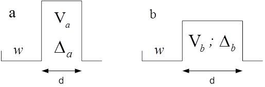
Both elements contain the quantum well of width “w” and a potential barrier of width “d”. The term corresponds to the “a” element and the barrier height is denoted as , for an element “b” we have and respectively. The SL is constructed according to the Fibonacci inflation rule. Thus for the fifth Fibonacci generation one can write : =abaababa. The value of the transmission coefficient , being the electron energy, through the SL built for a certain generation is determined by the period of this generation (sequence). Energy intervals in which the condition holds form the allowed bands in energy spectrum, gaps are associated with values . The transmission coefficient can be evaluated by the transfer matrix method, by expressing either in terms of the Green functions or the eigenfunctions. The latter are the solutions of the Dirac-like equation
| (1) |
where , the momentum operator, , , , — Pauli matrices for the pseudospin, the external potential, which depends only on coordinate , – two-dimensional unit matrix, the mass term is denoted by the symbol as adopted in the literature. The function is a two-component pseudospinor , , are the envelope functions for the graphene sublattices and . Suppose that the potential consists of repetitive rectangular barriers along the -axis and within each -th barrier. Since the -component of the electron momentum commutes with the Hamiltonian one can write and we get from (1):
| (2) |
where , , where units are adopted. If we present solutions for the eigenfunctions as a sum of plane waves traveling in the forward and backward directions of the -axis then we obtain:
| (3) |
where if and otherwise, the top line in (3) pertains to the sublattice , the lower one — to the sublattice . Transfer matrix connecting the wave the functions at the points and is found in several studies (see e.g.bib6 ) and has the form:
| (4) |
where , .
The coefficient of the transmission of quasi-particles through the lattice ,
| (5) |
where is the angle of incidence, and the matrix is expressed as a product of matrices : , — the number of elements in the SL.
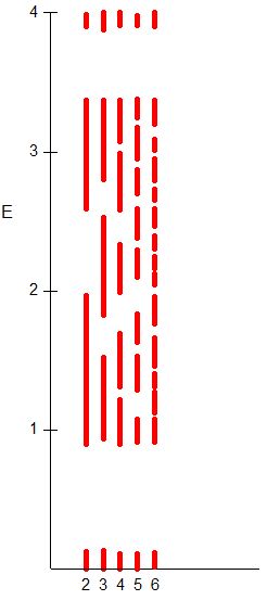
The trace map for 6 initial Fibonacci sequences is depicted in Fig. 2 for the case where we have the gapped graphene in elements “a” and the gapless one in elements “b”. First of all it is noteworthy that the quasi-periodic modulation by setting different values of in different SL elements used in this study results in the efficient splitting of the allowed energy bands and thus in the formation of a number of gaps. And this is realized at normal incidence of the electrons on the lattice.
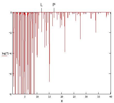
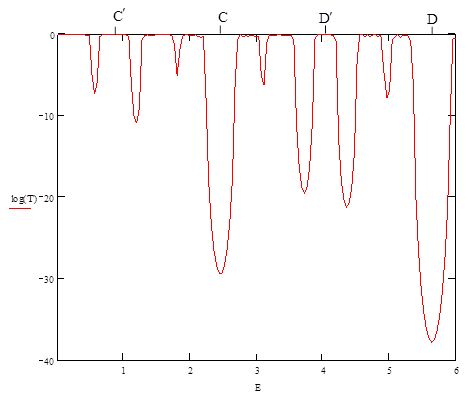
Fig. 3 exhibits the tunneling spectrum, i.e. the dependence of the transmission coefficient T on energy E for the 4-th Fibonacci generation under normal incidence of the electron wave on the lattice; the same spectrum in the energy range is shown in Fig. 4. We see that the structure of some parts of the spectra is repeated periodically throughout the whole energy scale; one of these fragments of the spectrum can be considered as its period. The characteristic features of the period – the number of allowed (forbidden) bands and their widths change so that with E increasing the gap’s widths on average decrease. The natural result of this reduction is that the transmission coefficient asymptotically approaches to unity in the sufficiently far over-barrier region.
The band widths don’t decrease monotonically – with E increasing the alternate extension and reduction of gaps (or the allowed bands) is observed. This results in a wider periods (like a super-period) as it is clearly seen in Fig. 2 (e.g. the interval between the points and ). In other words, the result of such a wavelike changes of band widths is the grouping of smaller structural units into bigger ones to form the additional structural order – a manifestation of the self - similarity in the problem considered.
Spectra similar to that shown in Fig. 3 for the 4-th generation are observed also for other Fibonacci sequences.
The number of bands and the width of each of them depend on one hand on the SL parameters and on the other hand on the number of the generation.
Here we would like to draw attention to a certain contrast to the situation in conventional SL (with a parabolic dispersion law of the charge carriers). Unlike in the conventional SL where the calculation of bands usually is carried out within the barrier region, in graphene Fibonacci structures for this purpose it is advisable to choose the certain energy intervals, e.g. periods of spectra (see Figs. 3, 4) or some other fixed fragments of spectra.
As follows from the calculations, the number of allowed (forbidden) bands contained in one period, in particular in the interval CD in Fig. 4, corresponds to the Fibonacci sequence and this number is subjected to the Fibonacci inflation rule: , where is the number of the Fibonacci generation (see Fig. 2). Note that this rule is applied not only to the CD period but to larger periods as well; every new super-period has its own number of bands.
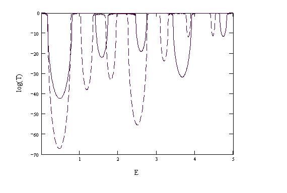
As we can see in Figs. 3, 4 at a certain energy all Fibonacci generations form the gap associated with the new Dirac point – “new Dirac point gap” bib6 . Its location is almost unchanged in different Fibonacci sequences. A typical feature of the new Dirac point gap is that it is independent of the lattice period and at the same time is sensitive to the ratio . This is proved in particular by Fig. 5 which shows the dependence of on for the third Fibonacci generation for different values of and . Once again we draw attention to the fact that the band’s splitting (thereby forming a series of gaps) is realized even in the case of the normal incidence of electrons on the lattice surface. This result is significantly different from what was obtained in bib10 in which a quasi - periodic modulation was created by the difference in the potentials of elements “a” — the barrier and “b” — the well, and the splitting of bands was observed when only (oblique incidence of the wave).
The location of the new Dirac point depends in general on values of each parameter , , , , , and it turns out that if we put , then this position is equal to and only slightly deviates from this value with increasing of is the exact position of the new Dirac point in the periodic lattice bib6 ).
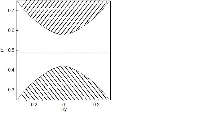
The band structure for the SL of the third Fibonacci generation is shown in Fig. 6 in coordinates , ; it features the spectra dependence on the angle of incidence . Note that there is some extension of the new Dirac gap and at the same time the dependence of other gaps on is very weak (not shown in Fig. 6). This circumstance is known to be common in the study of certain effects in graphene structures, in particular, the same result was stated in bib8 : if there is a sufficiently strong effect at = 0 then the dependence on is weak, see also the comment in bib8 . The dashed line in Fig. 6 denotes the new Dirac point’s location (almost equal to ).
References
- (1) A.K.Geim, K.S.Novoselov, Nat. Materials 6,183 (2007).
- (2) A.N.Castro Neto, F.Guinea, N.M.R.Peres et al., Rev. Mod. Phys. 81,109 (2009).
- (3) J.M.Pereira, F.M.Peeters, A.Chaves et al., Semicond. Science Technology 25,033002 (2010).
- (4) V.V.Cheianov, V.I. Falko, Phys. Rev. B 74, 041403 (2006).
- (5) Q.Zhao, J.Gong, C.A.Muller, Phys. Rev. B 85, 104201 (2012).
- (6) L.Wang, X.Chen, J.Appl. Phys. 109, 033710 (2010).
- (7) L.Wang, S.Zhu, Phys. Rev.B 81, 205444 (2010).
- (8) V.H.Nguyen, A.Bournel, P.Dollfus, Semicond.Sci.Technol. 26,125012 (2011).
- (9) M.Barbier, P.Vasilopoulos, F.M.Peeters, Phys. Rev.B 80,205415 (2009).
- (10) P.Zhao, X.Chen, Appl.Phys. lett. 99, 182108 (2011).
- (11) T.Ma, C.Liang,L.Wang et al., Appl.Phys. lett. 100, 252402 (2012).
- (12) Yu.P.Bliokh, V.Freilikher, S.Savel’ev et al., Phys. Rev. B 79, 075123 (2009).
- (13) P.V.Ratnikov, JETP Letters 90, 469 (2009).
- (14) J.C.Meyer, C.O.Girit, M.F.Crommie et al., Appl. Phys. Lett. 92,123110 (2008).
- (15) P.W.Sutter, J.Flege, E.A.Sutter, Nat. Materials. 7, 406 (2008).
- (16) J.Coraux, A.T.N’Diaye, C.Busse et al., Nano Lett. 8,565 (2008).
- (17) Y.W.Son, M.L.Cohen, S.G.Louie, Phys.Rev.Lett 97,216803 (2006).
- (18) M.Y.Han, B.Ozyilmaz, Y.Zhang et al., Phys. Rev. Lett. 98, 206805 (2007).
- (19) G.Giovanetti, P.A.Khomyakov, G.Brocks et al., Phys. Rev. B 76, 073103 (2007).
- (20) S.Y.Zhou, G.Gweon, A.V.Fedorov et al., Nat. Materials 6,770 (2007).