Unusual temperature dependence of the spectral weight near the Fermi level of NdNiO3 thin films
Abstract
We investigate the behavior of the spectral weight near the Fermi level of NdNiO3 thin films as a function of temperature across the metal-to-insulator transition (MIT) by means of ultraviolet photoelectron spectroscopy. The spectral weight was found to exhibit thermal hysteresis, similar to that of the dc conductivity. A detailed analysis of the temperature dependence reveals two distinct regimes of spectral loss close to the Fermi level. The temperature evolution of one regime is found to be independent from the MIT.
I Introduction
Nickel-based rare-earth perovskite oxides NiO3, with being a trivalent rare earth, are a model system to study temperature-driven metal-to-insulator transition (MIT). They are among the few oxide families that exhibit metallic conductivity and, except for LaNiO3, all nickelates undergo an MIT with a critical temperature that depends on the radius of the rare-earth ion Torrance et al. (1992); Medarde (1997). The MIT in the nickelates is accompanied by a structural transition from an orthorhombic (space group Pbnm) Garcia-Munoz et al. (1992) to a monoclinic structure (space group P21/n) Alonso et al. (1999a); Staub et al. (2002) with a Ni-O bond length disproportionation. The insulating phase is thought to exhibit charge order with two inequivalent Ni sites where the charge from the trivalent ion is split () between two neighboring nickel sites Alonso et al. (1999b, 2000); Staub et al. (2002); Scagnoli et al. (2005); Medarde et al. (2009). For lighter rare earths like Nd and Pr the MIT is accompanied by a magnetic transition from a paramagnetic to an antiferromagnetic ground state with unusual spin order. For heavier rare earths the magnetic transition occurs at lower temperatures than the MIT Garcia-Munoz et al. (1994); Scagnoli et al. (2008).
The origin of the metal-insulator transition is currently under debate. The conduction band of NiO3 is constituted by the covalent bonding of Ni 3d and O 2p orbitals. Initially, nickelates were located in the Zaanen-Sawatzky-Allen scheme Zaanen et al. (1985) at the boundary between charge-transfer insulators and low- metals Torrance and Metzger (1991). Due to their small charge transfer energy , it was argued that nickelates may even be considered as self-doped Mott insulators Mizokawa et al. (2000), where electrons are transferred from the oxygen to the nickel to form a configuration ( denotes a hole in the oxygen ligand). Charge and spin order would then emerge naturally in these compounds Mizokawa et al. (2000); Lee et al. (2011). Alternatively, charge ordering has been suggested to originate from a strong Hunds coupling, which would overcome the Coulomb interaction energy and provide an alternative route to lift the orbital degeneracy in nickelates Mazin et al. (2007). In this picture, nickelates were considered as band insulators rather than Mott insulators. In recent optical experiments, however, it was shown that Mott physics is essential to describe the redistribution of spectral weight Stewart et al. (2011). Finally, recent dynamical mean field theory (DMFT) calculations Wang et al. (2011) suggested that the Ni occupancy is not compatible with an insulating state caused by a Mott transition or charge transfer and that new physics beyond these frameworks might be needed to account for the insulating state in nickelates.
Ultraviolet photoelectron spectroscopy (UPS) is an ideal tool to probe the electronic structure and the effects of electronic correlations. The density of states (DOS) of the valence band is closely related to the measured photoelectron intensity (spectral weight), and changes in the latter can be related to the opening of a gap during the MIT Mizokawa et al. (1991), variation of the bandwidth Kang et al. (1997) or the transfer of spectral weight between different parts of the valence band Monney et al. (2010). Photoemission measurements on NiO3 have been performed on polycrystalline samples Barman et al. (1994); Mizokawa et al. (1995); Medarde et al. (1997); Vobornik et al. (1999); Okazaki et al. (2003) as well as on thin films Eguchi et al. (2009); Galicka et al. (2009); Gray et al. (2011); Bilewska et al. (2010). Measurements on thin films, however, were only conducted using the relatively low resolution x-ray photoemission spectroscopy (XPS). The present work represents the first high resolution UPS measurements on nickelate thin films.
In recent years the synthesis of nickelate thin films has become increasingly popular. Due to the absence of sufficiently large single crystals, epitaxial thin films are the closest system available to study the intrinsic properties of nickelates. In addition, films can be grown sufficiently thin to measure the influence of epitaxial strain on the phase transition Tiwari et al. (2002a); DeNatale and Kobrin (1995); Catalan et al. (2000a); Novojilov et al. (2000); Tiwari et al. (2002b), opening another degree of freedom in the exploration of the phase diagram of nickelates.
In this paper we present an analysis of the temperature dependence of the spectral weight near the Fermi level of NdNiO3 thin films measured with UPS. We compare measurements at different temperatures from well above to well below the phase transition. We study changes in the valence band as well as the loss of spectral weight near the Fermi edge during the transition. The absence of a complete gap opening in the system is investigated by an analysis of the temperature dependent evolution of the spectral weight in the vicinity of the Fermi level. Finally, the loss of spectral weight is separated into two regimes: at and close to the Fermi energy, and reasons for their different-temperature evolutions are discussed.
II Experiment
Epitaxial NdNiO3 thin films were grown on (001)- oriented Nb:SrTiO3 and SrTiO3 substrates by radio-frequency off-axis magnetron sputtering in 0.180 mbar of an oxygen/argon mixture of ratio 1:3 at a substrate temperature of 490°C. More details on the growth conditions and structural characterization of NdNiO3 films can be found in Ref. Scherwitzl et al. (2010). In this study, the film thickness was approximately 100 nm. DC transport measurements were carried out in a four-point configuration between room temperature and 4.2 K in a helium dipping station with a heating/cooling rate of approximately 1 K/min. Four platinum electrodes were deposited in each corner of the sample and the resistance R (or conductance ) was measured in constant current mode. The transition temperature is defined as the temperature where is maximum.
The ex-situ transferred films were cleaned from adsorbates by annealing in an oxygen atmosphere ( mbar) at K for more than two hours. The surface cleanliness was tested using x-ray photoelectron spectroscopy of the C 1s core levels, whereas the quality of the atomic order at the surface could be verified by means of low electron energy diffraction.
The UPS spectra were recorded using an upgraded SCIENTA SES 200 analyzer. S-polarized monochromatic photons from the He Iα line ( eV) of a helium discharge lamp were used to excite the photoelectrons. The base pressure in the chamber did not exceed 410-11 mbar, while the He partial pressure during the measurement was below 510-10 mbar. All spectra were recorded at normal emission with angular integration and with an energy resolution better than 8 meV. The position of the Fermi energy () was determined by fitting the spectral weight of sputtered polycrystalline Nb at a temperature of 17 K. The constant photon flux was verified manually during the measurements and the spectra are not normalized. The results were reproduced on different samples during multiple experiments.
Sample cooling and heating during the photoemission experiments was achieved by thermal contact with LHe and resistive heating of the manipulator at a rate of less than 2 K/min for the high resolution heating ramp and less than 4 K/min during the complete cooling and heating cycle. The samples remained at the lowest temperature for at least one hour before the heating commenced.
III Results & Discussion
The valence band above and below TMIT
In Fig. 1 the valence band of NdNiO3 near is plotted for two temperatures. The spectrum at 20 K (blue) corresponds to the antiferromagnetic insulating phase while the spectrum at room temperature (red) corresponds to the film being in the paramagnetic metallic phase. The inset shows the full valence band plotted for the same two temperatures. It is composed of several features (A-F).
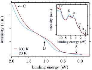
The region has been associated with the band (). It is situated in close proximity to and its character is dominated by the strong hybridization of oxygen and nickel states Sarma et al. (1994); Barman et al. (1994); Mizokawa et al. (1995). Upon cooling the region exhibits a strong loss of spectral weight from the metallic to the insulating phase. Such a behavior is consistent with previous photoemission measurements and has been linked to changes in the initial and final state configuration as well as to an opening of a charge-transfer gap Medarde et al. (1997); Vobornik et al. (1999); Okazaki et al. (2003); Eguchi et al. (2009); Galicka et al. (2009).
The peak ( eV) can be associated with the band of NdNiO3. Ab initio calculations Barman et al. (1994); Sarma et al. (1994) propose a similar strength of orbital hybridization as in the region. At lower temperatures, this feature is shifted by approximately 0.2 eV to higher binding energies. This is compatible with similar changes reported by Eguchi et al. who performed photoemission with a bulk-sensitive excitation energy of eV Eguchi et al. (2009). The nature of this shift might be related to the transfer of spectral weight found in the manganite Pr1/2Sr1/2MnO3 during the MIT Chainani et al. (1997), where a comparable shift of 0.2 eV is present.
The peak ( eV) is expected to be composed of O 2p and, to a smaller part, of Ni 3d states Barman et al. (1994); Sarma et al. (1994). Like the peak, it also shifts by approximately 0.2 eV to higher binding energies. The comparable shifts of both the and the peaks suggest a similar driving force coupling to the binding energy of both features. A precise analysis of the shift of both bands as a function of temperature should provide additional information regarding this hypothesis.
The peak ( eV) and peak ( eV) are considered to be dominated by O 2p states, where, in the case of the peak, localized Nd 4f states also contribute to the spectral weight Sarma and Rao (1980); Barman et al. (1994). At low temperatures both peaks slightly increase in intensity. It seems unlikely that this increase is related to additional adsorption of oxygen at the surface, as x-ray photoemission measurements of the O 1s core level do not show any increased emission at low temperatures. It should be noted that the peak does exhibit a higher intensity compared to what is known from literature. A comparison of different publications shows that this feature is more prominent in thin films Galicka et al. (2009); Eguchi et al. (2009) than in polycrystalline samples Barman et al. (1994); Medarde et al. (1997); Vobornik et al. (1999). This suggests, that the highly coordinated single-crystalline lattice of the thin film samples is a possible reason for this difference.
The peak ( eV) can be identified, by comparison with PrNiO3, to be the result of a photoemission satellite with and character Mizokawa et al. (1995). The suggestion by Galicka et al. Galicka et al. (2009) that a peak at this binding energy might be related to residual carbon at the surface of the sample can be ruled out in the present case due to the absence of C 1s in the XPS measurements. It should be noted that the peak is broadened towards higher binding energies in the insulating phase. Its satellite nature connects this broadening to a change in the electronic configuration of the valence electrons at .
Energy distribution curves at different temperatures
In this paper the focus is set on the strong reduction of spectral weight in the band ( region) crossing . To investigate the intensity loss and its temperature dependence in this region, several high resolution spectra were recorded while the sample was heated from 10 K to ambient temperature.
In Fig. 2 the raw energy distribution curves (EDCs) recorded close to at different temperatures have been plotted. The spectra were obtained during a heating cycle to ensure the fully insulating state of the sample at low temperatures Kumar et al. (2009). A comparison between the highest () and lowest () temperature spectra shows a strong decrease of the spectral weight ( region) between binding energies of approximately 400 meV and . Also visible is a region above 450 meV which exhibits a temperature dependent loss. The latter is, in fact, the tail of the peak shifting to higher binding energies during the MIT (see Fig. 1). In order to highlight the evolution of spectral weight in the region, the EDCs will be separated into two different temperature regimes: a low temperature regime where the sample is in a nominally insulating state, and a temperature regime around the MIT where coexistence of metallic and insulating domains is expected.
The spectra at temperatures up to 80 K do not exhibit any temperature dependence and between 80 K and 130 K only a very weak intensity increase is present. All spectra show a small but finite contribution of spectral weight at and above without a resolvable Fermi edge. Also, an almost linear slope is present in the energy-dependent intensity across the whole region.
The fact that no Fermi edge can be resolved in the low temperature spectra supports the notion of a fully insulating sample without metallic domains. However, there is no complete gap at either, as demonstrated by the residual intensity present even at lowest temperatures. The presence of a gap is expected in the insulating state of a normal MIT. Its absence has to be interpreted as a sign of the unusual nature of the transition.
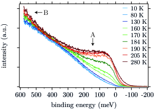
It has been proposed that the abscence of a complete gap in the spectra may be the result of a highly assymetric gap broadended by experimental resolution Vobornik (1999). The valence band onset in such a system would lie very close to but below The measurement process then leads to a convolution between the spectral function including the gap and the instrumental broadening. This, in turn, would result in a residual intensity at in the low temperature spectra.
In Fig. 2 the onset of the resolution-broadened valence band can be estimated to lie between () meV (10 - 80 K) and () meV (130 K) in the insulating regime. The onset at the lowest temperature is compatible with our experimental resolution (8 meV). However, the onset at 130 K ( meV) cannot be explained by resolution broadening, meaning that the system cannot exhibit a complete gap in the insulating phase. This means that the loss of spectral weight has to be caused by a different process. There are several possible explanations for the observed evolution of the spectral weight.
Firstly, the MIT has to be understood as a transition from a metal to a semiconductor with a very low activation energy Granados et al. (1993); Catalan et al. (2000b). In this scenario there is a completely gapped Fermi surface but localized donor or acceptor states are present within the gap. These states, given a high enough density, can contribute to the total photoemission signal with a finite intensity in the photoemission spectra at Higuchi et al. (1998); Aiura et al. (2002). Also, a polaronic in-gap state has been proposed to be present in La1/3Sr2/3FeO3 Wadati et al. (2006) after the system undergoes a transition from a metallic to an insulating state with charge and spin order similar to NdNiO3.
Secondly, in a manner similar to d-wave superconductors Damascelli and Shen (2003) or charge density wave compounds Brouet et al. (2004), only parts of the Fermi surface might actually be gapped, leaving bands crossing to contribute to the spectral weight. The idea of a partially gapped Fermi surface is given support by the fact that optics experiments Katsufuji et al. (1995); Stewart et al. (2011), indicate a gap opening in NdNiO3 while only probing the band structure at the center of the Brillouin zone. In the presence of a Mott type transition this could lead to a zero-size gap Fazekas and Tosatti (1980), where residual density of states remains at temperatures lower than due to an overlap of the upper and lower Hubbard bands at Thouless (1976). Dardel et al. Dardel et al. (1992a) were able to fit residual spectral weight below in the Mott insulator TaS2 using this framework. Similar fits, however, do not converge for the present data.
Another fascinating possibility was presented through calculations of Lee et al. Lee et al. (2011) by an application of DMFT. They argued, that a bond-centered spin-density-wave state could be present in the low temperature phase of the nickelates. This leads to Dirac-cone-like bands crossing with a linear density of states that would resemble the linear spectral weight present in our data. They predict the system to be semi-metallic in the presence of charge order. A gap is only formed if the orthorhombic distortion of the crystal becomes sufficiently high, which might be the case for heavier rare earths. So far, the hypothesis that a gap might emerge in the electronic structure under sufficiently large orthorhombic distortion could not be confirmed by photoemission measurements on EuNiO3 and SmNiO3 Bilewska et al. (2010); Vobornik (1999).
At higher temperatures ( K), a Fermi edge becomes clearly visible in the spectra (Fig. 2) and can be fitted using a polynomial density of states. These fits result in a reasonable effective temperature as well as the correct position of . The emergence of emission from metallic domains is to be expected at temperatures above the critical temperature of the phase transition (see Fig. 3 a). In addition to the emergence of a Fermi edge, the region between the two critical temperatures (see Fig. 3 a) of the MIT ( K) is marked by a sudden increase of the spectral weight that contributes approximately 2/3 of the total loss at . These results are generally in good agreement with previous photoemission experiments on polycrystalline NiO3 crystals. Medarde et al. (1997); Vobornik et al. (1999); Okazaki et al. (2003); Eguchi et al. (2009).
So far, the analysis of the EDCs strongly indicates that no complete gap is present in the electronic structure. It is, however, not clear if the loss of spectral weight in region , as well as the residual intensity at in the low temperature spectra, are the result of a pseudo gap, intensity from a tail of lower-lying O 2p states, donor levels inside the gap, a novel electronic state at low temperatures or a combination of the above. An answer to this question could be obtained by future angle resolved measurements which are able to resolve the dispersion of the electronic bands above and below the MIT.
Comparison of spectral weight and conductivity
Even in the absence of momentum resolved spectra it is still possible to shed further light on the behavior of the electronic states at by comparing the evolution of the effective number of charge carriers with the actual conductivity of the sample. The presence of any kind of gap in the electronic structure is expected to result in a correlation between the transport data and the integrated spectral weight at the Fermi level Dardel et al. (1992b).
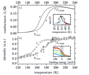
In Fig. 3, the thin film conductance (Fig. 3 a) is compared to the integrated spectral weight at (Fig. 3 b) as a function of temperature in a window around . The top inset shows the temperature derivative of the conductance used to define the critical temperatures of the transition & . The bottom inset illustrates the energy window used to obtain the integrated spectral weight.
The conductance (Fig. 3 a) exhibits a narrow hysteresis ( K) with the MIT temperatures of K on heating and K on cooling (inset in Fig. 3 a). To quantify the extent of the MIT, we define the critical temperatures and for the heating branch. These are estimated as shown in the top inset of Fig. 3 a) to be K and K from the intersection of the blue and red lines respectively. These temperatures mark sharp changes in the conductivity data and thus roughly quantify the boundaries for the phase coexistence region or percolation thresholds for the metallic and insulating states.
The integrated photoemission intensity in Fig. 3 b) is also hysteretic, with critical temperatures that are comparable foo to the values determined from transport. By analogy with the thermal hysteresis in conductivity Catalan et al. (2000b), the observed temperature hysteresis in the spectral weight implies the coexistence of metallic and semiconducting domains during the transition, both contributing individually to the photoemission signal. The determination of by means of an analysis of the integrated spectral weight has been successfully performed on polycrystalline PrNiO3 Medarde et al. (1992). In this work, however, it was possible for the first time to resolve the hysteresis in these systems.
It should be noted that hysteretic behavior has been reported for several other system parameters associated with the MIT. Among these are the temperature dependence of the magnetic moment at the nickel site Medarde (1997); Caytuero et al. (2006); Scagnoli et al. (2006), the unit cell volume Ruello et al. (2005), as well as transport properties like the Seebeck coefficient and the resistivity Granados et al. (1992). The hysteresis in the photoemission data is a demonstration that the MIT is indeed responsible for the loss of spectral weight at .
Temperature-dependent loss of spectral weight
Since the loss of spectral weight at can be connected to the MIT, we will now perform a closer analysis of its temperature and binding energy dependence in the region.
In Fig. 4 the integrated intensity at different binding energies within the region has been plotted as temperature distribution curves (TDCs) obtained during a heating ramp. The intensity was integrated within windows of 25 meV around the annotated binding energies. A variation of this integration window between 3 meV and 100 meV did not lead to a qualitative change of the plot. The curves have been offset against each other for clarity as the room temperature intensities are similar over a broad range of binding energies.
In the vicinity of the strongest feature is the sudden increase of intensity around between the critical temperatures of the MIT and (blue and red dashed lines). This feature completely disappears at higher binding energies where only a linear increase of the spectral weight is present over a broad temperature range (see 300 meV curve).
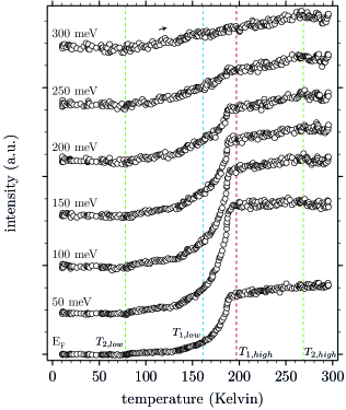
The sudden increase of intensity around the MIT, as well as the absence of a similarly abrupt intensity change in the high binding energy region of the spectral loss, strongly suggest that the overall temperature evolution within the region is actually governed by two regimes ( & ) with distinct temperature dependences.
The fingerprint of the first regime is the sharp rise of intensity during the MIT between 160 and 200 K ( & in Fig. 4). It is most prominent around and its contribution to the total spectral loss vanishes almost completely around binding energies of 250 meV. The correlation between the intensity loss of close to and the MIT was already demonstrated during the comparison of the integrated spectral weight at with the conductivity of the sample (see Fig. 3). Further support is given by the comparison of the temperature dependence of with the effective number of charge carries determined from the integration of the optical conductivity by Katsufuji et al. Katsufuji et al. (1995). They observed a sudden increase in effective carrier density around 150 K and a saturation at 200 K, which is consistent with the temperature dependence of observed in this work, despite the lower temperature resolution of the optical conductivity measurements. It is therefore evident that is directly connected to the physics of the MIT.
The second regime is governed by the linear increase of intensity over a broad temperature range. The intersections of linear fits are at K and K for characteristic temperatures of the linear increase at a binding energy of 300 meV (green dashed lines). These temperatures are, in fact, found to mark a change of the intensity evolution in all TDCs up to . The similarity of the characteristic temperatures in TDCs at all binding energies gives support to the idea that the loss is not only confined to higher binding energies ( meV), but that also governs the temperature evolution at within its respective temperature range together with foo .
A comparison of the characteristic temperatures of ( & ) with those of the MIT (, & ) shows that changes in the TDC that are attributed to are located far away from the MIT and therefore cannot be linked to the phase transition. A connection between and can also be ruled out, as the temperature dependence of the region is similar to that of foo . Another yet unknown process has to govern the temperature evolution of . In this regard it is interesting to note that both temperatures ( & ) are in close proximity to the temperatures reported to be related to changes in the magnetic properties of the system. At a temperature comparable to for instance , Mallik et al. Mallik et al. (1998) found a change in the sign of the magnetoresistance of NdNiO3. At temperatures higher than in the itinerant phase, the evolution of the magnetic moment at the Ni site has been extrapolated to yield a virtual Néel temperature at around 250 K (neutron diffraction) Vobornik (1999); Garcia-Munoz et al. (1994) or 230 K (Mössbauer effect) Caytuero et al. (2006). The latter study also proposed magnons to be present at least in the low temperature regime of the system. The several hundred meV binding energy range of the regime is also compatible with the range of magnon dispersion Delannoy et al. (2009). Also, the presence of a virtual Néel temperature has been suggested Catalan (2008) to be reflected in a change of slope in the susceptibility measured by Zhou et al. Zhou et al. (2000) hinting at a magnetic transition in the itinerant phase.
Although no direct proof of a correlation between magnetic properties and electronic structure in the nickelates can be obtained from our data, the possibility that the observed loss is of magnetic origin certainly merits further study. The correlation between spectral weight and magnetic fluctuations has already been discussed by Kampf et al. for the metallic pseudogap phase of the cuprates Kampf et al. (2000). Future measurements should therefore focus on changes in the electronic structure around these temperatures. Employing techniques other than photoemission, which are sensitive to the magnetic properties of the system, would provide usefull information.
IV Conclusion
By measuring the temperature evolution of the valence band of NdNiO3 thin films, we were able to highlight the subtle changes in the electronic structure of NdNiO3 thin films as a function of temperature. We could further demonstrate the presence of thermal hysteresis in the spectral weight at the Fermi level and relate its evolution to the conductivity of the thin film. The large temperature range investigated together with the high temperature and energy resolution allowed us to distinguish two different loss regimes within the spectral weight close to .
The first regime could be directly related to changes induced by the MIT. Several possible mechanisms responsible for the MIT and the existence of residual intensity at in the insulating phase were discussed. By analyzing the temperature evolution of the spectral weight at various binding energies, a second regime could be identified, which was shown to be completely disconnected from the MIT, with characteristic temperatures for the loss of spectral weight far above and below . After comparison with measurements sensitive to magnetic structure, it was suggested that changes in the magnetic state of the system could be responsible for this interesting temperature behavior.
Acknowledgements.
The authors would like to thank A. J. Millis, D. Baeriswyl, V. K. Malik, C. Battaglia and C. Didiot for helpful discussions as well as the mechanics and electronics workshops in Fribourg and Geneva for their support. This project was supported by the Fonds National Suisse pour la Recherche Scientifique through Division II and the Swiss National Center of Competence in Research MaNEP.References
- Torrance et al. (1992) J. B. Torrance, P. Lacorre, A. I. Nazzal, E. J. Ansaldo, and C. Niedermayer, Physical Review B 45, 8209 (1992).
- Medarde (1997) M. Medarde, Journal of Physics: Condensed Matter 9, 1679 (1997).
- Garcia-Munoz et al. (1992) J. L. Garcia-Munoz, J. Rodriguez-Carvajal, P. Lacorre, and J. B. Torrance, Physical Review B 46, 4414 (1992).
- Alonso et al. (1999a) J. A. Alonso, M. J. Martinez-Lope, M. T. Casais, M. G. A. Aranda, and M. Fernandez-Diaz, Journal of the American Chemical Society 121, 4754 (1999a).
- Staub et al. (2002) U. Staub, G. I. Meijer, F. Fauth, R. Allenspach, J. G. Bednorz, J. Karpinski, S. M. Kazakov, L. Paolasini, and F. d’Acapito, Physical Review Letters 88, 126402 (2002).
- Alonso et al. (1999b) J. A. Alonso, J. L. Garcia-Munoz, M. T. Fernandez-Diaz, M. A. G. Aranda, M. J. Martinez-Lope, and M. T. Casais, Physical Review Letters 82, 3871 (1999b).
- Alonso et al. (2000) J. A. Alonso, M. J. Martinez-Lope, M. T. Casais, J. L. Garcia-Munoz, and M. T. Fernandez-Diaz, Physical Review B 61, 1756 (2000).
- Scagnoli et al. (2005) V. Scagnoli, U. Staub, M. Janousch, A. Mulders, M. Shi, G. I. Meijer, S. Rosenkranz, S. Wilkins, L. Paolasini, J. Karpinski, et al., Physical Review B 72, 155111 (2005).
- Medarde et al. (2009) M. Medarde, C. Dallera, M. Grioni, B. Delley, F. Vernay, J. Mesot, M. Sikora, J. A. Alonso, and M. J. Martinez-Lope, Physical Review B 80, 245105 (2009).
- Garcia-Munoz et al. (1994) J. L. Garcia-Munoz, J. Rodriguez-Carvajal, and P. Lacorre, Physical Review B 50, 978 (1994).
- Scagnoli et al. (2008) V. Scagnoli, U. Staub, Y. Bodenthin, M. Garcia-Fernandez, A. M. Mulders, G. I. Meijer, and G. Hammerl, Physical Review B 77, 115138 (2008).
- Zaanen et al. (1985) J. Zaanen, G. A. Sawatzky, and J. W. Allen, Physical Review Letters 55, 418 (1985).
- Torrance and Metzger (1991) J.B. Torrance and R. M. Metzger, Physica C: Superconductivity 182, 351 (1991).
- Mizokawa et al. (2000) T. Mizokawa, D. I. Khomskii, and G. A. Sawatzky, Physical Review B 61, 11263 (2000).
- Lee et al. (2011) S. B. Lee, R. Chen, and L. Balents, Physical Review B 84, 165119 (2011).
- Mazin et al. (2007) I. I. Mazin, D. I. Khomskii, R. Lengsdorf, J. A. Alonso, W. G. Marshall, R. M. Ibberson, A. Podlesnyak, M. J. Martinez-Lope, and M. M. Abd-Elmeguid, Physical Review Letters 98, 176406 (2007).
- Stewart et al. (2011) M. K. Stewart, J. Liu, M. Kareev, J. Chakhalian, and D. N. Basov, Physical Review Letters 107, 176401 (2011).
- Wang et al. (2011) H. Park, A. J. Millis, and C. A. Marianetti, Physical Review Letters 109, 156402 (2012).
- Mizokawa et al. (1991) T. Mizokawa, H. Namatame, A. Fujimori, K. Akeyama, H. Kondoh, H. Kuroda, and N. Kosugi, Physical Review Letters 67, 1638 (1991).
- Kang et al. (1997) J. S. Kang, D. W. Hwang, C. G. Olson, S. J. Youn, K. C. Kang, and B. I. Min, Physical Review B 56, 10605 (1997).
- Monney et al. (2010) C. Monney, E. F. Schwier, M. G. Garnier, N. Mariotti, C. Didiot, H. Cercellier, J. Marcus, H. Berger, A. Titov, H. Beck, et al., New Journal Of Physics 12, 125019 (2010).
- Barman et al. (1994) S. R. Barman, A. Chainani, and D. D. Sarma, Physical Review B 49, 8475 (1994).
- Mizokawa et al. (1995) T. Mizokawa, A. Fujimori, T. Arima, Y. Tokura, N. Mōri, and J. Akimitsu, Physical Review B 52, 13865 (1995).
- Medarde et al. (1997) M. Medarde, D. Purdie, M. Grioni, M. Hengsberger, Y. Baer, and P. Lacorre, EPL (Europhysics Letters) 37, 483 (1997).
- Vobornik et al. (1999) I. Vobornik, L. Perfetti, M. Zacchigna, M. Grioni, G. Margaritondo, J. Mesot, M. Medarde, and P. Lacorre, Physical Review B 60, 8426 (1999).
- Okazaki et al. (2003) K. Okazaki, T. Mizokawa, A. Fujimori, E. V. Sampathkumaran, M. J. Martinez-Lope, and J. A. Alonso, Physical Review B 67, 073101 (2003).
- Eguchi et al. (2009) R. Eguchi, Y. Okamoto, Z. Hiroi, S. Shin, A. Chainani, Y. Tanaka, M. Matsunami, Y. Takata, Y. Nishino, K. Tamasaku, et al., Journal of Applied Physics 105, 056103 (2009).
- Galicka et al. (2009) K. Galicka, J. Szade, P. Ruello, P. Laffez, and A. Ratuszna, Applied Surface Science 255, 4355 (2009).
- Gray et al. (2011) A. X. Gray, A. Janotti, J. Son, J. M. Lebeau, S. Ueda, Y. Yamashita, K. Kobayashi, A. M. Kaiser, R. Sutarto, H. Wadati, et al., Physical Review B 84, 075104 (2011).
- Bilewska et al. (2010) K. Bilewska, E. Wolna, M. Edely, P. Ruello, and J. Szade, Physical Review B 82, 165105 (2010).
- Tiwari et al. (2002a) A. Tiwari, C. Jin, and J. Narayan, Applied Physics Letters 80, 4039 (2002a).
- DeNatale and Kobrin (1995) J. DeNatale and P. Kobrin, Journal of Materials Research 10, 2992 (1995).
- Catalan et al. (2000a) G. Catalan, R. M. Bowman, and J. M. Gregg, Journal of Applied Physics 87, 606 (2000a).
- Novojilov et al. (2000) M. A. Novojilov, O. Y. Gorbenko, I. E. Graboy, A. R. Kaul, H. W. Zandbergen, N. A. Babushkina, and L. M. Belova, Applied Physics Letters 76, 2041 (2000).
- Tiwari et al. (2002b) A. Tiwari, C. Jin, and J. Narayan, Appl. Phys. Lett. 80, 4039 (2002b).
- Scherwitzl et al. (2010) R. Scherwitzl, P. Zubko, I. G. Lezama, S. Ono, A. F. Morpurgo, G. Catalan, and J.-M. Triscone, Advanced Materials 22, 5517 (2010).
- Sarma et al. (1994) D. Sarma, N. Shanthi, and P. Mahadevan, Journal of Physics: Condensed Matter 6, 10467 (1994).
- Chainani et al. (1997) A. Chainani, H. Kumigashira, T. Takahashi, Y. Tomioka, H. Kuwahara, and Y. Tokura, Physical Review B 56, R15513 (1997).
- Sarma and Rao (1980) D. Sarma and C. Rao, Journal of Electron Spectroscopy and Related Phenomena 20, 25 (1980).
- Kumar et al. (2009) D. Kumar, K. P. Rajeev, J. A. Alonso, and M. J. Martinez-Lope, Journal of Physics: Condensed Matter 21, 185402 (2009).
- Vobornik (1999) I. Vobornik, PhD Thesis - École Polythechnique Fédérale de Lausanne (Switzerland) (1999).
- Granados et al. (1993) X. Granados, J. Fontcuberta, X. Obradors, L. Manosa, and J.B. Torrance, Physical Review B 48, 11666 (1993).
- Catalan et al. (2000b) G. Catalan, R. M. Bowman, and J. M. Gregg, Physical Review B 62, 7892 (2000b).
- Higuchi et al. (1998) T. Higuchi, T. Tsukamoto, N. Sata, M. Ishigame, Y. Tezuka, and S. Shin, Physical Review B 57, 6978 (1998).
- Aiura et al. (2002) Y. Aiura, I. Hase, H. Bando, T. Yasue, T. Saitoh, and D. Dessau, Surface Science 515, 61 (2002).
- Wadati et al. (2006) H. Wadati, A. Chikamatsu, M. Takizawa, R. Hashimoto, H. Kumigashira, T. Yoshida, T. Mizokawa, A. Fujimori, M. Oshima, M. Lippmaa, M. Kawasaki,and H. Koinuma, Physical Review B 74, 115114 (2006).
- Damascelli and Shen (2003) A. Damascelli and Z.-X. Shen, Reviews of Modern Physics 75, 473 (2003).
- Brouet et al. (2004) V. Brouet, W. L. Yang, X. J. Zhou, Z. Hussain, N. Ru, K. Y. Shin, I. R. Fisher, and Z. X. Shen, Physical Review Letters 93, 126405 (2004).
- Katsufuji et al. (1995) T. Katsufuji, Y. Okimoto, T. Arima, Y. Tokura, and J.B. Torrance, Physical Review B 51, 4830 (1995).
- Fazekas and Tosatti (1980) P. Fazekas and E. Tosatti, Physica B+C 99, 183 (1980).
- Thouless (1976) D. J. Thouless, Le Journal de Physique Colloques 37, C4 (1976).
- Dardel et al. (1992a) B. Dardel, M. Grioni, D. Malterre, P. Weibel, Y. Baer, and F. Lévy, Physical Review B 45, 1462 (1992a).
- Dardel et al. (1992b) B. Dardel, M. Grioni, D. Malterre, P. Weibel, Y. Baer, and F. Lévy, Physical Review B 46, 7407 (1992b).
- (54) Note the measured temperatures used for the photoemission data are offset from the actual sample temperatures due to the difference in heat conductance between LHe-thermocouple and LHe-sample, respectively.
- Medarde et al. (1992) M. Medarde, A. Fontaine, J. L. Garcia-Munoz, J. Rodriguez-Carvajal, M. DeSantis, M. Sacchi, G. Rossi, and P. Lacorre, Physical Review B 46, 14975 (1992).
- Caytuero et al. (2006) A. Caytuero, H. Micklitz, F. J. Litterst, E. M. Baggio-Saitovitch, M. M. Abd-Elmeguid, and J. A. Alonso, Physical Review B 74, 094433 (2006).
- Scagnoli et al. (2006) V. Scagnoli, U. Staub, A. M. Mulders, M. Janousch, G. I. Meijer, G. Hammerl, J. M. Tonnerre, and N. Stojic, Physical Review B 73, 100409 (2006).
- Ruello et al. (2005) P. Ruello, B. Perrin, T. Pezeril, V. Gusev, S. Gougeon, N. Chigarev, P. Laffez, P. Picart, D. Mounier, and J. Breteau, Physica B: Condensed Matter 363, 43 (2005).
- Granados et al. (1992) X. Granados, J. Fontcuberta, X. Obradors, and J. B. Torrance, Physical Review B 46, 15683 (1992).
- (60) A change of intensity due to de- and adsorbtion of residual gas layers during the temperature ramp can be ruled out as temperature dependent desorbtion processes are typically confined to much smaller time and temperature scales due to the activated nature of the desorption.
- (61) Unpublished work.
- Mallik et al. (1998) R. Mallik, E. Sampathkumaran, J. A. Alonso, and M. Martinez-Lope, Journal of Physics: Condensed Matter 10, 3969 (1998).
- Delannoy et al. (2009) J. Y. P. Delannoy, M. J. P. Gingras, P. C. W. Holdsworth, and A. M. S. Tremblay, Physical Review B 79, 235130 (2009).
- Catalan (2008) G. Catalan, Phase Transitions 81, 729 (2008).
- Zhou et al. (2000) J. S. Zhou, J. B. Goodenough, B. Dabrowski, P. W. Klamut, and Z. Bukowski, Physical Review Letters 84, 526 (2000).
- Kampf et al. (2000) A. P. Kampf, and J. R. Schrieffer Physical Review B 42, 7967 (1990).