Conductance enhancement due to atomic potential fluctuations in graphene
Abstract
We solve the Dirac equation, which describes charge massless chiral relativistic carriers in a two-dimensional graphene. We have identified and analysed a novel pseudospin-dependent scattering effect. We compute the tunneling conductance and generalize the analytical result in the presence of the tunable atomic potential of a graphene strip. The absence of back scattering in graphene is shown to be due to Berry’s phase which corresponds to a sign change of the wave function under a spin rotation of a particle. We use the transfer matrix approach and find that the electric conductance of doped graphene increases due to atomic potential fluctuations.
pacs:
73.22.Pr, 72.80.Tm, 72.10.FkI Introduction
Graphene is a single layer of carbon atoms densely packed in a honeycomb lattice. This material was found in its free state only recently, when individual graphene samples of a few microns in size were isolated by micromechanical cleavage of graphite Novoselov-1 . The current intense interest in graphene is driven by both the unusual physics involved and a realistic promise of device applications. Among relativistic like phenomena observed in graphene so far, there are two new types of the integer quantum Hall effect and the presence of minimal metallic conductivity of about one conductivity quantumSlon-1 . Transport properties of graphene are interesting because of their unique topological structure Voz-1 ; Bolmat-1 ; bolmat-2 ; Roy-1 . There have been some reports on experimental study of transport in graphene Geim-1 . Various calculations have been performed to understand energy bands of graphene Shyt-1 ; Loz-1 . It has been successful in the study of various properties including the Aharonov-Bohm effect Morp-1 , optical absorption spectra MKatsnelson-1 , quantum tunneling in graphene-based structures bolmat-3 ; zavialov-1 ; bolmat-4 , ferromagnetism ming-1 and instabilities in the presence and absence of a magnetic field Loz-2 .
In a two-dimensional world, there are two basic motions: forward and backward. Random scattering can cause them to mix, which leads to resistance. Just as we have learned from the basic traffic control, it would be much better if we could spatially filter the counterflow directions. This effect could be used to produce a valley-polarized current out of an unpolarized stream of electrons due to line defect particularly in graphene Gunlycke-1 ; feng-1 ; Gun-2 ; golub-1 ; ram-1 ; liw-1 ; feng-2 ; chi-1 ; Leo-1 ; hy-1 .
The electronic transport properties of graphene with defects and impurities exhibit pronounced differences from those of conventional two dimensional electron systems investigated in the past. The basic question that we seek to answer is what happens to the tunneling as we approach the Dirac point of zero carrier concentration with the presence of electrically charged scatters.
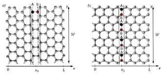
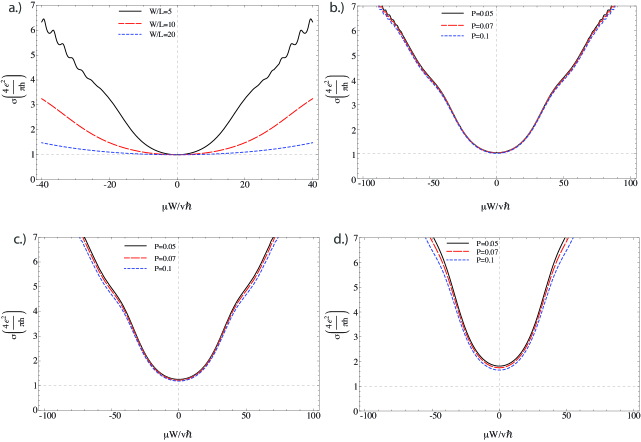
In the present work we consider the effects of atomic potential fluctions in the setup depicted in fig. 1. At low doping the conductance is determined by quasiparticle tunneling, which is independent of the boundary conditions in the -direction if .
II back scattering in graphene
II.1 General consideration
The quasiparticle excitation spectrum of the graphene-based junction consists of the positive eigenvalues of the Dirac equation. The Dirac equation has the form of two equations for electron and hole wavefunctions . In this study we restrict ourselves to the single-valley Dirac equation for graphene
| (1) |
where is a spinor of wave amplitudes for two nonequivalent sites of the honeycomb lattice. The Fermi energy and the impurity potential V (x, y) in the graphene sample () are considered to be much smaller than the Fermi energy in the ideal metallic leads ( and ). For zero doping the conductance is determined by the states at the Dirac point, . Transport properties at finite energies determine the conductance of doped graphene.
Since for aspect ratios the boundary conditions in the -direction are irrelevant, so we take periodic boundary conditions for simplicity. Different wave vectors =2n/W (with n=0, 1, 2, …) in the -direction parallel to the interfaces(at the points and ) and not coupled, so we can consider each transverse mode separately. Without impurity in the bulk at a given energy and transverse wave vector we have up to two basis states
| (5) |
with the definitions
| (6) | |||
| (7) |
The angle (-/2,/2) is the angle between the initial and final wave vectors and . With this sign convention the state move in the , while move in the direction. The factor ensure that two states carry the same particle current.
Considering a back scattering process in an arbitrary external potential we will confine ourselves to states in the vicinity of the point, but the extension to states near a point is straightforward. We have and . Rotation in spin space can be obtained through the replacement corresponding to the electron motion of a time-reversal path. When the wave vector is rotated in the anticlockwise direction adiabatically as a function of time around the origin for a time interval , the wavefunction is changed into , where is the ”spin” part of an eigenfunction of the Eq. 1 and is Berry’s phase. Choosing in such a way that the wave function becomes continuous as a function of and given by
| (8) |
This shows that the rotation in the space by leads to the change in the phase by , i.e., a sign change. A similar phase change of back scattering process is the origin of the so-called anti-localization effect in systems with strong spin-orbit scatteringLarkin-1 . This anti-localization effect was observed experimentally Kom-1 ; Ber-1 . The absence of back scattering can be destroyed by various effects. When the potential range becomes shorter than the lattice constant, the back scattering appears two reasons. The first is the appearance of inter-valley matrix elements between and points And-1 . The second, which we investigate in this work, is that the effective potential of an impurity for and sites in honeycomb lattice can be different. This causes mixing of the spin space and the momentum space.
II.2 Long range impurities
There is an absence of back scattering for long range impurities. This can be seen easily: using the formalism of the previous subsection we can simply show that the matrix element of the back-scattering process is zero
| (15) |
(here is the unit cell area of the graphene lattice). This is rather dramatic since all real materials have impurities, and it is normally these which determine the transport properties of the material. However, in the case of graphene the impurities don’t scatter, i.e. they are effectively not there, and hence one has the possibility of coherent transport in graphene.
III transfer matrix approach
We first determine the transfer matrix of the th mode through the undoped graphene ribbon. The evolution of inside the graphene sample can be written as , where the transfer matrix should satisfy a generalized unitarity condition
| (16) |
In general Eq.II.2 (ignoring an irrelevant scalar phase factor) restricts to a three-parameter form
| (17) |
The real parameters , , depend on the boundary at the scale of the lattice constant and they cannot be determined from the Dirac equations. In this work we consider the ideal interfaces and case, when . From the Dirac Eq.1 we obtain the differential equation
| (18) |
with solution for
| (19) |
where is the longitudinal wave vector, is the transversal wave vector. The total transfer matrix through the impurity-free graphene ribbon () is
| (20) |
Now we construct the transfer matrix for the electron (hole) quasiparticle excitations in the graphene ribbon for disorder potential case, where is the charged impurity potential given by a diagonal matrix, i.e.,
| (24) |
where () is the corresponding microscopic potential and smooth on atomic scales, which is localized along a line and placed in the zone corner () of sublattice (). The Fermi-energy and impurity potential (Eq.24) in graphene sample () are considered to be much smaller than the Fermi-energy in the ideal metallic leads ( and ). For zero doping the conductance is determined by the states at the Dirac point, . Transport properties at finite energies determine the conductance of doped graphene.
The great physical and analytical advantage of the matrix is that it is . In order to obtain transfer matrix for disorder region (along line ) graphene we integrate Eq. 1
Making use of well-known algebraic property for Pauli matrices
| (28) |
we easily obtain the final form for total transfer matrix in disorder graphene sample
| (29) |
where
| (33) |
and . The transfer matrix of the whole sample is straightforwardly related to the matrices of transmission and reflection amplitudes
| (37) |
The conductance of the graphene strip is expressed through the transmission amplitudes by the Landauer formula
| (38) |
where . At the Dirac point the transmission probability for the case reads
| (39) |
When parameters and the Eq.39 reduces to equation , derived in the paper Ben-1 . Parameter reperesents atomic potential fluctuations, when finite .
IV Conclusion
In this paper we used the transfer matrix approach to calculate the tunneling conductance. We generalize the analytical result in the presence of the tunable atomic potential of a graphene strip and find that the electric conductance of doped graphene increases due to atomic potential fluctuations. The absence of back scattering in graphene is shown to be due to Berry’s phase which corresponds to a sign change of the wave function under a spin rotation of a particle. We have identified and analysed a novel pseudospin-dependent scattering effect. The low cost experimental techniques allow for easy verification of the proposed hypothesis.
V Acknowledgements
We are indebted to Ben Still for assistance. D. B. thanks Myerscough Bequest for financial support. D. B. acknowledges Thomas Young Centre for Junior Research Fellowship and Cornell University (Neil Ashcroft and Roald Hoffmann) for hospitality.
References
- (1) K. S. Novoselov, A. K. Geim, S. V. Morozov, D. Jiang, M. I. Katsnelson, I. V. Grigorieva, S. V. Dubonos, and A. A. Firsov, Nature 438, 197 (2005).
- (2) J. C. Slonczewski and P. R. Weiss, Phys. Rev. 109, 272 (1958); G. W. Semenoff, Phys. Rev. Lett. 53, 2449 (1984); F. D. M. Haldane, Phys. Rev. Lett. 61, 2015 (1988); J. Gonzalez, F. Guinea, and M. A. H. Vozmediano, Nucl. Phys. B406, 771 (1993);
- (3) Fernando de Juan, A. Cortijo, and Mara A. H. Vozmediano, Phys. Rev. B 76, 165409 (2007).
- (4) D. Bolmatov and C.-Y. Mou, Physica B: Condensed Matter 405, 2896 (2010).
- (5) D. Bolmatov, C.-Y. Mou, JETP 110, 612 (2010).
- (6) J. K. Pachos, M. Stone, and K. Temme, Phys. Rev. Lett. 100, 156806 (2008).
- (7) C. Casiraghi, A. Hartschuh, E. Lidorikis, H. Qian, H. Harutyunyan, T. Gokus, K. S. Novoselov, and A. C. Ferrari, Nano Lett. 7 (9), 2711 (2007).
- (8) A. Shytov, M. Rudnerb, Nan Guc, M. Katsnelson and L. Levitov, Solid State Commun. 149, 1087 (2009).
- (9) Yu. E. Lozovik and A. A. Sokolik, Phys. Lett. A 374, 326 (2009).
- (10) S. Russo, Jeroen B. Oostinga, D. Wehenkel, H. B. Heersche, S. S. Sobhani, L. M. K. Vandersypen, and A. F. Morpurgo, Phys. Rev. B 77, 085413 (2008).
- (11) M. I. Katsnelson, EPL 84, 37001 (2008).
- (12) D. Bolmatov and C.-Y. Mou, JETP 112, 102 (2011).
- (13) D. V. Zavialov, V. I. Konchenkov and S. V. Kruchkov, Semiconductors 46, 109 (2012).
- (14) D. Bolmatov, Physica C: Superconductivity 471, 1651 (2011).
- (15) B. Soodchomshoma, I-Ming Tanga, and R. Hoonsawat, Phys. Lett. A 372, 5054 (2008).
- (16) O. L. Bermana, R. Ya. Kezerashvilia and Y. E. Lozovik, Phys. Lett. A 372, 6536 (2008).
- (17) D. Gunlycke and C. T. White, Phys. Rev. Lett. 106, 136806 (2011).
- (18) Feng Zhai and Kai Chang, Phys. Rev. B 85, 155415 (2012).
- (19) Daniel Gunlycke, Carter T. White, Journal of Vacuum Science and Technology B Microelectronics and Nanometer Structures 30, 03D112 (2012).
- (20) L. E. Golub, S. A. Tarasenko, M. V. Entin, and L. I. Magarill, Phys. Rev. B 84, 195408 (2011).
- (21) M. Ramezani Masir, A. Matulis, and F. M. Peeters, Phys. Rev. B 84, 245413 (2011).
- (22) Liwei Jiang, Xiaoling Lv, Yisong Zheng, Phys. Lett. A 376, 136 (2011).
- (23) Feng Zhai, Yanling Ma, Ying-Tao Zhang, J. Phys.: Condens. Matter 23, 385302 (2011).
- (24) Chi-Hsuan Chiu and Chon-Saar Chu, Phys. Rev. B 85, 155444 (2012).
- (25) L. Mayrhofer and D. Bercioux, Phys. Rev. B 84, 115126 (2011).
- (26) A. R. Wright and T. Hyart, Appl. Phys. Lett. 98, 251902 (2011).
- (27) S. Hikami, A.I. Larkin and Y. Nagaoka, Prog. Theor. Phys. 63, 707 (1980).
- (28) F. Komori, S. Koboyashi and W. Sasaki, J. Phys. Soc. Jpn. 51, 3162 (1982).
- (29) G. Bergmann, Phys. Rev. Lett. 48, 1046 (1982).
- (30) T. Ando and T. Nakanishi, J. Phys. Soc. Jpn. 67, 1704 (1998).
- (31) J. Tworzydlo, B. Trauzettel, M. Titov, A. Rycerz, and C. W. J. Beenakker, Phys. Rev. Lett. 96, 246802 (2006).