Optically excited multi-band conduction in LaAlO3/SrTiO3 heterostructures
Abstract
The low-temperature resistance of a conducting LaAlO3/SrTiO3 interface with a 10 nm thick LaAlO3 film decreases by more than 50% after illumination with light of energy higher than the SrTiO3 band-gap. We explain our observations by optical excitation of an additional high mobility electron channel, which is spatially separated from the photo-excited holes. After illumination, we measure a strongly non-linear Hall resistance which is governed by the concentration and mobility of the photo-excited carriers. This can be explained within a two-carrier model where illumination creates a high-mobility electron channel in addition to a low-mobility electron channel which exists before illumination.
pacs:
73.20.-r,73.50.Fq,73.50.PzA conducting interfaceNat04Hwang between band-insulating perovskites LaAlO3 (LAO) and SrTiO3 (STO) displays a wide variety of physical phenomena, such as superconductivity,Scie07Rey magnetism,NM07Brink ; PRB09Ben ; NC11Aria ; PRL11Diki ; NP11Li ; NP11Bert and quantum oscillations with 2D character.PRL10Ben ; PRL10Cavi ; Arix12Mc Several mechanisms are suggested to describe the origin of conductivity at the LAO/STO interface.NM06Nak ; PRL08Yosh ; PRL09Sing ; PRL07Siem ; PRL07Her ; PRL07Will However, the relative contribution of each mechanism strongly depends on the LAO film thickness and on the LAO growth conditions such as substrate temperature, oxygen partial pressure and the post annealing treatment.AM09Huij In particular, growing 5-10 layers of LAO on STO yields a metallic interface with relatively high mobility and low electron concentration,APL09Bell ; PRB10Wong whereas growing 26 LAO layers with the same conditions results in a low mobility, high concentration electron system with interesting magnetic properties.NM07Brink Tuning the transport properties at such a complex oxide interface by modulating the carrier density with light can both contribute to the understanding of its physics and open new pathways towards oxide-based optoelectronic device applications. It has been shown previously that interface conductivity in oxide heterostructures can be tuned by light or by an electric field.AM10Ras ; PRB12Ras ; Acs12Teb
In this Letter we report our investigation of the interface of a LAO/STO sample with 26 monolayers of LAO, using low-temperature (4.2 K) magnetotransport experiments under selective illumination. Illuminating the sample with UV light of energy greater than the STO band gap results in a sharp and persistent decrease of electrical resistance. Using Hall effect measurements, we show that before illumination there is a single, low mobility electron conduction band, and that the resistance drop on illumination can be explained by the creation of a parallel conducting channel containing optically excited high mobility electrons.
Our sample was grown by pulsed laser deposition and has a 10 nm thick (26 unit cells) LAO film on a TiO2-terminated single crystal STO [001] substrate (treatment described in Ref. APL98Kost, ). The LAO film was deposited at a substrate temperature of 850∘C and an oxygen pressure of mbar, using a single-crystal LaAlO3 target. The growth of the LAO film was monitored using in situ reflection high-energy electron diffraction. After the growth, samples were cooled to room temperature in the deposition pressure.
The sample was mounted on a ceramic chip carrier and electrical contacts were made with an ultrasonic wire-bonder, using aluminium wires. The magnetoresistance and Hall resistance were measured at 4.2 K in van der Pauw geometry, using a standard low-frequency lock-in technique with an excitation current of 1 A. The sample was illuminated with light from a broad band Xe-lamp (LSB521), which was filtered with longpass and bandpass filters, and guided through a 30 cm single grating monochromator (Acton-SP2300) to tune the excitation energy. The obtained quasi monochromatic light ( 3 nm) was brought to the sample via an optical fiber.
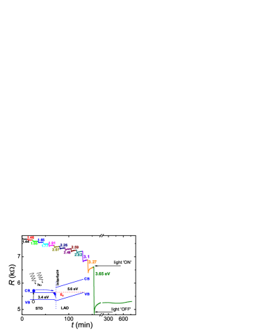
In Fig. 1, we show raw data of the sample resistance as a function of time during light illumination in the energy range between 1.44 and 3.65 eV. Each step corresponds to a constant illumination with a specific energy during 1 minute (light ‘ON’). After illumination, we waited for 10 minutes to allow the resistance to reach a reasonably stable value (light ‘OFF’), before illuminating with the next photon energy. The influence of photons with different energy is clearly seen as a series of steps in the sample resistance. The largest drop in resistance (more than 50%), occurs when the photon energy (3.65 eV) exceeds the STO band gap energy (3.4 eV). This dramatically reduced resistance does not recover to the initial value after the illumination is turned off, and only returns to the previous value when the sample is heated to room temperature. We performed a control experiment on a STO[001] substrate under similar illumination conditions, and found that it remains insulating for all photon energies, which proves that the persistent resistance decrease is a feature of the LAO/STO interface.
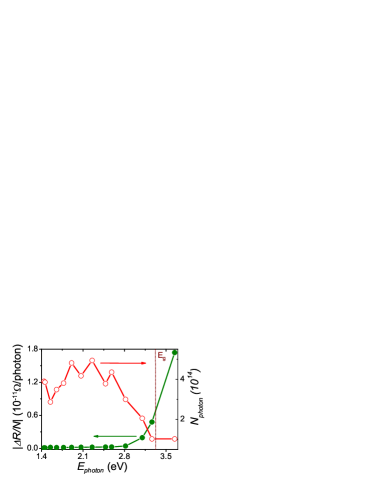
In Fig. 2, we show as open circles (right axis), the variation in the number of illuminating photons as a function of photon energy, which is a consequence of the energy-dependent throughput of the optical set-up. The number of photons at the sample was calculated from the integration over time of the total power incident on the sample, normalized with the energy of a single photon. The solid circles (left axis), show the resistance change of the sample, normalized by the number of incident photons, at each photon energy. The most drastic change occurs when the photon energy is higher than the STO band gap, shown as the vertical dashed line in the figure.
In order to explain these results, we propose the generation of additional, photo-excited carriers, as depicted in the inset of Fig. 1:PRB09Son Illumination with photons of energy greater than the STO band gap creates electron-hole pairs in the STO substrate; the electrons move to the interface potential well, whereas the holes remain trapped in the substrate. Owing to this spatial separation, electron and hole wavefunctions do not overlap and direct optical recombination is suppressed, leading to a persistent resistance change.
To study the nature of the persistent photo-excited carriers, we have performed magnetotransport experiments after illumination with an increasing total number of photons , controlled with neutral density filters, at a constant photon energy of 3.65 eV. In Fig. 3a, we show the Hall resistance as a function of magnetic field at 4.2 K, before illumination and after illuminating with four different values of (open symbols). The corresponding (longitudinal) magnetoresistance are shown in Fig. 3b. Without any illumination, a linear Hall resistance and a small negative magnetoresistance are observed, in agreement with earlier observations on a similar sample.NM07Brink After illumination, a distinctly non-linear Hall resistance and a large positive magnetoresistance appear.
We describe the linear Hall resistance using the conventional single-carrier model, and extract the carrier concentration and mobility from slope of the linear fit to the data - the fit is shown as a solid line in Fig. 3a, where is the applied magnetic field, is the Hall resistance, is the zero field sheet resistance, and is the electronic charge. This yields a carrier density = cm-2 and a mobility = 3 cm2/Vs. This very low carrier-mobility is similar to values previously observed in LAO/STO samples with comparable LAO layer thickness.NM07Brink ; PRB12Her
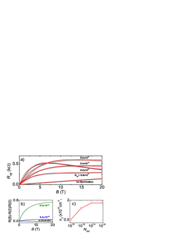
In contrast, the non-linear Hall resistance after illumination cannot be explained within a single-carrier model, but rather suggests a multi-channel system. A similar non-linear Hall resistance was observed previously in LAO/STO,PRB10Kim ; APL10Oht and explained in terms of two-channel conduction from electronic bands with different mobilities, and , and carrier densities, and . We use a similar, simple two-electron-band expression for , given byBCP76Ash
| (1) |
to model our Hall resistance data after illumination.
In this expression, we take and to be the carrier density and mobility of the existing electron band without illumination, and and are the carrier density and mobility of the persistent, photo-excited high mobility band. For low magnetic fields where 1 and 1, and for high magnetic fields where 1 and 1, expression (1) is linear in magnetic field; R(B) becomes non-linear where 1. This simple two-band model is not able to reproduce all the details of the magnetotransport in our sample, but the fact that we observe a non-linear Hall resistance at a few tesla clearly points towards the existence of an optically excited high-mobility channel.
The results of our two-band analysis are shown in Fig. 3a as solid lines. We fitted the non-linear Hall resistance for = , using and as fit parameters, and with fixed values of = cm-2 and = 3 cm2/Vs (as extracted from the linear Hall resistance before illumination): values of = cm-2 and = 1200 cm2/Vs were obtained. For the higher values of we found that the quality of the fits was insensitive to small variations in around this value of 1200 cm2/Vs. We therefore fixed = 1200 cm2/Vs and used only as a fit parameter for the higher values of . The values of extracted in this way are shown in the Fig. 3c. For the highest value of , a good fit to required a slightly increased value of from cm-2 to cm-2, with an unchanged value of (as shown in Fig. 3c). This two-band analysis of the Hall resistance strongly suggests that we populate a second high mobility electron channel by illumination above the STO band-gap.
In summary, we have measured magneto-transport in a LAO/STO heterostructure, with a 10 nm thick LAO film, after illumination with selective photon energy. When the photon energy exceeds the STO band gap, the low-temperature resistance decreases by more than 50% and remains persistent at the lower value. We explain this effect in terms of optical excitation of an additional high mobility electron channel, which is spatially separated from the photo-excited holes, and confirm the presence of a second conducting electron band through measurement of a strongly non-linear Hall resistance after illumination. A two-carrier description of the Hall resistance data after illumination shows one low mobility (3 cm2/Vs) band with a high carrier density ( cm-2) corresponding to the original conduction band present before illumination, and one persistently photo-excited high mobility (1200 cm2/Vs) band with a low carrier density ( cm-2).
This work is part of the InterPhase research program of the Foundation for Fundamental Research on Matter (FOM, financially supported by the Netherlands Organization for Scientific Research (NWO)).
References
- (1) A. Ohtomo and H. Y. Hwang, Nature (London) 427, 423 (2004).
- (2) N. Reyren, S. Thiel, A. D. Caviglia, L. F. Kourkoutis, G. Hammerl, C. Richter, C. W. Schneider, T. Kopp, A. S. Ruetschi, D. Jaccard, M. Gabay, D. A. Muller, J. -M. Triscone, and J. Mannhart, Science 317, 1196 (2007).
- (3) A. Brinkman, M. Van Zalk, J. Huijben, U. Zeitler, J. C. Maan, W. G. Van der Wiel, G. Rijnders, D. H. A. Blank, and H. Hilgenkamp, Nature Mater. 6, 493 (2007).
- (4) M. Ben Shalom, C. W. Tai, Y. Lereah, M. Sachs, E. Levy, D. Rakhmilevitch, A. Palevski, and Y. Dagan, Phys. Rev. B 80, 140403 (2009).
- (5) Ariando, X. Wang, G. Baskaran, Z. Q. Liu, J. Huijben, J. B. Yi, A. Annadi, A. R. Barman, A. Rusydi, S. Dhar, Y. P. Feng, J. Ding, H. Hilgenkamp, and T. Venkatesan, Nature Comm. 2, 7 (2011).
- (6) D. A. Dikin, M. Mehta, C. W. Bark, C. M. Folkman, C. B. Eom, and V. Chandrasekhar, Phys. Rev. Lett. 107, 056802 (2011).
- (7) Lu Li, C. Richter, J. Mannhart, and R. C. Ashoori, Nature Phys. 7, 762 (2011).
- (8) J. A. Bert, B. Kalisky1, C. Bell, M. Kim, Y. Hikita, H. Y. Hwang, and K. A. Moler, Nature Phys. 7, 767 (2011).
- (9) M. Ben Shalom, A. Ron, A. Palevski, and Y. Dagan, Phys. Rev. Lett. 105, 206401 (2010).
- (10) A. D. Caviglia, S. Gariglio, C. Cancellieri, B. Sacepe, A. Fete, N. Reyren, M. Gabay, A. F. Morpurgo, and J. -M. Triscone, Phys. Rev. Lett. 105, 236802 (2010).
- (11) A. McCollam, S. Wenderich, M. K. Kruize, V. K. Guduru, H. J. A. Molegraaf, M. Huijben, G. Koster, D. H. A. Blank, G. Rijnders, A. Brinkman, H. Hilgenkamp, U. Zeitler, and J. C. Maan e-print arXiv:1207.7003[cond-mat.mtrl-sci].
- (12) N. Nakagawa, H. Y. Hwang, and D. A. Muller, Nature Mater. 5, 204 (2006).
- (13) K. Yoshimatsu, R. Yasuhara, H. Kumigashira, and M. Oshima, Phys. Rev. Lett. 101, 026802 (2008).
- (14) M. Sing, G. Berner, K. Goß, A. Müller, A. Ruff, A. Wetscherek, S. Thiel, J. Mannhart, S. A. Pauli, C. W. Schneider, P. R. Willmott, M. Gorgoi, F. Schäfers, and R. Claessen, Phys. Rev. Lett. 102, 176805 (2009).
- (15) W. Siemons, G. Koster, H. Yamamoto, W. A. Harrison, G. Lucovsky, T. H. Geballe, D. H. A. Blank, and M. R. Beasley, Phys. Rev. Lett. 98, 196802 (2007).
- (16) G. Herranz, M. Basletić, M. Bibes, C. Carretero, E. Tafra, E. Jacquet, K. Bouzehouane, C. Deranlot, A. Hamzić, J.-M. Broto, A. Barthelemy, and A. Fert, Phys. Rev. Lett. 98, 216803 (2007).
- (17) P. R. Willmott, S. A. Pauli, R. Herger, C. M. Schlepütz, D. Martoccia, B. D. Patterson, B. Delley, R. Clarke, D. Kumah, C. Cionca, and Y. Yacoby, Phys. Rev. Lett. 99, 155502 (2007).
- (18) M. Huijben, A. Brinkman, G. Koster, G. Rijnders, H. Hilgenkamp, and D. H. A Blank, Adv. Mater. 21, 1665 (2009).
- (19) C. Bell, S. Harashima, Y. Hikita, and H. Y. Hwang, Appl. Phys. Lett. 94, 222111 (2009).
- (20) F. J. Wong, R. V. Chopdekar and Y. Suzuki, Phys. Rev. B 82, 165413 (2010).
- (21) A. Rastogi, A. K. Kushwaha, T. Shiyani, A. Gangawar, and R. C. Budhani, Adv. Mater. 22, 4448 (2010).
- (22) A. Rastogi, J. J. Pulikkotil, S. Auluck, Z. Hossain, and R. C. Budhani, Phys. Rev. B 86, 075127 (2012).
- (23) A. Tebano, E. Fabbri, D. Pergolesi, G. Balestrino, and E. Traversa, AcsNANO 6, 1278 (2012).
- (24) G. Koster, B. L. Kropman, G. J. H. M. Rijnders, D. H. A. Blank, and H. Rogalla, Appl. Phys. Lett. 73, 2920 (1998).
- (25) W.-j. Son, E. Cho, B. Lee, J. Lee, and S. Han, Phys. Rev. B 79, 245411 (2009).
- (26) T. Hernandez, C. W. Bark, D. A. Felker, C. B. Eom, and M. S. Rzchowski1, Phys. Rev. B 85, 161407 (2012).
- (27) J. S. Kim, S. S. A. Seo, M. F. Chisholm, R. K. Kremer, H. U. Habermeier, B. Keimer, and H. N. Lee, Phys. Rev. B 82, 201407 (2010).
- (28) R. Ohtsuka, M. Matvejeff, K. Nishio, R. Takahashi, and M. Lippmaa, Appl. Phys. Lett. 96, 192111 (2010).
- (29) N. W. Ashcroft and N. D. Mermin, Solid State Physics (Harcourt Brace College Publishers, 1976) page number 240.