Gate-induced carrier density modulation in bulk graphene: Theories and electrostatic simulation using Matlab pdetool
Abstract
This article aims at providing a self-contained introduction to theoretical modeling of gate-induced carrier density in graphene sheets. For this, relevant theories are introduced, namely, classical capacitance model (CCM), self-consistent Poisson-Dirac method (PDM), and quantum capacitance model (QCM). The usage of Matlab pdetool is also briefly introduced, pointing out the least knowledge required for using this tool to solve the present electrostatic problem. Results based on the three approaches are compared, showing that the quantum correction, which is not considered by the CCM but by the other two, plays a role only when the metal gate is exceedingly close to the graphene sheet, and that the exactly solvable QCM works equally well as the self-consistent PDM. Practical examples corresponding to realistic experimental conditions for generating graphene pnp junctions and superlattices, as well as how a background potential linear in position can be achieved in graphene, are shown to illustrate the applicability of the introduced methods. Furthermore, by treating metal contacts in the same way, the last example shows that the PDM and the QCM are able to resolve the contact-induced doping and screening potential, well agreeing with the previous first-principles studies.
pacs:
73.22.Pr 85.30.De 72.80.Vp 41.20.Cv1 Introduction
Electronic transport in graphene CastroNeto2009 ; DasSarma2011 , a one-atom-thick honeycomb carbon lattice, is one of its main issues among the increasing number of fundamental studies ever since the first successful isolation of stable monolayer graphene flakes in 2004 Novoselov2004 . What led to the explosive growth of the graphene literature, however, was not only the discovery of the mechanical exfoliation (Scotch-tape method) for graphene flake preparation, which made graphene easily accessible to laboratories all over the world, but also the characterization of the electronic properties of graphene by electrical gating, which provides a direct way to modulate the carrier density, and hence the Fermi level, of graphene Novoselov2004 . Conductance (resistance) sweep using a single backgate is henceforth a standard electronic characterization tool for graphene. Double-gated graphene opens even more possibilities of graphene electronics and allows experimental studies of graphene pn and pnp junctions Huard2007 ; Williams2007 ; Ozyilmaz2007 ; Liu2008c ; Gorbachev2008 , as well as the interesting physics of Klein tunneling Cheianov2006 ; Katsnelson2006 ; Stander2009 ; Young2009 ; Nam2011 . Gate-induced carrier density modulation, therefore, plays an essential role for fundamental as well as advanced studies of graphene electronics.
Theory of the gate-induced carrier density modulation is mainly an electrostatic problem. How one should obtain the gate-voltage dependence of the carrier density in graphene depends actually on how precise one wishes. For cheapest computation, the graphene sheet carrier density can be directly regarded as the induced surface charge density adjacent to graphene Novoselov2004 , which is treated as a conductor fixed at zero potential. This corresponds to the classical capacitance model (CCM) that is widely adopted in most experimental works on graphene transport DasSarma2011 and can be solved exactly. A more precise computation takes into account the relation between the induced charge density on graphene and the electric potential energy that those charge carriers gain, through the graphene density of states Guo2007 ; Fern'andez-Rossier2007 ; Fang2007 . This requires self-consistent iterative computation Gorbachev2008 ; Shylau2009 ; Andrijauskas2012 , which is a bit more expensive, but actually corresponds to the quantum capacitance model (QCM) Luryi1988 , within which exact solutions for single-gated pristine graphene Fang2007 and even multigated doped graphene Liu2013 can be obtained. Further considerations such as the Coulomb interaction of the induced charges on the graphene sheet are possible Fern'andez-Rossier2007 ; Shylau2009 , but these would be out of the scope of the present discussion.
Whereas a thorough and comprehensive review on the theory of gate-induced carrier density modulation of bulk graphene so far does not exist in the literature, part of this article aims at providing this missing piece. The review includes both the analytical and numerical aspects, as well as a brief introduction to the usage of Matlab’s pdetool, in order for a self-contained context. Readers who happen to be Matlab users would find this brief usage helpful, but non-Matlab users may as well neglect it without encountering further gaps. The analytics based on the CCM and QCM and the numerics based on the self-consistent iteration method, namely, the Poisson-Dirac method (PDM), using Matlab’s pdetool will be compared, showing that the quantum correction plays usually a minor role, unless the metal gate is exceedingly close to the graphene sheet. In the case of single-gated pristine graphene, consistency between the QCM and PDM is satisfactory even for capacitors with finite gates, and is exact for parallel-plate capacitors with infinitely extending gates.
With a full understanding of the gate-voltage modulation on the graphene carrier density, examples of its applications aiming at providing realistic local energy band offsets due to electric gating will be illustrated. This is particularly important for an accurate theoretical modeling of transport in graphene Liu2012a . Examples include (i) graphene pnp junctions, (ii) graphene superlattices, and (iii) generation of background potential linear in position in graphene. Practically, the example (i) provides the study of the physics of Klein backscattering Shytov2008 ; Young2009 ; Liu2012a , while the combination of the examples (ii) and (iii) is the underlying prerequisite of the Bloch-Zener oscillation in graphene Krueckl2012 . Furthermore, the introduced PDM and QCM are capable of treating the effects of metal contacts, for which example (iv) of contact-induced doping and screening potential is also illustrated. Taking palladium as a specific example of the metal contact, the results obtained by the PDM and QCM are shown to agree well with the previous first-principles studies Khomyakov2009 ; Khomyakov2010 .
This paper is organized as follows. In Sec. 2, we first provide a brief introduction to the usage of Matlab’s pdetool, pointing out the least knowledge required to apply the tool on the present specific electrostatic problem. Theories of the gate-induced carrier density modulation in graphene are reviewed in Sec. 3, where the analytics based on the capacitance models and the numerics based on the PDM is also compared. Practical applications based on the theories reviewed in Sec. 3 are given in Sec. 4, and a summary of the present work is concluded in Sec. 5.
2 Usage of Matlab’s pdetool for electrostatics
The pdetool is a useful numerical tool built in Matlab and provides a convenient way to solve several classic partial differential equation (PDE) problems in two-dimension. For the electrostatics at our present interest, the Poisson equation,
| (1) |
obtained from two of the Maxwell’s equations, and , which respectively lead to and , is the central equation that the pdetool solves for the electric potential .111To be consistent with the pdetool, we name the electric potential as , while reserve the variable for the energy band offset (the “on-site energy” in the language of tight-binding formulation). In Eq. (1), the product of the dielectric constant (relative permittivity) and the free space permittivity gives the absolute permittivity .
A full introduction to the usage of the pdetool can be found in the Matlab documentation pde and need not be repeated here. To digest the full user’s guide of the tool, however, is not necessary for our present focus, which is essentially an electrostatic problem. This section is basically to elaborate those that are less clear in pde but nevertheless important for our purpose of obtaining the gate-voltage dependence of the graphene carrier density, and to point out the least required knowledge for this purpose.
2.1 Overview of pdetool
To solve a PDE problem using the pdetool, required necessary inputs can be exported from the graphical user interface (GUI) of the pdetool (initiated by executing “pdetool” from the command window) and are briefly described in the following.
-
(i)
System geometry. The geometrical shapes of the building blocks, such as the oxide layers, metallic gates, etc., which constitute the system where the PDE problem is defined, can be drawn in the “Draw Mode” of the GUI. The resulted “decomposed geometry” allows us to proceed to the rest of the inputs, but there is no need to “Export Decomposed Geometry, Set Formula, Labels…” from the “Draw menu” since not all of them will be needed by the PDE solvers.
-
(ii)
PDE coefficients. In the “PDE Mode” of the GUI, one can designate different regions of materials by filling in the respective dielectric constants and space charge densities. These are stored in certain PDE coefficients matrices, which can be output from the GUI and will be required by the PDE solvers in programming.
-
(iii)
Boundary conditions. In the “Boundary Mode” of the GUI, boundary conditions for each bounding edge can be assigned. The resulting boundary matrix , which will be required by the PDE solvers in programming, and the Decomposed Geometry, which will be required when visualizing the PDE geometry, can be exported from the “Boundary menu”. An elaborated instruction about will be given later.
-
(iv)
Mesh points. The mesh points are those spatial points at which the numerical solutions are desired. They can be created, refined, or jiggled in the “Mesh Mode” of the GUI. The resulting triangular mesh data, stored by point, edge, and triangle matrices, can be exported by the GUI and will be used not only when calling for the PDE solvers but also when visualizing the solution.
With all these requirements completed, the PDE problem is then defined, and the solution can as well be obtained by clicking “Solve PDE” within the GUI, which is user-friendly but cannot be “programmed”. When performing certain real calculations, however, especially when a systematic change of variables is required, programming with, e.g., looping, is inevitable and the requirements of (ii)–(iv) will be the necessary inputs of the PDE solvers. For our purpose of simulating the carrier density modulation due to gating, we would often need to change the gate voltages, which are described by the boundary conditions. Thus although each of (ii)–(iv) can be programmed by using relevant commands, in the following only the implementation of (iii) by commands will be described in detail.
2.2 Boundary conditions
2.2.1 The boundary condition matrix: General description
By searching “assemb” from the Matlab help or by looking up in its documentation pde , we see that the boundary conditions are saved in a matrix called , with the following data format:
-
•
Row contains the dimension of the system. (Note: normally . If one solves two coupled variables, then etc.; by examining the exported boundary condition matrix , one would find that for inner boundaries.)
-
•
Row contains the number of Dirichlet boundary conditions.
-
•
Rows to contain the lengths for the strings representing . The lengths are stored in columnwise order with respect to . [See Eq. (2) below.]
-
•
Rows to contain the lengths for the strings representing . [See Eq. (2) below.]
-
•
Rows to contain the lengths for the strings representing . The lengths are stored in columnwise order with respect to . [See Eq. (3) below.]
-
•
Rows to contain the lengths for the strings representing . [See Eq. (3) below.]
-
•
The following rows contain text expressions representing the actual boundary condition functions.
Here, two types of boundary conditions222The mixed type boundary conditions will not be encountered in the present discussion. are included, namely, the Neumann boundary
| (2) |
and the Dirichlet boundary
| (3) |
In Eq. (2), contains the PDE coefficients (here the dielectric constants in different regions), and is the normal of the boundary. So the boundary conditions for given gate voltages would be the Dirichlet type, with and being the corresponding voltage. For the Neumann type boundary condition, we normally consider , and represents the surface charge.
In the following, let us be more specific about the format of the boundary conditions matrix, considering the two types of boundaries with .
2.2.2 Dirichlet boundary
Following the general description of Sec. 2.2.1, the boundary matrix for a Dirichlet boundary is described as follows.
-
•
Row contains the dimension of the system:
-
•
Row contains the number of Dirichlet boundary conditions:
-
•
Row contains the length for the strings representing , which is since , though not used.
-
•
Row contains the length for the strings representing , which is since , though not used.
-
•
Row contains the length for the strings representing , which is since .
-
•
Row contains the length for the strings representing .
-
•
Then comes the text expressions of .
An example of a Dirichlet boundary with would be:
| b = [1 1 1 1 1 3 ’0’ ’0’ ’1’ ’3.5’]’; |
The boundary condition may include the and position coordinates and their functions, and can be written even in terms of the solution (nonlinear solver required). For example,
| b = [1 1 1 1 1 4 ’0’ ’0’ ’1’ ’x.^2’]’; |
For another example,
| b = [1 1 1 1 1 9 ’0’ ’0’ ’1’ ’sin(x).^u’]’; |
2.2.3 Neumann boundary
Following the general description of Sec. 2.2.1, the boundary matrix for a Neumann boundary is described as follows.
-
•
Row contains the dimension of the system: .
-
•
Row contains the number of Dirichlet boundary conditions: .
-
•
Row contains the length for the strings representing , which is since .
-
•
Row contains the length for the strings representing .
-
•
Then comes the text expressions of .
An example of a Neumann boundary with surface charge would be
| b = [1 0 1 3 ’0’ ’1.6’]’; |
Another example
| b = [1 0 1 21 ’0’ ’-13.295*sign(u).*u.^2’]’; |
will actually be used when we apply the Poisson-Dirac iteration method.
2.2.4 Text expression of the boundary conditions
The boundary condition matrix exported from the GUI of the pdetool looks filled with purely integers. This is the “number representation” of the text strings. For example, a number within the matrix actually means ‘0’:
>> char(48) ans = 0
Conversely, if we want to transform the strings into numbers, we can simply use the ‘double’ command:
>> double(’x.^2’) ans = 120 46 94 50
Thus to enter a boundary condition of, e.g., , we may fill in with:
| double(’-(x.^2+y.^2)’)’ |
To enter a Dirichlet boundary condition of a given number assigned by a variable named Vtg, we may fill in with:
| double(num2str(Vtg))’ |
Note that the operator ’ at the end of these two examples is to take transpose of the converted text strings, since the boundary conditions are saved columnwise in , and similarly in the previous examples for .
For a real PDE problem, the number of columns of the matrix depends on the total number of edges, including inner and outer boundaries. The th column records the boundary condition for the th edge. Thus before exporting the initial matrix from the GUI of pdetool, one has to check the boundary labels corresponding to, e.g., graphene or gates (by showing the edge labels in the “Boundary Mode”).
2.3 Some important commands
2.3.1 Solving the PDE
A standard PDE solver is called assempde. An example for its usage is as follows.
u = assempde(b,p,e,t,c,a,f); % b: matrix of boundary conditions % p: points of the mesh grid % e: edges % t: triangles % c,a,f: coefficients of the pde problem
When the solution is involved in the boundary conditions, the solution mode has to be switched to nonlinear. An example for its usage is as follows.
[u,res] = pdenonlin(b,p,e,t,c,a,f, ...
’report’,’on’,’MaxIter’,1e5,’u0’,u0);
% u: the solution, res: not important here
% b,p,e,t,c,a,f: same as above
% ’report’:iteration process report
% ’MaxIter’: maximal number of iter. rounds
% ’u0’: initial guess of the solution
2.3.2 Interpolation
To find the values at those points one desires, an important command called tri2grid should be used, which interpolates from the PDE triangular mesh to a given rectangular grid. An example for usage is as follows.
uxy = tri2grid(p,t,u,x,y); % u: the obtained solution % p,t: same as above % x,y: rectangular grid points for interpol.
2.4 Remarks on units
In the pdetool, everything is displayed with dimensionless numbers. The actual units can be chosen as what we would like. Deducing relevant coefficients for a specific set of chosen units is therefore important before we use the pdetool to solve any actual problems.
In addition to the physical units, the free space permittivity is suppressed throughout the program. Recall the boundary conditions for the displacement field at a conductor-dielectric boundary, which can be derived by applying the Gauss’s law: and , where and represent the components tangential and normal to the interface, respectively. The normal component of the displacement field therefore means the surface charge density:
| (4) |
Comparing Eq. (4) to Eq. (2) with and representing (instead of ), one can see that the “Surface charge” actually means
| (5) |
when filling the Neumann boundary condition in the “Boundary Mode” of the GUI. Similarly, when filling the PDE coefficients in the “PDE Mode”, the “Space charge density” actually means rho , i.e., the right-hand side of Eq. (1).
3 Theories of gate-induced carrier density modulation
In this section, analytical theories of the gate-induced carrier density modulation, including the classical and quantum capacitance models, are briefly reviewed, a numerical scheme of the self-consistent Poisson-Dirac iteration method is introduced, and a numerical comparison between analytics and numerics is provided.
3.1 Classical capacitance model
3.1.1 The model
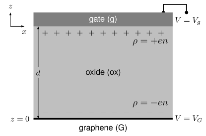
We begin with the classical capacitance model, which considers a parallel-plate capacitor composed of an oxide dielectric with permittivity sandwiched by a metallic gate (at ) and a conducting graphene sheet (at ) as sketched in Fig. 1. Let the electric potential at the gate be and the graphene layer be grounded: . The surface charge density at (the surface of the oxide dielectric in contact with the graphene layer) from Eq. (4) is given by
| (6) |
where is the classical capacitance (per unit area) of a uniform parallel-plate capacitor. Regarding this surface charge (6) directly as those induced carriers in the graphene layer, we have the carrier density
| (7) |
which is a widely used formula for estimating the graphene carrier density DasSarma2011 . For uniform capacitors with , Eq. (7) numerically reads
| (8) |
where and are in units of V and nm, respectively.


3.1.2 Using pdetool
The Dirichlet boundary conditions
| (9) |
can be straightforwardly implemented in the pdetool.333If a uniform capacitor (without dependence) is desired, one needs to assign Neumann boundary conditions at the left and right sides of the oxide boundaries with vanishing surface charge density , which forces the displacement field to be tangential (normal) to the side (top and bottom) boundaries. The standard PDE solver assempde introduced in Sec. 2.3 should be chosen. Working with units and , the carrier density (7) is numerically given by
| (10) |
Note that the interpolation command tri2grid introduced in Sec. 2.3 may be useful in performing the numerical derivative at .
3.1.3 Remark on the gate-induced Rashba spin splitting
At this stage we may also estimate for graphene the gate-induced Rashba spin splitting, an intrinsic coupling between the spin and orbital degrees of freedom of charge carriers in a two-dimensional conducting plane subject to a perpendicular electric field Rashba1960 ; Bychkov1984 . In graphene, the Rashba spin splitting has been shown by first principles to exhibit a linear dependence on the electric field Gmitra2009 ; Abdelouahed2010 : , where is the electric field strength perpendicular to graphene given in units of . If the graphene carrier density stems from gating and is classically given by , the corresponding surface charge density , in fact, has already revealed the displacement field on itself, allowing us to express the Rashba spin splitting in terms of the carrier density,
| (11) |
where is in units of , a typical order of the graphene carrier density.
This estimation indicates that the Rashba spin splitting induced solely by electric gating typically lies in the order of eV, which may hinder the observation of those interesting physics based on the Rashba spin-orbit coupling in graphene, such as the interfacial spin and charge currents Yamakage2011 ; Tian2012 , or the spin-dependent Klein tunneling Yamakage2009 ; Liu2012 . The position dependence of the Rashba coupling across a pn junction interface Rataj2011 , on the other hand, can be accurately taken into account by putting the -dependence of (or even ) in Eq. (11). A stronger Rashba spin splitting in graphene is therefore less possible by gating, but may be achieved by, for example, using a ferromagnetic substrate with an intercalated gold monolayer Sanchez-Barriga2010 .
3.2 Self-consistent Poisson-Dirac iteration method
From Eq. (6) to Eq. (7), the assumption that “the induced surface charge density at the dielectric surface is the graphene carrier density” obviously have neglected a few physical details, such as the graphene density of states that govern the statistics of how the states in graphene should be filled by the carriers accordingly. In addition, filling the carriers into graphene causes the change of its Fermi level, implying a potential energy shift that should further correspond to the electric potential times the electron charge. These are what the classical capacitance model have neglected and what the following Poisson-Dirac iteration method is going to compensate.
3.2.1 Basic idea
Consider a pristine graphene with Fermi level lying exactly at the charge neutrality point, i.e., the Dirac point . Application of the gate voltage induces a certain amount of additional charges on graphene, , which occupy the states in graphene according to its density of states (within the Dirac model):
| (12) |
where is the Fermi velocity of graphene. A positive (negative) electron number density raises (lowers) the Fermi level from to . On the other hand, the electron at the Fermi level, which is responsible for transport in the linear response regime, gains an energy from the electric field, where is the electron charge444Throughout this paper, is the positive elementary charge. and is the electric potential at the graphene sheet obtained by solving the Poisson Eq. (1). This potential energy , which is equivalent to the “on-site energy” in the tight-binding transport formulation (see, for example, Liu2012a ), will raise the whole band structure, and thus lower the Fermi level by the same amount. We can therefore legitimately put
| (13) |
into Eq. (12), leading to
| (14) |
The surface charge density at the graphene layer is now expressed in terms of the solution , but is at the same time the Neumann boundary condition that influences the numerical solution to the Poisson equation. This formally makes the solution process iterative.
3.2.2 Using pdetool
The Dirichlet boundary condition (9) for the gate boundary remains valid, while that for the graphene boundary has to be modified to the Neumann type:
| (15) |
where is given by Eq. (14). Working with units and together with , Eq. (14) becomes
| (16) |
which should be keyed as “-13.295*sign(u).*u.^2” in the boundary condition matrix, noting that the solution in the pdetool is by default named . The nonlinear solver pdenonlin introduced in Sec. 2.3 has to be chosen in this case, where the solution is involved in the boundary conditions, and the iteration will be automatically processed by the pdetool.
Once the solution , and hence the electrostatic potential at the graphene layer , is iteratively obtained, the desired carrier density profile can then be expressed in terms of :
| (17) |
which follows from Eqs. (12) and (13). Note that we have added explicitly a subscript “PD” in Eq. (17) to distinguish with the classical contribution, .
3.3 Quantum capacitance model
The relation between the induced charge density on graphene and the electric potential energy that those charge carriers gain through the graphene density of states is taken into account by the PDM, with a price of iteration process paid. For single-gated graphene, there is an alternative that can take this into account analytically: the quantum capacitance model Luryi1988 , which we briefly review here for bulk graphene following the work of Fang2007 .555For the general case of multigated doped graphene, see Liu2013 . The derivation is similar, and the review here is restricted to the simple case of single-gated pristine graphene.
3.3.1 The model
The single-gated graphene shown in Fig. 1 is treated by the equivalent circuit plot as shown in Fig. 1, where an additional capacitor is inserted between the voltage point and the ground, as contrary to the CCM, Fig. 1. As Fig. 1 suggests , using we have
| (18) |
Following the same physics stated in Sec. 3.2.1, the carrier density at the graphene layer, i.e., Eq. (14) divided by , is expressed in terms of the electric potential thereof as
| (19) |
Equating (18) and (19), one obtains a quadratic equation for ,
| (20) |
Solving Eq. (20) for and putting back to Eq. (18), the graphene carrier density can be written as
| (21) |
where given by Eq. (7) is the classical contribution, and
| (22) |
with definition
| (23) |
corresponds to the quantum correction.666Note that Eqs. (21)–(23) (with ) were first derived in Fang2007 and reviewed in DasSarma2011 , but a factor of in the square root of the formula (1.15) in DasSarma2011 , corresponding to Eq. (22) here, is missing.
Furthermore, by comparing Eq. (21) with Eq. (18), one can also write down the solution for the electric potential on graphene:
| (24) |
which has a reasonable form of charge divided by capacitance. The “charge” in Eq. (24) contains only the quantum correction as expected, since the classical solution, which regards graphene as a grounded conductor, does not contribute to the potential .
3.3.2 Quantum correction for parallel-plate capacitors
For parallel-plate capacitors with uniform dielectrics, the capacitance is well known to be , such that Eq. (23) and hence the quantum correction (22) are solely determined by the classical contribution . In this case we can further express Eq. (23) as , where is in units of nm and is again adopted. Together with Eq. (8), the quantum correction given by Eq. (22) can be written as
| (25) |
where is in units of V and has been substituted. We will soon see that this correction derived within the analytical QCM for an infinitely extending parallel-plate capacitor will exactly correspond to that by the numerical PDM.
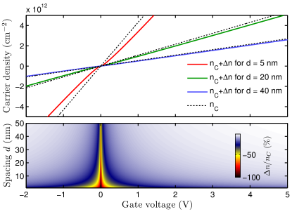
To give an overview of how much change the quantum correction causes as compared to the classical , we plot in the upper panel of Fig. 2 the carrier density, with and without , as a function of , considering oxide thickness with of the assumed dielectric SiO2. Apparently, only when is extremely thin can one see a clear difference due to (). With nonzero and large , one can further approximate Eq. (25) as
| (26) |
which shows a rapid decay of with to the power of .
In the opposite limit of vanishing and thin , however, the magnitude of may become comparable with . In the lower panel of Fig. 2, the ratio is plotted as a function of and . As expected, in the region away from and , the ratio is close to zero, meaning a minor role played by the quantum correction. Contrarily, the ratio grows significantly when approaching to the and axes,777The ratio further diverges to at , but at this axis both and vanish, and is strictly speaking undefined. implying an important role played by the quantum correction.
3.3.3 Remark on quantum capacitance
Note that the appearance of stems from the finite density of states provided by the conducting layer for the electrons to occupy following the quantum nature of the Pauli exclusion principle, and hence the name quantum capacitance Luryi1988 , which is not restricted to the material graphene. The expression of for graphene Fang2007 , however, is not important for the present discussion. Instead, leads to a quantum correction to the gate-induced carrier density , which is the main focus here.
In addition, recent experimental progress on the measurement of graphene quantum capacitance Xia2009 ; Droscher2010 ; Ponomarenko2010 suggests that the electron-hole puddles Martin2008 induced by charged impurities may influence at energies close to the charge neutrality point. The corresponding carrier density fluctuation , which can be considered to develop a microscopic model to account for the smoothing of the graphene quantum capacitance at the charge neutrality point Xu2011 , is beyond the scope of the present discussion.
3.4 Analytics vs numerics
The two analytical capacitance models and the numerical scheme of the Poisson-Dirac iteration method are compared in the following, considering a single-gated graphene with individually infinite and finite size of the gate.
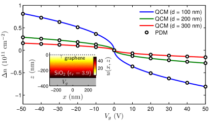
We start with uniform parallel-plate capacitors as those considered in Sec. 3.3.2 with different spacings nm. Schematic of the capacitor with is sketched in the inset of Fig. 3, where the electric potential within the oxide layer is obtained by the PDM at .888Note that the spatial profile of the electric potential , with the quantum correction on graphene taken into account, does not look too much different compared to the classical solution , where the graphene layer is assumed to be grounded. The difference of them at , however, is crucial since the latter is always zero, i.e., . The classical contribution is first computed following Sec. 3.1.2 [which gives the same result with Eq. (8)], and the quantum correction is computed in two ways. For the analytical QCM, Eq. (25) is used to compute . For the numerical PDM, the full carrier density is computed following Sec. 3.2.2, and the correction is given by the difference . As shown in Fig. 3, the correspondence between the two approaches is exact.
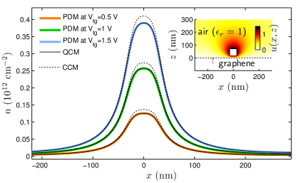
Next we consider a finite-size suspended topgate (such as those fabricated in Liu2008c ; Gorbachev2008 ) with various voltages and an extremely narrow spacing nm; see the inset of Fig. 4. The calculations are similar to those for the infinite case described above. The only difference is the approximating form of the dielectric capacitance,
| (27) |
from which given by Eq. (23) and hence the quantum correction, Eq. (22) from the analytical QCM, is obtained. In Fig. 4, we compare the carrier densities calculated by the PDM, , the QCM, , as well as the CCM, . Good agreement between PDM and QCM is again clearly seen, while the deviation of the CCM from them is observable due to the rather thin spacing between the gate and the graphene sheet.
From the above testing calculations (Figs. 3 and 4), we may conclude that the QCM is equivalent to the PDM in both cases of infinite (uniform) and finite (nonuniform) gate-graphene capacitors. In particular, the correspondence between the two approaches in the former case is exact, while the discrepancy in the latter is merely negligible, suggesting that Eq. (27) is a good approximation for calculating the spatially varying oxide capacitance that further determines the quantum correction given by Eq. (22) through the definition (23) within the QCM. The classical solution for the nonuniform case [following Sec. 3.1.2], therefore, serves as the preliminary solution step for the exactly solvable QCM, circumventing the self-consistent iteration during the solution process that is needed in the PDM.
3.5 Beyond single-gated pristine graphene
The above discussion considers only single-gated graphene in the absence of chemical doping. For double-gated graphene with topgate and backgate at two sides of the graphene sheet, the two gates can be regarded as independent, and their contributions to the carrier density modulation can be treated separately and superposed to yield the total carrier density. When multiple gates are acting on the graphene sheet from the same side, however, such as using an embedded local gate in addition to a global backgate to create pnp junctions with independent control of the globally and locally gated regions Nam2011 (see Sec. 4.2), or patterned topgates that may generate a graphene superlattice (see Sec. 4.3), these gates should be simultaneously treated.
In fact, the CCM (Sec. 3.1.2) as well as the PDM (Sec. 3.2.2) are not restricted to the case of single-gated graphene. These two approaches work for any kind of gating geometry, provided that the boundary conditions [Eq. (9) for CCM and Eq. (15) for PDM] at the graphene layer are properly assigned. The applicability of the QCM of the presently reviewed version, however, depends then on the gating geometry. When multiple gates are acting on graphene from the same side but connected to each other to share the same gate voltage (as the case of Sec. 4.3), there is effectively only one gate. In this case, Eq. (27) is still a good approximation to account for the oxide capacitance, and the QCM can be directly applied. On the other hand, if the multiple gates can be separately controlled (as the case of Sec. 4.2), Eq. (27) becomes insufficient due to the need of multiple self-partial capacitances, and the QCM (of the presently reviewed version) cannot be applied. Generalization of the model to take into account composite gating geometry has been recently achieved Liu2013 , but is beyond the scope of the present review.
4 Applications
A successful simulation for electronic transport in bulk graphene relies on not only sophisticated computation techniques but also a realistic “potential profile” that is experimentally relevant Liu2012a . The term “potential” refers to the local potential energy added to the system Hamiltonian when modeling for graphene electronic transport. Thus the potential profile simply means the local energy band offset of the graphene sheet subject to a spatially varying carrier density due to electrical gating. This section is devoted to the application of the carrier density calculation: the corresponding potential profile, or the local energy band offset, which is a simple computational task but nevertheless important for graphene electronic transport calculations. A few concrete examples will be illustrated, after a short review of the potential profile is given.
4.1 Potential profile (local energy band offset)
In Sec. 3 we have introduced how to compute with a satisfactory accuracy the graphene carrier density , which is related to the quasi-Fermi level through Eq. (12) as . The energy band offset then reads , where is the global Fermi level. Choosing (as is usually the case and will be adopted in the rest of the calculations), the space-resolved band offset reads Liu2012a
| (28) |
which is termed on-site energy in the tight-binding formulation for transport calculations.
Equation (28) interprets the carrier density profile in terms of the potential profile , and is valid for computed by either CCM, QCM, or PDM. It should be remarked, however, that the Poisson-Dirac iterative solution to the electric potential at the graphene layer times readily gives the desired energy band offset, and Eq. (28) is not needed within this approach. Likewise in the QCM, is given by Eq. (24) and its product with also gives the desired . Thus within QCM and PDM, one does not need to bother with Eq. (28) for obtaining the potential profile. Contrarily, the CCM always treat the graphene sheet as a grounded conductor and therefore needs the interpretation (28). In other cases where PDM is partly used but the total carrier density is separately computed (such as Sec. 4.3), one needs Eq. (28) as well.
4.2 Graphene pnp junctions
We begin the illustrative examples with a graphene pnp junction, using a global backgate and an embedded local gate. The gating geometry is sketched in Fig. 5, similar to those experimentally fabricated in Nam2011 . In this case both of the global and local gates influence the graphene carrier density from the same side, and therefore have to be treated at the same time. As remarked previously in Sec. 3.5, the single-gate version of the QCM does not apply here,999The multigate version of the QCM Liu2013 , which requires to compute the self-partial capacitances and due to respectively the local gate and the backgate, can be shown to yield results well agreeing with the PDM. but nevertheless can be used to estimate the quantum correction due to the embedded local gate at the region above it. Here we will mainly compare the results from the CCM and those from the PDM, fixing the local gate voltage at while varying the backgate voltage with .

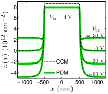
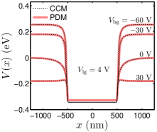
The computed carrier densities are shown in Fig. 5, where the Poisson-Dirac solution agrees well with the simulation presented in Nam2011 . Since the local gate is embedded only below the graphene sheet, the quantum correction excluded in the CCM becomes pronounced within the locally gated region, and can be estimated by Eq. (25) of the QCM. At the center of the locally gated region, the electric field generated by the backgate is almost completely screened, and the classical contribution to the carrier density can be estimated by , leading to and hence , which is pretty close to from the data of Fig. 5 for all .
The carrier density profiles of Fig. 5 are translated into via Eq. (28), as shown in Fig. 5. The positive charges the locally gated graphene with a positive number of electrons, forming an n-type region with positive quasi-Fermi level that is equivalent to applying a negative energy band offset . Outside the locally gated region, the carrier type of graphene is controlled by the backgate with a similar principle. The most interesting feature here is that the locally gated region can be controlled independently due to the screening of the embedded local gate, as is evident in both Figs. 5 and 5. This independent control leads to the four quadrants of the conductance map with two boundaries perpendicular to each other Nam2011 , as contrary to those observed in top-gated devices Huard2007 ; Williams2007 ; Ozyilmaz2007 ; Liu2008c ; Gorbachev2008 ; Stander2009 ; Young2009 .
4.3 Graphene superlattices
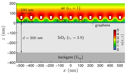
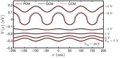
Next we turn to the possibility of generating a graphene superlattice by fabricating a series of patterned topgates. As sketched in Fig. 6, the PDE problem is defined within the region above the graphene sheet in order to solve the electric potential due to the topgates with various voltages . The contribution from the backgate is assumed to be uniform and can be treated independently. The strategy here is to compute first the carrier density due to topgates, and then include the backgate contribution to yield the total carrier density that finally gives the energy band offset profile from Eq. (28). In this case the approximation (27) for the QCM is rather acceptable, and we will compare the results from all of the three approaches.
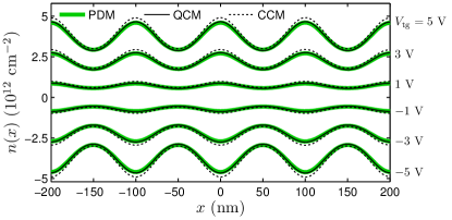
The computed carrier densities by PDM, QCM, and CCM are shown in Fig. 6. The curves of and almost coincide with each other. The relatively thick of Al2O3 suppresses the quantum correction to a reasonably small amount, such that here the CCM is not a bad approximation, either. The discrepancy between and (or ) is less pronounced at the regions between each adjacent pair of topgates since the quantum correction roughly decreases with the -th power of the distance to the gate, as mentioned in Eq. (26).
The carrier density modulation follows the patterned topgates with a periodicity of , giving rise to a periodic potential profile as shown in Fig. 6, where a backgate contribution with is taken into account. Since is related to through a square-root relation, Eq. (28), the shape of can be a bit different from that of , which is similar to a sine-like wave, especially for those that alternate between positive and negative values. Note that the backgate voltage chosen in Fig. 6 results in a rather symmetric curve since the corresponding carrier density alternates symmetrically between positive and negative at this combination of gate voltages. In general, the alternation of is not necessarily symmetric (about the charge neutrality point ), and the resulting profile can be of peculiar shapes.
4.4 Linear potential
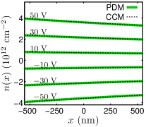
In the previous example, we have demonstrated that fabricating a series of patterned topgates may generate a periodic potential, which, combined with a potential linear in position as well as the periodically alternating mass potential, forms the prerequisite of the Bloch-Zener oscillation in graphene Krueckl2012 . In this demonstrating example, we point out a simple way to generate the linear potential: using a tilted backgate. As sketched in Fig. 7, where we consider a position-varying thickness of SiO2 with a slope of (an increase of per micron). In this case the quantum correction does not play a role (see Sec. 3.3.2), and we show in Fig. 7 only the carrier densities from the CCM and the PDM, which coincide to each other.
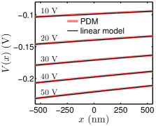
Since the classical capacitance model works well here, with the oxide thickness , where is the thickness at the center, we can describe the carrier density as and hence the potential as . The slope of the potential at , , together with the intercept , allows us to approximate the potential with a linear model,
| (29) |
In Fig. 7, we plot the potential profiles obtained from and from the linear model given by Eq. (29); the consistency is almost perfect.

4.5 Contact-induced doping and screening potential
In the last application example, we turn to a practical issue for the graphene electronics: contact-induced doping and its screening potential Khomyakov2009 ; Khomyakov2010 . Taking palladium as the specific example, we show that the solutions for the electric potential in graphene induced by the Pd contact solved by the PDM and by the QCM not only agree with each other but also are consistent with the previously reported results based on first principles Khomyakov2009 ; Khomyakov2010 , which we first briefly review as follows.
Previous first-principles study expected ideal Pd(111) contacts to dope graphene as n-type, with the shift of the Fermi level given by , where is the work function of the metal coated with graphene, and is the work function of free-standing graphene Khomyakov2009 . In the case of Pd, , so leads to , according to the table summarized in Khomyakov2009 . This means that the Fermi level of graphene coated by Pd(111) is expected to be . Furthermore, the contact-induced screening potential in graphene was calculated in Khomyakov2010 using the density functional theory within the Thomas-Fermi approximation, which is similar to the PDM introduced here since the underlying equation that governs the electrostatic potential is still the Poisson equation. In their formulation, the metal contact is oriented at (graphene sheet also at , and the boundary condition for the surface () of the contact is given by , where is the work function of the corresponding clean metal. In the case of Pd and again according to the table summarized in Khomyakov2009 , , leading to .
The numerically exact solution for the electric potential in graphene, i.e., for , was further fitted by a variational solution Khomyakov2010
| (30) |
with fitting parameters and . The scaling length in Eq. (30) is defined as with , where is assumed.101010In Khomyakov2010 , is given by possibly because of the slightly different Fermi velocity . For Pd, from their table (with ) one finds . Thus for vacuum with , we have . We will compare with this variational solution (30).
To apply the presently reviewed PDM and QCM to resolve the graphene electric potential , while keeping the results of Khomyakov2009 ; Khomyakov2010 unchanged, namely,
-
(i)
-
(ii)
decays nonlinearly with
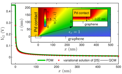
we may model the metal contact as a slightly floating gate located at , as schematically shown in the inset of Fig. 8. By such modeling, both of the above stated conclusions (i) and (ii) can be satisfied at one time by taking the same input of the boundary condition. Specifically, the boundary conditions to be applied here are , with the same according to Khomyakov2010 .
To satisfy (i), we may apply the QCM for the parallel-plate capacitor to deduce a proper floating height in order to meet the proper shift of the Fermi level . Thus the upper plate of the capacitor is the Pd contact with voltage , while the lower plate is graphene with voltage . Equation (24) therefore reads
| (31) |
where , with the classical capacitance of the contact-vacuum-graphene sandwich, has been substituted. Thus using in Eq. (31), one may solve for to obtain
| (32) |
For the present case of Pd and following of Khomyakov2009 and of Khomyakov2010 , this effective height given by Eq. (32) amounts to .
Setting for the contact and treating it as a “gate” with fixed potential , the electric potential in the graphene sheet is calculated by using the self-consistent PDM and the analytical QCM, as shown in Fig. 8. The two approaches again coincide with each other. In addition, is clearly observed, while the nonlinearly decaying agrees well with the variational solution of Khomyakov2010 , thus satisfying both (i) and (ii).
Note that despite the consistency with the previous theory shown here, experiments for transport measurements usually do not have single-crystal contacts grown along (111), and the contact/graphene interface is certainly dirty. The charge transfer between the metal contact and graphene due to their different work functions is, therefore, greatly reduced, leading to a much lower . For example, a recent experiment observing the ballistic interferences in ultra-clean suspended graphene uses Pd as contacts, and theoretical modeling with of the order of is found to better fit the transport measurement Rickhaus2013 .
5 Summary
In conclusion, theories of the gate-induced carrier density modulation in bulk graphene have been reviewed. The classical capacitance model, the widely adopted tool for carrier density estimation, does not include the quantum correction but nevertheless plays usually the dominant role in the gate modulation, unless the metal is rather close to graphene (Fig. 2). The quantum correction stems from the finite capacity of the graphene sheet for the electrons to reside, and can be treated by the self-consistent Poisson-Dirac iteration method, as well as the exactly solvable quantum capacitance model. By inspecting the numerical examples of single-gated graphene, these two approaches are shown to agree with each other. In particular, the correspondence is exact for the case of infinite parallel-plate capacitors (Fig. 3). For the case with finite gates, the agreement between QCM and PDM remains good (Fig. 4), implying that Eq. (27) is a good approximation for numerically calculating the spatially varying capacitance. This further suggests that the classical solution serves as the preliminary solution step for the exactly solvable QCM, circumventing the self-consistent iteration during the solution process that is needed in the PDM. Along with the brief introduction to the usage of the Matlab pdetool, the former part of this work (Secs. 2–3) provides a self-contained instruction to calculating the carrier density of pristine graphene sheets subject to complicated gating geometry. For the generalized theory for multigated doped graphene, the readers are referred to Liu2013 .
To demonstrate the applicability of the introduced CCM, PDM, and QCM, the latter part of this work (Sec. 4) is devoted to illustration of practical examples for calculating gate-induced carrier density in graphene sheets, including the graphene pnp junction using an embedded local gate in addition to a global backgate (Fig. 5), graphene superlattice potential by a series of patterned topgates (Fig. 6), quasi-linear potential by using a tilted backgate (Fig. 7), and finally the contact-induced doping and screening potential (Fig. 8). The first three examples correspond to the experimental conditions that provide a flexible platform to test the physics of Klein backscattering Shytov2008 ; Young2009 ; Nam2011 ; Liu2012a and the Bloch-Zener oscillation Krueckl2012 in graphene, while the last example shows that the effects of metal contacts can be treated equally well by the PDM and QCM, as compared to the previous first-principles studies Khomyakov2009 ; Khomyakov2010 . In either case, once the realistic potential profile is obtained, satisfactory electronic transport calculation for the relevant structure following Liu2012a can then be guaranteed.
Acknowledgements.
The author thanks T. Fang and D. Jena for their illuminating suggestions, F.-X. Schrettenbrunner, J. Eroms, P. Rickhaus, and R. Maurand for sharing their experimental viewpoints, and V. Krueckl and K. Richter for valuable discussions. Financial supports from Alexander von Humboldt Foundation (former part of the work) and Deutsche Forschungsgemeinschaft within SFB 689 (present) are gratefully acknowledged.References
- (1) A. H. Castro Neto, F. Guinea, N. M. R. Peres, K. S. Novoselov, and A. K. Geim, “The electronic properties of graphene,” Rev. Mod. Phys., vol. 81, p. 109, 2009.
- (2) S. Das Sarma, S. Adam, E. H. Hwang, and E. Rossi, “Electronic transport in two-dimensional graphene,” Rev. Mod. Phys., vol. 83, pp. 407–470, May 2011. [Online]. Available: http://link.aps.org/doi/10.1103/RevModPhys.83.407
- (3) K. S. Novoselov, A. K. Geim, S. V. Morozov, D. Jiang, Y. Zhang, S. V. Dubonos, I. V. Grigorieva, and A. A. Firsov, “Electric field effect in atomically thin carbon films,” Science, vol. 306, no. 5696, pp. 666–669, 2004.
- (4) B. Huard, J. A. Sulpizio, N. Stander, K. Todd, B. Yang, and D. Goldhaber-Gordon, “Transport measurements across a tunable potential barrier in graphene,” Phys. Rev. Lett., vol. 98, p. 236803, Jun 2007. [Online]. Available: http://link.aps.org/doi/10.1103/PhysRevLett.98.236803
- (5) J. R. Williams, L. DiCarlo, and C. M. Marcus, “Quantum hall effect in a gate-controlled p-n junction of graphene,” Science, vol. 317, no. 5838, pp. 638–641, 2007. [Online]. Available: http://www.sciencemag.org/content/317/5838/638.abstract
- (6) B. Özyilmaz, P. Jarillo-Herrero, D. Efetov, D. A. Abanin, L. S. Levitov, and P. Kim, “Electronic transport and quantum hall effect in bipolar graphene junctions,” Phys. Rev. Lett., vol. 99, p. 166804, Oct 2007. [Online]. Available: http://link.aps.org/doi/10.1103/PhysRevLett.99.166804
- (7) G. Liu, J. J. Velasco, W. Bao, and C. N. Lau, “Fabrication of graphene p-n-p junctions with contactless top gates,” Appl. Phys. Lett., vol. 92, no. 20, p. 203103, 2008. [Online]. Available: http://dx.doi.org/doi/10.1063/1.2928234
- (8) R. V. Gorbachev, A. S. Mayorov, A. K. Savchenko, D. W. Horsell, and F. Guinea, “Conductance of p-n-p graphene structures with “air-bridge” top gates,” Nano Letters, vol. 8, no. 7, pp. 1995–1999, 2008. [Online]. Available: http://pubs.acs.org/doi/abs/10.1021/nl801059v
- (9) V. V. Cheianov and V. I. Fal’ko, “Selective transmission of Dirac electrons and ballistic magnetoresistance of n-p junctions in graphene,” Phys. Rev. B, vol. 74, no. 4, p. 041403, JUL 2006.
- (10) M. I. Katsnelson, K. S. Novoselov, and A. K. Geim, “Chiral tunnelling and the klein paradox in graphene,” Nat. Phys., vol. 2, no. 9, p. 620, SEP 2006.
- (11) N. Stander, B. Huard, and D. Goldhaber-Gordon, “Evidence for klein tunneling in graphene junctions,” Phys. Rev. Lett., vol. 102, p. 026807, Jan 2009. [Online]. Available: http://link.aps.org/doi/10.1103/PhysRevLett.102.026807
- (12) A. F. Young and P. Kim, “Quantum interference and klein tunnelling in graphene heterojunctions,” Nat. Phys., vol. 5, no. 3, pp. 222–226, MAR 2009.
- (13) S.-G. Nam, D.-K. Ki, J. W. Park, Y. Kim, J. S. Kim, and H.-J. Lee, “Ballistic transport of graphene pnp junctions with embedded local gates,” Nanotechnology, vol. 22, no. 41, p. 415203, 2011.
- (14) J. Guo, Y. Yoon, and Y. Ouyang, “Gate electrostatics and quantum capacitance of graphene nanoribbons,” Nano Letters, vol. 7, no. 7, pp. 1935–1940, 2007. [Online]. Available: http://pubs.acs.org/doi/abs/10.1021/nl0706190
- (15) J. Fernández-Rossier, J. J. Palacios, and L. Brey, “Electronic structure of gated graphene and graphene ribbons,” Phys. Rev. B, vol. 75, p. 205441, May 2007. [Online]. Available: http://link.aps.org/doi/10.1103/PhysRevB.75.205441
- (16) T. Fang, A. Konar, H. Xing, and D. Jena, “Carrier statistics and quantum capacitance of graphene sheets and ribbons,” Appl. Phys. Lett., vol. 91, no. 9, p. 092109, 2007. [Online]. Available: http://link.aip.org/link/?APL/91/092109/1
- (17) A. A. Shylau, J. W. Kłos, and I. V. Zozoulenko, “Capacitance of graphene nanoribbons,” Phys. Rev. B, vol. 80, p. 205402, Nov 2009. [Online]. Available: http://link.aps.org/doi/10.1103/PhysRevB.80.205402
- (18) T. Andrijauskas, A. A. Shylau, and I. V. Zozoulenko, “Thomas-fermi and poisson modeling of gate electrostatics in graphene nanoribbon,” Lithuanian Journal of Physics, vol. 52, no. 1, pp. 63–69, 2012.
- (19) S. Luryi, “Quantum capacitance devices,” Appl. Phys. Lett., vol. 52, no. 6, pp. 501–503, 1988. [Online]. Available: http://link.aip.org/link/?APL/52/501/1
- (20) M.-H. Liu, “Theory of carrier density in multigated doped graphene sheets with quantum correction,” Phys. Rev. B, vol. 87, p. 125427, Mar 2013. [Online]. Available: http://link.aps.org/doi/10.1103/PhysRevB.87.125427
- (21) M.-H. Liu and K. Richter, “Efficient quantum transport simulation for bulk graphene heterojunctions,” Phys. Rev. B, vol. 86, p. 115455, Sep 2012. [Online]. Available: http://link.aps.org/doi/10.1103/PhysRevB.86.115455
- (22) A. V. Shytov, M. S. Rudner, and L. S. Levitov, “Klein backscattering and fabry-pérot interference in graphene heterojunctions,” Phys. Rev. Lett., vol. 101, p. 156804, Oct 2008. [Online]. Available: http://link.aps.org/doi/10.1103/PhysRevLett.101.156804
- (23) V. Krueckl and K. Richter, “Bloch-zener oscillations in graphene and topological insulators,” Phys. Rev. B, vol. 85, p. 115433, Mar 2012. [Online]. Available: http://link.aps.org/doi/10.1103/PhysRevB.85.115433
- (24) P. A. Khomyakov, G. Giovannetti, P. C. Rusu, G. Brocks, J. van den Brink, and P. J. Kelly, “First-principles study of the interaction and charge transfer between graphene and metals,” Phys. Rev. B, vol. 79, p. 195425, May 2009. [Online]. Available: http://link.aps.org/doi/10.1103/PhysRevB.79.195425
- (25) P. A. Khomyakov, A. A. Starikov, G. Brocks, and P. J. Kelly, “Nonlinear screening of charges induced in graphene by metal contacts,” Phys. Rev. B, vol. 82, p. 115437, Sep 2010. [Online]. Available: http://link.aps.org/doi/10.1103/PhysRevB.82.115437
- (26) Partial Differential Equation ToolboxTM User’s Guide, Matlab 2012a ed., The MathWorks, Inc., 2012.
- (27) E. I. Rashba, “Properties of semiconductors with an extremum loop i. cyclotron and combinational resonance in a magnetic field perpendicular to the plane of the loop,” Sov. Phys. Solid State, vol. 2, p. 1109, 1960.
- (28) Y. A. Bychkov and E. I. Rashba, “Properties of a 2d electron-gas with lifted spectral degeneracy,” JETP Lett., vol. 39, p. 78, 1984.
- (29) M. Gmitra, S. Konschuh, C. Ertler, C. Ambrosch-Draxl, and J. Fabian, “Band-structure topologies of graphene: Spin-orbit coupling effects from first principles,” Phys. Rev. B, vol. 80, p. 235431, Dec 2009. [Online]. Available: http://link.aps.org/doi/10.1103/PhysRevB.80.235431
- (30) S. Abdelouahed, A. Ernst, J. Henk, I. V. Maznichenko, and I. Mertig, “Spin-split electronic states in graphene: Effects due to lattice deformation, rashba effect, and adatoms by first principles,” Phys. Rev. B, vol. 82, p. 125424, Sep 2010. [Online]. Available: http://link.aps.org/doi/10.1103/PhysRevB.82.125424
- (31) A. Yamakage, K.-I. Imura, J. Cayssol, and Y. Kuramoto, “Interfacial charge and spin transport in topological insulators,” Phys. Rev. B, vol. 83, p. 125401, Mar 2011. [Online]. Available: http://link.aps.org/doi/10.1103/PhysRevB.83.125401
- (32) H. Y. Tian, Y. H. Yang, and J. Wang, “Interfacial charge current in a magnetised/normal graphene junction,” EUROPEAN PHYSICAL JOURNAL B, vol. 85, no. 8, AUG 2012.
- (33) A. Yamakage, K. I. Imura, J. Cayssol, and Y. Kuramoto, “Spin-orbit effects in a graphene bipolar pn junction,” EPL, vol. 87, no. 4, AUG 2009.
- (34) M.-H. Liu, J. Bundesmann, and K. Richter, “Spin-dependent klein tunneling in graphene: Role of rashba spin-orbit coupling,” Phys. Rev. B, vol. 85, p. 085406, Feb 2012. [Online]. Available: http://link.aps.org/doi/10.1103/PhysRevB.85.085406
- (35) M. Rataj and J. Barnaś, “Graphene p-n junctions with nonuniform rashba spin-orbit coupling,” Appl. Phys. Lett., vol. 99, no. 16, p. 162107, 2011. [Online]. Available: http://dx.doi.org/10.1063/1.3641873
- (36) J. Sánchez-Barriga, A. Varykhalov, M. R. Scholz, O. Rader, D. Marchenko, A. Rybkin, A. M. Shikin, and E. Vescovo, “Chemical vapour deposition of graphene on Ni(111) and Co(0001) and intercalation with Au to study Dirac-cone formation and Rashba splitting,” Diamond and Related Materials, vol. 19, no. 7-9, SI, pp. 734–741, JUL-SEP 2010, 20th European Conference on Diamond, Diamond-Like Materials, Carbon Nanotubes and Nitrides, Athens, GREECE, SEP 06-10, 2009.
- (37) J. Xia, F. Chen, J. Li, and N. Tao, “Measurement of the quantum capacitance of graphene,” Nature Nanotechnology, vol. 4, no. 8, pp. 505–509, AUG 2009.
- (38) S. Dröscher, P. Roulleau, F. Molitor, P. Studerus, C. Stampfer, K. Ensslin, and T. Ihn, “Quantum capacitance and density of states of graphene,” Applied Physics Letters, vol. 96, no. 15, p. 152104, 2010. [Online]. Available: http://link.aip.org/link/?APL/96/152104/1
- (39) L. A. Ponomarenko, R. Yang, R. V. Gorbachev, P. Blake, A. S. Mayorov, K. S. Novoselov, M. I. Katsnelson, and A. K. Geim, “Density of states and zero landau level probed through capacitance of graphene,” Phys. Rev. Lett., vol. 105, p. 136801, Sep 2010. [Online]. Available: http://link.aps.org/doi/10.1103/PhysRevLett.105.136801
- (40) J. Martin, N. Akerman, G. Ulbricht, T. Lohmann, J. H. Smet, K. Von Klitzing, and A. Yacoby, “Observation of electron-hole puddles in graphene using a scanning single-electron transistor,” Nat. Phys., vol. 4, no. 2, pp. 144–148, FEB 2008.
- (41) H. Xu, Z. Zhang, and L.-M. Peng, “Measurements and microscopic model of quantum capacitance in graphene,” Applied Physics Letters, vol. 98, no. 13, p. 133122, 2011. [Online]. Available: http://link.aip.org/link/?APL/98/133122/1
- (42) P. Rickhaus, R. Maurand, M.-H. Liu, M. Weiss, K. Richter, and C. Schönenberger, “Ballistic interferences in suspended graphene,” March 2013, unpublished.