Electronic transport in two dimensional Si:P -doped layers
Abstract
We investigate theoretically 2D electronic transport in Si:P -doped layers limited by charged-dopant scattering. Since the carrier density is approximately equal to the dopant impurity density, the density dependent transport shows qualitatively different behavior from that of the well-studied 2D Si-MOSFETs where the carrier density is independent of the impurity density. We find that the density dependent mobility of the Si:P system shows non-monotonic behavior which is exactly opposite of the non-monotonicity observed in Si-MOSFETs — in the Si:P system the mobility first decreases with increasing density and then it increases slowly with increasing density above a typical density cm-2 (in contrast to Si MOSFETs where the mobility typically increases with density first and then slowly decreases at high density as surface roughness scattering dominates). In the low density limit (or strong screening limit) mobility decreases inversely with increasing density, but in the high density limit (or weak screening limit) it slowly increases due to the finite width effects of the 2D layer. In the intermediate density regime (, where , , and are the confinement width of the -layer, Fermi wave vector, and Thomas-Fermi screening wave vector, respectively) the density dependent mobility is approximately a constant at the minimum value. However, the calculated mean free path increase monotonically with density. We also compare the transport scattering time relevant to the mobility and the single particle relaxation time relevant the quantum level broadening, finding that the transport scattering time could be much larger than the single-particle scattering time unlike in Si MOSFETs where they are approximately equal.
I introduction
In semiconductor based quantum computers, where electron spin (or charge) localized at dopant sites could be used as qubitskane1998 , it is extremely important to very precisely place dopants with atomic precision within the host latticekoiller2001 . This has motivated a materials science initiative to create precisely located dopant structures within semiconductor hosts, e.g. P in Si or Ge. In particular, the scanning tunneling microscopy (STM) based lithographylyding1994 has been used to position dopants with atomic scale precision schofield2003 within semiconductors. The ability of controlling the location of individual dopant atoms within a semiconductor provides future potential towards atomic scale deviceskane1998 ; koiller2001 ; snider1999 . Recently, Si:P -doped two dimensional (2D) structures in silicon have attracted interest with their potential applications in multiqubit quantum computer architectureskoiller2001 and atomic-scale device shen2004 ; ruess2005 ; wilson2004 ; zudov2003 ; goh2006 . The effect of doping density on electronic transport in Si:P -doped layers grown by phosphine dosing and low temperature molecular beam epitaxy have been investigated in experimentsshen2004 ; ruess2005 ; wilson2004 ; zudov2003 ; goh2006 ; weber2012 . Unlike other 2D systems, the carrier concentration in this -doped layers can reach cm-2 or higher, which exceeds a typical carrier density found in GaAs-based systems or Si-MOSFETs by more than two orders of magnitude.
Even though the carrier density of Si:P -doped layers is extremely high the measured mobilitieszudov2003 ; goh2006 ; weber2012 ; fuechsle2010 at are very low cm2/Vs in P doping levels of cm-2. Thus, in these layers the mean free path is of the order of only a few nm and the corresponding transport relaxation time is in the femtosecond range. In addition, as the carrier density increases mobility decreases at first, but the mean free path increases linearly. These behaviors are opposite to those found in extensively studied 2D Si MOSFET and GaAs/AlGaAs systems. It is, of course, expected that the electronic transport mobility of the Si:P -doped systems is lower than that in modulation-doped GaAs systems because the charged dopant impurities in Si:P layers are located inside the layer, but the mobility for the Si:P system is substantially lower than Si MOSFET mobility also. However, the density dependence of low-temperature transport in Si:P layers is unusual because it is dominated entirely by the dopant charged Coulomb impurity scattering ando1982 ; dassarma2011 . The mobility increases with increasing density when the charged impurity scattering dominates in the high density regime. In Si-MOSFETs, due to the surface roughness scattering at high densities, the mobility decreases with increasing carrier density in the high density regime dominated by surface roughness scattering which however plays no role in the transport properties of Si:P delta-layers since the carriers are located away from the surface inside the semiconductor. It is also reported that in Si:P -doped samples with the doping density of cm-2 a non-Ohmic behavior is observed, suggesting that a transition to Anderson localization for Si:P -doped layers occurs below cm-2. The similar low-density localization behavior is also observed in other -doped samples like Si:Sb and Si:B -doped layers agan2001 .
These experimental features of -doped layers provide a unique opportunity to study the carrier density dependent transport of ultrahigh density 2D systems limited by only charged Coulomb disorder. Since the carriers remain confined to a dopant plane by strong-confining electrical fields, charged Coulomb scattering by the ionized dopants themselves significantly limits the mobility. In spite of there being very interesting experimental studies in the ultrahigh density -doped systems, the systematic theoretical investigation of transport properties has not yet been carried out. The purpose of this paper is to theoretically study the transport properties of Si:P -doped layers. It is obviously important to understand the detailed transport properties for eventual applications to atomic-scale devices and semiconductor multiqubit architectures.
In addition to atomic scale device application motivation there are several fundamental reasons which make transport studies of 2D -doped structures interesting and important in its own right. First, these systems allow the study of 2D carrier transport properties at unprecedented high carrier densities of cm-2 or above, which is much higher than the typical cm-2 density regime studied extensively in the context of GaAs heterostructures and Si MOSFETs. Second, these systems allow for studying carrier transport limited almost entirely by long-range Coulomb disorder (arising from the ionized dopants producing the carriers in the system) without complications from other mechanisms often operational in 2D semiconductor systems such as surface roughness scattering and alloy disorder scattering. Third, the -doped 2D systems enable the study of carrier transport in the scattering regime where the carrier density is roughly equal to (or perhaps even somewhat less than) the impurity density since each electron must leave behind an ionized impurity. Fourth, by changing carrier density, one could study the strong screening to the weak screening 2D transport regime, which is not possible in other 2D systems. All of these features are unique to the -doped 2D systems making them complementary to the traditional 2D semiconductor systems and thus providing particular fundamental impetus to our work. We mention that 2D electron systems possess the highly peculiar behavior, arising from the constant 2D density of states which is energy independent. The low-carrier density regime is the strong-screening regime (where ) and the high-density regime is the weak-screening regime (where ), and therefore, the ability to go to very high carrier density provides a completely new perspective in the study of 2D semiconductor systems, which is not available in the well-known Si MOSFET and GaAs heterostructure based 2D systems.
In this paper we investigate the low-temperature electronic transport in Si:P -doped ultra-high density 2D electron systems. Employing Boltzmann transport theory, we calculate density dependent mobility and scattering times of Si:P -doped layers in a variety of experimental situations. The electrons in realistic -doped systems, where there are likely sources of additional scattering arising from unintentional background impurities, may localize at low densities (), but in this paper we neglect localization effects and show our calculated results in the wide range of density cm-2. In fact, our theoretical results based on the semiclassical Boltzmann theory give a clue about the density range of strong localization in the system, which we discuss later in the paper. All our explicit results (as presented in our figures) for mobility, mean free path, and scattering time explicitly assume that the 2D carrier density is precisely equal to the 2D quenched charged impurity density, and therefore, our mobility results are an upper bound to the experimental mobility since the real systems studied in the laboratory are likely to have additional impurities not related to the dopants used in creating the electron gas. We expect the measured mobility and conductivity to be somewhat smaller than that calculated by us, but we expect the experimental mobility to approach our theoretically calculated results with improvement in the sample quality. The calculation within the density functional theory shows that the band structure of a Si:P -doped layer is a symmetric V-shaped potential well drumm2012 ; budi2012 ; lee2011 ; qian2005 ; carter2009 , but we use the square well model with a width as a -doped 2D layer. We confirm that our calculated results are not sensitive to the shape of the confinement potential by also doing a calculation using a triangular confinement potential. The calculated transport results depend only on the characteristic confinement length ’’ defining the thickness of the 2D electron layer, and not on the details of the confining wavefunction itself.
The rest of this paper is organized as follows: in section II we provide the detailed transport theory and the analytic results for both high and low densities, and in section III we show the numerical results of mobility and scattering times of Si:P -doped layers. We conclude in section IV with a discussion.
II theory
The Si:P -doped layer is a conducting layer of atomic thickness, which is formed in a pure semiconducting crystal matrix due to dopant atoms located within one crystallographic plane. The electrons in the potential well form a 2D electron gas in the plane of the layer, and behave as 2D free carriers with appropriate effective mass and spin/valley degeneracy quantum mechanically confined by the ionized dopant-induced electric field within a quasi-2D layer of thickness ’’. The electrons in a Si:P -doped layer are spatially confined along the normal direction with respect to the layer of P dopants. In this paper we designate the 2D layer as plane and the normal direction of the layer as the direction ( being the center of the well). The wave function of an electron in the layer is given by
| (1) |
where is the confinement wave function in -direction, is the 2D electron wave vector in the plane, and . The calculated band structure of Si:P -doped layer depends sensitively on the disorder model (i.e., the nature of symmetry, the exact placement of dopants, other unknown fixed charges in the system, and the size of the unit cell, etc.). However, for simplicity, we assume that the confinement profile is described by a square quantum well structure. Although the quantum well may be a simplification of the actual situation drumm2012 ; budi2012 ; lee2011 , our calculated results describe quantitatively the transport properties of the Si:P -doped layer since the details of the confinement are not quantitatively important except for the confinement width, which we parametrize.
To calculate the 2D mobility of Si:P -doped layers, we use the Drude-Boltzmann semiclassical theory for 2D transport limited by the scattering from charged impurities (i.e., dopants) ando1982 ; dassarma2011 . We assume that the impurities (P dopants) are randomly distributed in the x-y plane at , i.e., the center of the quantum well and the 2D carrier conductivity is entirely limited by charged impurity scattering. Since the Fermi temperature is very high ( K) at the density cm-2 and the Bloch-Grüneisen temperature at this density is very high we neglect phonon scattering in this calculation. The Bloch-Grüneisen temperature at the electron density cm-2 becomes K with the phonon velocity of Si cm/s. Below acoustic phonons cease to be appreciably excited, and no longer contribute to the relaxation rate kawamura1992 . We therefore include scattering by the random quenched charged dopants as the only resistive mechanism in our theory.
By considering the charged impurity centers located at with an impurity density and taking k and to denote the 2D electron wave vector before and after scattering, respectively, by a Coulomb scatterer (i.e., P dopant) we have the transport scattering time in the Born approximation
| (2) |
where is the screened Coulomb potential for electron-charged impurity interaction, is the momentum transfer, is the scattering angle, and is the electron energy.
The unscreened potential of a charged center located at is given by , where is the background dielectric function of Si. The 2D Fourier transform of becomes , where is the 2D bare Coulomb interaction and is the form factor of electron-impurity interaction and given by
| (3) |
The form factor becomes unity in the limit of vanishing . The screening effect can be included by dividing by the RPA dielectric screening function, , due to the 2D electrons themselves,
| (4) |
where is the 2D bare Coulomb interaction, is the form factor for electron-electron interaction, and is the 2D finite wave vector polarizability function ando1982 ; dassarma2011 . Thus, the screened Coulomb potential for electron-charged impurity interaction becomes . The form factor for electron-electron interaction associated with the confinement wave function is defined by
| (5) |
where is a confining wave function in the direction. When the -doped impurities are located at from the center of the confinement potential the electron-impurity Coulomb interaction has the factor and becomes .
If we take the confining potential in the direction to be of square-well form, then the quantized ground state wave function is given by for and for with denoting the width of the square well. In this case the form factors and are calculated as
| (6) |
and
| (7) |
As a result of the external dc electric field (E) driving the electric current in the system the Fermi distribution function is deformed from equilibrium distribution where is the inverse temperature and is the chemical potential, i.e., where is proportional to the applied electric field. In the relaxation time approximation ando1982 , where is the carrier velocity. Thus, an induced current density due to the electric field in a -layer is given by
| (8) |
where is the total degeneracy including the usual spin degeneracy of two plus any possible valley degeneracy arising from the bulk band structure of the system. From the definition of the drift mobility and the conductivity , we have and , where is the carrier effective mass and the energy averaged transport relaxation time is given by
| (9) |
where is the density of states with total degeneracy , is the 2D electron energy dispersion, and is the energy dependent transport relaxation time given in Eq. (2).
Since we are interested in the low-temperature density dependent transport () of Si:P -doped layers we first consider the zero temperature limit. After performing the integration in Eq. (2) and taking (i.e. the Fermi wave vector) we have
| (10) |
where ( is a 2D Thomas-Fermi wave vector with effective Bohr radius ),
| (11) |
and
| (12) |
Due to the form factors it is not possible to get the full analytic formula for Eq. (12). However, we can get asymptotic forms of Eq. (12) for different density regions where large or small approximation may apply. For Si(100) we have Å for electrons in the conduction band and , where . Thus, in the low density limit () (i.e., strong screening limit), and if (i.e. ), then the form factors are close to unity and is given by
| (13) |
Now the scattering time becomes , which is independent of carrier density . However in Si:P -doped layer the dopant density is equal to the carrier density because every P atom gives up one free electron to the layer (as stated above, in real samples it is more likely that since there could be background unintentional impurities in the system, but provides a lower bound for the impurity density). Thus, the scattering time and the density dependent mobility is inversely proportional to the density, , in the strong screening limit ().
In the high density limit ( cm-2 which is the relevant density range in the currently available Si:P -doped layers) (i.e. weak screening limit) we can approximately express Eq. (12) as
| (14) |
Then, we have
| (15) | |||||
Thus for we have , and mobility . For the mobility is independent of carrier density. For we have , and the mobility becomes . For the mobility increases as as the carrier density increases.
Combining all the results we have so far we can conclude that as the carrier density (or doping density) increases the mobility decreases as up to . As the carrier density increases further beyond this point the density dependent mobility saturates up to , and then it increases as when . Thus the mobility behavior in the delta-doped layers as a function of carrier density (or dopant density since we assume them to be the same in our model) has three distinct regimes: a low-density strong-screening regime where the mobility decreases (as ) with increasing density, an intermediate-density saturation regime where the mobility is approximately a constant in density, and then a high-density weak-screening regime where the mobility rises with density (as ). This behavior, which is clearly manifested in our full numerical results shown in the next section, is in sharp contrast with 2D transport in Si MOSFETs where the mobility first increases with carrier density as Coulomb disorder gets screened out and then decreases with carrier density as surface roughness scattering becomes dominant. We note that if the system is strictly two-dimensional (i.e. the electrons are confined in an infinitesimally thin 2D layer), then the form-factors in Eq. (12) both become unity, and the mobility will decrease monotonically with increasing carrier density finally saturating at high enough density where condition is satisfied. The third regime of an eventual increase of mobility at high density arises entirely from the quasi-2D form factor effect which becomes crucial at very high density when , which would not apply if , i.e. in the strict 2D limit. We emphasize again that our theory is an upper bound to the expected experimental mobility since we are only including scattering by the charged dopants themselves ignoring all other possible scattering sources.
III results
In this calculation we use the following parameters; for Si(100) surface orientation the effective mass and valley degeneracy , and for Si(110) surface orientation and . We use the spin-degeneracy everywhere. We set the carrier density to be equal to the dopant impurity density, i.e., . We also take a square quantum well with width as a confinement potential. (We have explicitly verified that our numerical results change little for a triangular potential well as long as the same effective quasi-2D confinement width is used in the theory.) We also mention that mobility is simply related to the conductivity by the formula .
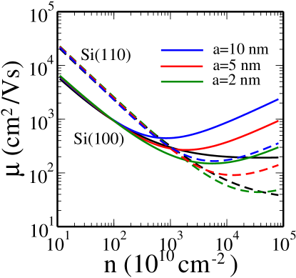
In Fig. 1 we show the calculated mobility of Si:P -doped layers as a function of density for different quantum well width , 5, and 10 nm. For comparison we also show the results (black lines) calculated with Howard-Fang (HF) variational wave functionando1982 . In Fig. 1 charged impurities (dopants) are located at (i.e. the center of quantum well). In the low density limit (or strong screening limit, ) the calculated mobility is inversely proportional to the density () as the density increases upto . In this limit the effect of the finite 2D layer width is small since is small and the form factors are effectively unity. Note that for Si(100) surface orientation Å-1, which gives cm-2. For Si(110) surface orientation Å-1 and cm-2. When the density increases further, , mobility has a minimum value at . In the weak screening high-density limit () the form factor of electron-impurity interaction arising from the finite width of the 2D layer affects the density dependent mobility since now and the form factors become relevant. For both and the mobility increases as . In Fig. 1 the non-monotonic density dependent mobility as a function of density is shown, i.e., as the carrier density increases mobility decreases first, reached a minimum, and then it increases again. Thus, the three density regimes (low, intermediate, and high) discussed analytically in the last section are clearly apparent in Fig. 1 with mobility decreasing first with increasing density, then saturating around a minimum value around an intermediate density before increasing again at higher density. The characteristic intermediate density for the mobility minimum increases as the quantum well width decreases. Fig. 1 also shows the degeneracy dependent mobility. At low densities cm-2 the mobility of Si(110), which has a higher degeneracy factor and hence stronger screening, is higher than that of Si(100), but at high densities the mobility of Si(100) is higher. We can understand this degeneracy dependence from the scattering time. From Eq. (10) we findhwang2012 for (strong screening limit) and for (weak screening limit).
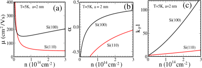
In order to clearly see the high density behavior of mobility we show in Fig. 2(a) the calculated mobility in linear scale as a function of density at a finite temperature . The black (red) lines represent the mobility calculated with parameters of Si(100) [Si(110)]. The well width nm is used in this calculation and the impurities are located at . Fig. 2(b) shows the exponent of density dependent mobility for the results shown in (a), i.e. exponent in the relation of . As described in Sec. II the exponent of Si(100) samples eventually approaches as the carrier density increases. Fig. 2(c) shows the calculated as a function of density where the mean free path is defined by . Note that , where the conductivity has a unit and is the total degeneracy. In terms of mobility we can express it as , where is measured in units of cm and . The calculated increases super-linearly due to the finite width effect. In Sec. II we show that for and . Thus in this high density limit we expect that the mean free path increases linearly with density, , and this behavior is experimentally observed in Si:P -doped layers goh2006 . However, in the strict 2D limit increases linearly with density and . The linear increase of with arises from the finite width effect of the layer as discussed analytically in Sec. II.
So far we have only considered the transport scattering time () which is relevant to the conductivity or mobility as shown in Sec. II. In general, in the presence of disorder scattering there are two distinct relaxation timesdassarma1985 : the scattering lifetime or the transport relaxation time ( or ) and the quantum lifetime or the single particle relaxation time ( or ). These two characteristic times of the system differ by the important vertex correction factor. The relaxation rate is given by making the replacement in the integrand for the formula for in Eq. (2). In general, determines the quantum level broadening, , of the momentum eigenstates, and physically, it simply represents the time between scattering events between electron and impurity. Considering the difference between two scattering times we calculate the single particle relaxation time and compare it with the transport scattering time in following two figures. We mention that just as the transport scattering time determines the conductivity or the mobility of the system, the single particle relaxation time determines level broadening as measured in Shubnikov-de Haas (SdH) measurements — in fact, the Dingle temperature of SdH measurements is given by defined above using . In strong screening systems or for short-range disorder scattering (as in 3D metals or 2D Si MOSFETs), generally, and one does not need to discuss two distinct impurity scattering times. This is not true in Si:P -layers at high density where the system is weakly screened, and the two scattering times could differ by a very large factor in the presence of long-range Coulomb disorder.
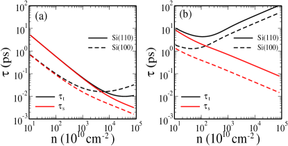
In Fig. 3(a) we show the transport scattering time, , and single particle relaxation time, , of Si:P -doped layers as a function of density for both Si(100) and Si(110). The charged impurities are located at (center of the well). The well width nm is used in this calculation. In Fig. 3(b) we show the scattering times assuming the impurities to be outside the quantum well, i.e. impurities at . By replacing with 1 in Eq. (2) we have for (strong screening limit or low density limit). In the opposite limit () we have , assuming . Thus, unlike , as the carrier density increases the calculated single particle relaxation time decreases continuously without any upturn which appears in the transport scattering time [see Fig. 3(a)]. When the charged impurities are located outside the quantum well (remote doping) the very strong enhancement in the transport scattering time is found since large-angle scattering ( scattering) by the remote impurities (which is most weighted in ) is strongly suppressed by the separation. The single particle relaxation time is also enhanced, but the enhancement is much smaller than that of since all angles contribute to [see Fig. 3(b)].
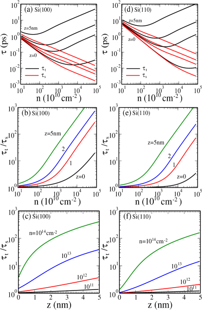
In Fig. 4 we show the calculated scattering times and the ration of to for both Si(100) and Si(110). As shown in Figs. 4(a) and (d) the transport scattering time, , shows nonmonotonic behavior and strongly depends on the location of dopant impurities. However, the single particle relaxation time, , decreases monotonically as the density increases, and has weaker dependence on impurity location. In the strong screening limit and we have and, therefore,. At high densities () and we have , but due to the factor arising from the separation between electrons and impurities the ratio is much enhanced as shown in Fig. 4.
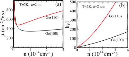
Finally, in Fig. 5(a) we show the calculated mobility in a Ge:P -doped layer as a function of density at a finite temperature, . Recently Ge:P -doped layers have also attracted a lot of interest due to the higher mobility in Ge than in Si scappucci2009 . In this calculation we use the following parameters: effective mass , background dielectric constant , and the valley degeneracy for Ge(100) surface and for Ge(110) surface. We use the well width nm and assume the dopants are located at . Fig. 5(b) shows as a function of density where the mean free path is given by . We find that the mobility in a Ge:P -doped layer is enhanced by a factor of 10 compared with the mobility in a Si:P -doped layer. However, the overall density dependent transport behavior of the Ge:P is very similar to that of Si:P. Due to the large value of the effective Bohr radius in Ge ( Å) the in Ge:P is much smaller than that of Si:P. Thus we find that after reaching a minimum point in the density dependent mobility the upturn density is much smaller in a Ge:P -doped layer than that in a Si:P -doped layer.
IV discussion and conclusion
Before concluding, we first want to discuss two issues not discussed in the earlier sections with respect to our results. These are the important questions of comparison between experiment and our theory and the issue of localization, which is of course experimentally relevant, but is not explicitly included in our semiclassical Boltzmann theory.
First, in comparing our theory qualitatively to experiment, we note that our theoretical results are at best an upper limit on the experimental mobility since we have assumed the ionized dopants to be the only source of resistive scattering whereas in reality there are likely to be other sources of disorder (e.g. unintentional and hence unknown impurities) in addition to the charged dopants. We therefore expect our results to agree with only the best available samples where other sources of scattering are presumably suppressed. This is indeed the case. The current highest measured mobility of Si:P (100) -layer comes from the Sandia National Labbussmann where the samples after annealing reached a mobility at 5K of close to 200 cm2/Vs at a carrier density of cm-2. According to our Fig. 1, the mobility for the Si:P (100) -layer varies between 200 and 500 cm2/Vs which is consistent with the experimental data (and is in fact in agreement with it if we use the lower value of the 2D confinement width). All other existing experimental mobility data in the literature fall below our calculated value (but none above) because the currently existing samples are not yet optimized and still presumably contain substantial amount of unintentional quenched impurities. This conclusion is consistent with the Sandia finding that the mobility increased substantially (by more than a factor of 2) upon annealing which presumably got rid of some of the unintentional impurities in the system. In any case, our results presented in this paper should motivate the experimentalists in producing density dependent mobility data in Si and Ge -doped 2D systems so that a careful quantitative comparison can be carried out, which is not possible at this stage because of the dearth of detailed experimental data.
Second, we can discuss the onset of strong localization within our Boltzmann theory by asking where the Ioffe-Reggel-Mott criterionlee1985 for strong localization, , starts to get satisfied in our system. This will again provide us with an intrinsic limit on localization since we assume which would underestimate the actual localization density in real samples where is the likely situation because of unintentional impurities. We note that our calculated [Fig. 2(c)] increases monotonically with density, and thus the localization condition of is a low-density condition, which is consistent with experimental data where the localization behavior is seen only for cm-2. In fact, for cm-2, we get in Si:P (100) 2D system, which is far from the strongly localized regime. Using our simple formula derived in Section III, we see from Fig. 1(a) that for cm-2 (where our calculated cm2/Vs), which is rather close to the strong localization condition. Therefore, it is indeed possible that the actual localization in realistic samples (where the mobility is likely to be lower than our calculated results assuming that the ionized dopants are the only scattering source) occurs around cm-2 carrier density.
We also comment on our finding of a mobility minimum at a characteristic density in the 2D -doped system. Since defines the crossover from the strong screening to the weak screening behavior in the system, we can crudely obtain from the condition , i.e. . This happens for Si(100) system at cm-2, which is roughly where the mobility starts to go from a decreasing function of density to an increasing function of density in Fig. 1. It will be very interesting to observe this strong to weak screening crossover directly experimentally.
In conclusion, we have studied the effect of doping density on electronic transport in 2D Si:P -doped layers. Since the carrier density is equal to the dopant impurity density we find that the density dependent transport is qualitatively different from that of Si-MOSFETs where the carrier density is independent of the impurity density since carriers are induced by a gate and the impurities are unintentional oxide charges at the interface. The density dependent mobility of a Si:P -doped layer is also different from that of a modulation -doped 2D GaAs quantum well system because of the physical separation between electrons and dopants in the GaAs system. We find that the density dependent mobility of the Si:P system shows a non-monotonic behavior. At the mobility has a minimum value. However, the calculated mean free path increases monotonically with increasing density as observed experimentally goh2006 . We also calculate both the transport scattering time and the single particle relaxation time in Si:P -doped layers. The shows nonmonotonic behavior like mobility and strongly depends on the location of impurities, but the keeps decreasing with increasing density and is less sensitive to the location of impurity.
In this paper we have simplified the confinement potential as a square quantum well and neglected two important features of high density Si:P samples; the localization effects and the multisubband effects. As shown in Fig. 1 our results are not sensitive to the shape of the confinement potential, and given that the exact impurity and dopant configurations in real samples are not known accurately, we do not see much point in trying to improve our confinement model. Since the localization effects are observed at very low densities ( cm-2) our results may not be applicable to the actual experiment in this density range. Usually in Si:P -doped layers only a few subbands are filled. Even though the mobility of carriers depends on the intersubband scattering ando1982 we expect that our results quantitatively explain the observed experimental data. In particular, as emphasized throughout this paper, our work provides the upper limit on the possible achievable mobility in delta-doped 2D systems since we include the only source of scattering that must always be present in the system, namely, the scattering by the ionized dopants contributing the electrons to the system. The experimental mobility can be lower than our calculated results, but it can never be higher. Our estimate of the localization density using the Ioffe-Regge-Mott criterion indicates that high-quality intrinsic delta-doped samples with very little unintentional background impurities may very well show effective metallic behavior at carrier density cm-2 or lower, but much of the strongly metallic behavior most likely manifests for density around cm-2 or higher. Our work should motivate detailed experimental transport studies for this interesting and novel class of 2D electron systems which allow the study of 2D transport at very high carrier density along with very high impurity density, a transport regime little studied before in 2D electron systems.
acknowledgments
This work was supported by LPS-NSA.
References
- (1) B. E. Kane, Nature 393, 133 (1998).
- (2) Belita Koiller, Xuedong Hu, and S. Das Sarma Phys. Rev. Lett. 88, 027903 (2001); Phys. Rev. B 66, 115201 (2002); Belita Koiller, Xuedong Hu, H. D. Drew, and S. Das Sarma Phys. Rev. Lett. 90, 067401 (2003).
- (3) J.W. Lyding, T. C. Shen, J. S. Hubacek, J. R. Tucker, and G. C. Abeln, Appl. Phys. Lett. 64, 2010 (1994); T. C. Shen, C. Wang, G. C. Abeln, J. R. Tucker, J.W. Lyding, P. Avouris, and R.E. Walkup, Science 268, 1590 (1995).
- (4) S. R. Schofield, N. J. Curson, M. Y. Simmons, F. J. Ruess, T. Hallam, L. Oberbeck, and R. G. Clark, Phys. Rev. Lett. 91, 136104 (2003).
- (5) G. L. Snider, A. O. Orlov, I. Amlani, X. Zuo, G. H. Bernstein, C. S. Lent, J. L. Merz, and W. Porod, J. Appl. Phys. 85, 4283 (1999); M. Fuechsle, Jill A. Miwa, S. Mahapatra, H. Ryu, S. Lee, O. Warschkow, L. C. L. Hollenberg, G. Klimeck, and M. Y. Simmons, Nature 7, 242 (2012).
- (6) T.-C. Shen, J. S. Kline, T. Schenkel, S. J. Robinson, J. Y. Ji, C. Yang, R. R. Du, and J. R. Tucker, J. Vac. Sci. Technol. B 22, 3182 (2004).
- (7) F. J. Ruess, L. Oberbeck, K. E. J. Goh, M. J. Butcher, E. Gauja, A. R. Hamilton, and M. Y. Simmons, Nanotechnology 16, 2446 (2005).
- (8) H. F. Wilson, O. Warschkow, N. A. Marks, S. R. Schofield, N. J. Curson, P. V. Smith, M. W. Radny, D. R. McKenzie, and M. Y. Simmons, Phys. Rev. Lett. 93, 226102 (2004).
- (9) M. A. Zudov, C. L. Yang, R. R. Du, T.-C. Shen, J.-Y. Ji, J. S. Kline, and J. R. Tucker, cond-mat/0305482 (unpublished).
- (10) K. E. J. Goh, L. Oberbeck, M. Y. Simmons, A. R. Hamilton, and M. J. Butcher, Phys. Rev. B 73, 035401 (2006); K. E. J. Goh, L. Oberbeck, M. Y. Simmons, A. R. Hamilton, and R. G. Clark, Appl. Phys. Lett. 85, 4953 (2004).
- (11) B. Weber, S. Mahapatra, H. Ryu, S. Lee, A. Fuhrer, T. C. G. Reusch, D. L. Thompson, W. C. T. Lee, G. Klimeck, L. C. L. Hollenberg, and M. Y. Simmons, Science 335, 64 (2012).
- (12) M. Fuechsle, S. Mahapatra, F. A. Zwanenburg, M. Friesen, M. A. Eriksson, and M. Y. Simmons, Nat. Nanotechnol. 5, 502 (2010).
- (13) T. Ando, A. B. Fowler, and F. Stern, Rev. Mod. Phys. 54, 437 (1982).
- (14) S. Das Sarma, S. Adam, E. H. Hwang, and E. Rossi, Rev. Mod. Phys. 83, 407 (2011).
- (15) S. Agan, O. A. Mironov, E. H. C. Parker, T. E. Whall, C. P. Parry, V. Y. Kashirin, Y. F. Komnik, V. B. Krasovitsky, and C. J. Emeleus, Phys. Rev. B 63, 075402 (2001).
- (16) D. W. Drumm, L. C. L. Hollenberg, M. Y. Simmons, and M. Friesen, Phys. Rev. B 85, 155419 (2012).
- (17) S. Lee, H. Ryu, H. Campbell, L. C. L. Hollenberg, M. Y. Simmons, and Gerhard Klimeck, Phys. Rev. B 84, 205309 (2011).
- (18) A. Budi, D. W. Drumm, M. C. Per, A. Tregonning, S. P. Russo, and L. C. L. Hollenberg, Phys. Rev. B 86, 165123 (2012).
- (19) G. Qian, Y.-C. Chang, and J. R. Tucker, Phys. Rev. B 71, 045309 (2005).
- (20) D. J. Carter, O. Warschkow, N. A. Marks, and D. R. McKenzie, Phys. Rev. B 79, 033204 (2009).
- (21) T. Kawamura and S. Das Sarma, Phys. Rev. B 45, 3612 (1992); E. H. Hwang and S. Das Sarma, Phys. Rev. B 77, 115449 (2008).
- (22) E. H. Hwang and S. Das Sarma, arXiv:1210.2896.
- (23) S. Das Sarma and F. Stern, Phys. Rev. B 32, 8442 (1985); E. H. Hwang and S. Das Sarma Phys. Rev. B 77, 195412 (2008).
- (24) G. Scappucci, G. Capellini, W. C. T. Lee, and M. Y. Simmons, Appl. Phys. Lett. 94, 162106 (2009); Nanotechnology 20, 495302 (2009); Phys. Rev. B 80, 233202 (2009).
- (25) E. Bussmann and S. Carr, private communication and unpublished.
- (26) Patrick A. Lee and T. V. Ramakrishnan, Rev. Mod. Phys. 57, 287 (1985); D. Belitz and T. R. Kirkpatrick, Rev. Mod. Phys. 66, 261 (1994)