Effect of disorder in the charge-density-wave compounds LaTe1.95 and CeTe1.95-xSex (x=0 and 0.16) as revealed by optical spectroscopy
Abstract
We present optical spectroscopy measurements on rare-earth ditelluride single crystals of LaTe1.95 and CeTe1.95-xSex (x=0 and 0.16). The measurements reveal formation of charge density wave energy gaps at rather high energy levels, e.g. 2 8500 cm-1 for LaTe1.95, and 6800 cm-1 for CeTe1.95. More strikingly, the study reveals that, different from the rare-earth tri-tellurides, the Te vacancies and disorder effect play a key role in the low-energy charge excitations of ditelluride systems. Although an eminent peak is observed between 800 and 1500 cm-1 in conductivity spectra for LaTe1.95, and CeTe1.95-xSex (x=0. 0.16), our analysis indicates that it could not be attributed to the formation of a small energy gap, instead it could be well accounted for by the localization modified Drude model. Our study also indicates that the low-tempreature optical spectroscopic features are distinctly different from a semiconducting CDW state with entirely gapped Fermi surfaces.
pacs:
71.45.Lr, 78.20.-e, 78.30.ErI Introduction
Charge density wave (CDW) is a collective quantum phenomenon in solids and a subject of considerable interest in condensed matter physics. Most CDW states are driven by the nesting topology of Fermi surface (FS), i.e. the matching of sections of FS to others by a wave vector 2kF, where the electronic susceptibility has a divergence. A single particle energy gap opens in the nested regions of the Fermi surfaces at the transition, which leads to the lowering of the electronic energies of the system. Coupling to the lattice, the development of CDW state would also cause a lattice distortion with the modulation wave vector of superstructure matching with the FS nesting wave vector.G.Gruner
The nesting condition is easily realized in low-dimensional electronic systems. In one-dimensional (1D) CDW systems, a perfect nesting can be realized and the FS could be fully gapped. Then the systems become insulating or semiconducting in the CDW phase. For 2D or 3D CDW systems, a perfect nesting of the entire FSs could hardly be fulfilled. In this circumstance, the CDW energy gap forms only on the partially nested region of FSs. Due to the presence of ungapped region of FSs, the system would remain metallic even in the CDW state.
The rare-earth polychalcogenides RTen (where R is La or rare earth element, n=2, 2.5, 3) are prototype CDW-bearing materials. These systems have layered structures, consisting of corrugated rare-earth-chalcogen slabs alternated with planar chalcogen Te square lattice. R in the compound is trivalent, donating three electrons to the system. They completely fill the Te p orbitals in the RTe slabs, but partially those Te p orbitals in the square Te-layers structure2 ; ARPESCeTe3400meV . Metallic conduction occurs in the Te layers, leading to highly anisotropic transport properties structure2 ; material ; TEMRTe3 . Nested regions of FSs were indicated by both band structure calculations and ARPES measurements Kikuchi ; B.I.Minsuper ; J.Lcaculate ; fisherRTe2 , which has been well characterized as the origin of CDW formation. Pressure-induced superconductivity was also found in several systems of both rare-earth tri- and di-tellurides in the family DiMasi ; superconduct , yielding good candidates for investigating the competition between superconductivity and CDW orders. Among the family, the rare-earth tri-telluride RTe3, which consists of double Te layers between insulating corrugated RTe slabs, were widely studied. Two energy gaps with different energy scales were observed optCeTe3 ; optErTe3 , which were considered as driven by two different nesting wave vectors present in the FS topology. Similar to other 2D CDW systems, the ungapped regions of FSs are always present in RTe3 and the materials remain metallic in CDW state. Compared with rare-earth tri-telluride RTe3, much less work has been done on the rare-earth ditelluride RTe2 which consists of single Te layers between insulating corrugated RTe slab (see inset of Fig. 1). The reported CDW gap structures by ARPES measurement are rather controversial. Shin et al. performed ARPES measurements on LaTe1.95 and CeTe2 and found that for both compounds the inner FSs center at point are almost fully gapped with Eg=600 meV while the outer FSs are only partially gapped with Eg=100 meV.fisherRTe2 On the other hand, Garcia et al. investigated LaTe2 compound and found that the entire inner and outer FSs are gapped by a surprisingly small energy scale of Eg=50 meV as determined from the leading edge shift ARPESLaTe2 . They claimed that CDW gap size decreases dramatically as the number of the Te layers reduces from two (RTe3) to one (RTe2) and the LaTe2 would be the first proven instance of semiconducting quasi-2D CDW material ARPESLaTe2 .
It would be essential to clarify the issue by performing different spectroscopic measurements. It should be noted that, unlike the case of rare-earth tri-tellurides where the conducting Te layers are free from defects, Te vacancies in Te layers were found to be present in most reported work on rare-earth ditelluride RTe2 compounds. Special care has to be taken on the sample characterizations. Optical spectroscopy is a powerful bulk sensitive technique to detect the energy gaps in ordered state and yields a great wealth of information in CDW systems. Here we present optical spectroscopic measurements on LaTe1.95, pure and Se-doped CeTe1.95 single crystals. Our measurement indicates clearly the formation of CDW gap structure at rather high energy level with 2 8500 cm-1 (1.06 eV) for LaTe1.95. The energy scale of the CDW gap is gradually reduced for the pure and Se-doped CeTe1.95 samples. Although a pronounced peak at low energy scale, between 8001500 cm-1 (0.10.2 eV) for LaTe1.95 and CeTe1.95-xSex (x=0, 0.16), is also observed, our study suggests that the low energy excitations are dominantly contributed by the disorder effects due to the presence of Te vacancies in Te layers. The experimental results are very different from the defect-free rare-earth tritelluride RTe3 compounds where small CDW energy gaps could be clearly indicated. Furthermore, the spectral features are distinctly different from a semiconducting CDW state with fully gapped Fermi surfaces.
II EXPERIMENT AND RESULTS
Single crystals of RTe2-x (R=La, Ce) have been grown by a self-flux technique.fisherRTe2 The mixtures of rare-earth powders and Te pieces in an atomic ratio from 0.16:0.84 to 0.18:0.82 were placed in an alumina crucible and sealed in an evacuated quartz tube. The mixture was heated up to and kept for one day, then cooled down slowly to over a period of 5 days. At the final temperature, the rest flux Te was separated from single crystals in a centrifuge. Shiny and dark colored crystals were obtained. The crystals were found to be air- and moisture-sensitive. We also grew Se-doped single crystals of CeTe2 from similar process by changing the starting compositions to Ce0.18Te0.76Se0.06.
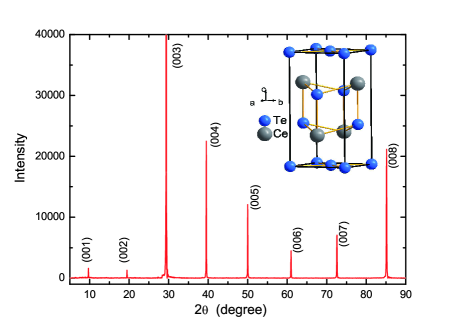
Figure 1 displays the X-ray diffraction pattern of CeTe2-x single crystals at room temperature. The (0 0 ) diffraction peaks indicate a good c-axis characteristic. The obtained c-axis lattice parameter is c=9.11, which agrees well with the previous result.xrd The energy dispersive X-ray spectroscopy (EDX) analysis equipped with the scanning electron microscope (SEM) indicates that both the La- and Ce-based compounds have average compositions of R:Te1:1.95 (R=La, Ce). The Se-doped crystal has an average composition of CeTe1.79Se0.16. Obviously, Te deficiencies are present in the crystals although the self-flux method was reported to be effective on reducing the Te vacancies.fisherRTe2 As we shall elaborate in this work, those Te vacancies greatly affect the optical properties of RTe2 systems.
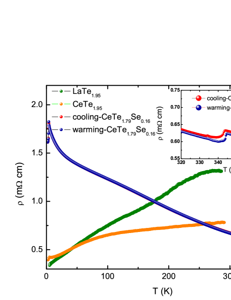
The temperature dependence of the in-plane (ac-plane) dc conductivity was measured by a standard four-probe method in a quantum design physical properties measurement system (PPMS) and plotted in Fig. 2. Platinum wires were fixed on the sample using highly conducting silver adhesive in the glove-box to avoid deterioration. The resistivity of both CeTe1.95 and LaTe1.95 shows metallic behavior with relatively high absolute values at base temperature in comparison with RTe3. In an earlier report by by Shin et al. fisherRTe2 , the resistivity of LaTe1.95 shows an upturn at low temperature. The different behaviors could be attributed to slightly different sample quality. Due to Te deficiencies, values change between crystals Resist ; fisherRTe2 . In addition, CeTe1.95 compound shows a sharp feature at about 5K, which is related to the anti-ferromagnetic ordering of spins from the localized 4f electrons of Ce. On the other hand, the resistivity behavior is rather different when Te was partially substituted by Se. The resistivity of CeTe1.95-xSex (x=0.16) increases modestly with decreasing temperature. An anomaly is surprisingly seen near 345 K both in cooling and warming processes. We performed transmission electron microscopy (TEM) measurement on this sample and found that the superlattice diffraction spots disappear at temperatures above 345 K. Combined with the results from optical study below, we believe that it could be ascribed to CDW phase transition.
The optical reflectivity measurement was carried out on Bruker IFS 113v and 80v/s spectrometers in a frequency range from 40 to 25000 cm-1. An in situ gold and aluminium overcoating technique was used to get the reflectivity R(). Kramers-Kronig transformation of R() is employed to get the real part of the conductivity spectra . A Hagen-Rubens relation was used for the low frequency extrapolation. A constant value of high frequency extrapolation was used up to 100000 cm-1 , above which an relation was employed.
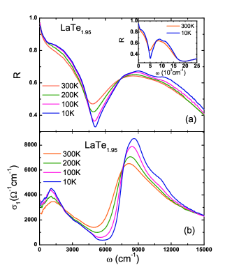
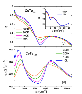
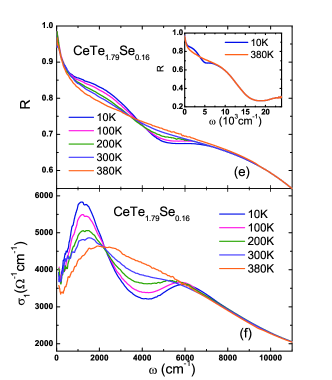
Figure 3 show the optical reflectance R() and real part of conductivity of LaTe1.95, CeTe1.95-xSex (x=0 and 0.16), respectively. The insets of upper panels show R() in the expanded rang up to 25000 cm-1 . The R() of the those compounds have high values at low frequency and decreases rapidly with increasing frequency, forming plasma edges near 18000 cm-1 . The experimental results demonstrate that the materials are metallic even in the deep CDW state, consistent with the dc resistivity measurements.
Two significant features exist in the optical spectra of those samples. The first one is the very strong dip structure in R() in the near infrared region 5000 cm-1 , which becomes more pronounced upon cooling. This leads to a remarkable peak structure in the conductivity spectra at higher energy scale. For the three samples, the conductivity peak is the most prominent for the LaTe1.95 crystal. It locates near 8000 cm-1 at 300 K, and shifts to further higher energy scale 8500 cm-1 as the temperature decreases to 10 K. For the pure and Se-doped CeTe1.95 samples, the peak feature appears at lower energy scales and also becomes less pronounced. The spectra provide optical evidence for the presence of an energy gap, which could be ascribed to the CDW order. Because of the "type-I coherent factor" for density wave order which gives rise to a characteristic peak structure just above the energy gap in optical conductivity, the peak position in could be identified as the energy scale of CDW gap.HuSDW ; electrondynamic The measurement results are in agreement with earlier reports.Lavagnini ; optCeTe2 In ARPES measurements, the inner FSs centered at point were found to be almost fully gapped with Eg=600 meV (roughly 4800 cm-1 ) for LaTe1.95 fisherRTe2 . Since the ARPES measurement probes the gap relative to the Fermi level, while the optical measurement detects the excitation from occupied to unoccupied states, the gap value by optics should double the gap size probed by ARPES. Roughly, the gap values are consistent with earlier ARPES experiments fisherRTe2 . For the Se-doped CeTe1.95-xSex (x=0.16), since a resistivity jump is observed near 345 K, the CDW order is believed to be formed only below this temperature. Indeed, we found an absence of this gap feature in reflectance and conductivity spectra at measurement temperature 380 K.
The second very strong structure is the presence of another prominent peak in conductivity spectra at much lower energy scale, between 800-1500 cm-1 for LaTe1.95 and CeTe1.95-xSex (x=0, 0.16). This peak structure was also observed in earlier optical measurements and was assigned to an energy gap as welloptCeTe2 . Indeed, ARPES measurements revealed energy gap features roughly at the half of above values. Nevertheless, we noticed that the peak positions in moves slightly towards the lower energy as temperature decreases for those compounds. Such temperature dependent shift is opposite to the expectation of CDW energy gap formation. On this account, the low-energy peak structure could not be ascribed to the formation of a small CDW gap. This conclusion is further strengthened by the measurement on Se-doped CeTe1.95-xSex (x=0.16). For this sample, the CDW phase transition is already suppressed to 345 K. In accordance with this suppression, the energy gap feature near 6000 cm-1 is not visible in our optical measurement at 380 K. However, the low-energy peak feature is still present at all measurement temperatures. If the low-energy peak feature is developed from CDW order, it should be more easily suppressed by the Se doping. Considering the fact that the Te deficiencies are always present in the RTe2-x samples and the conduction electrons are from the 5p electrons of square Te layers, we expect that the disorder-driven electron localization effect is the dominant contribution to the formation of the low-energy peak structure in . It remains to be investigated whether or not the electron localization effect, which leads to the peak structure in , could results in a gap-like feature in ARPES measurements. As we shall elaborate blow, the localization modified Drude model could reasonably reproduce the spectral feature of the experimental data.
Besides the above two very strong spectral structures, we also noticed a weak feature near 10000 cm-1 in R() for both LaTe1.95 and CeTe1.95 compounds, which is more clearly visible at low temperature and leads to a shoulder in spectra at slightly higher frequencies. Different from the notable shift of peak corresponding to CDW orders, the shoulder positions show little change at varied temperatures. It is likely that this feature comes from the inter-band transitions.
III Analysis from the localization modified Drude model
Sample LaTe1.95(10K) 21 1.5 1.3 8.5 2 27 10 5 30 23 40 60 LaTe1.95(300K) 21.3 2 1.07 8 2.5 24.7 10 5.3 29 23 40 60 CeTe1.95(10K) 26 1.3 1.18 6.8 2.4 22 8.8 5.6 29 22 40 65 CeTe1.95(300K) 27 2 1.12 6.2 3.4 21 8.3 5.7 28 22 40 65 CeTe1.79Se0.16(10K) 23 1.6 0.9 6 3.2 14 9 14.7 36 - - - CeTe1.79Se0.16(380K) 34 4 1.14 - - - 9 19 32 - - -
Let us now analyze the evolution of the itinerant carriers and the CDW gap excitations in a quantitative way. As stated above, we try to use the localization modified Drude (LMD) model, instead of a simple Drude term, to analyze the low frequency conductivity spectra, since the former is more appropriate in a carriers-localization system.GLi ; Mott ; handbook The high frequency interband transitions and energy gap excitations could be described by the Lorentz components. Within the LMD and Lorentz approach, the dielectric function would consist of two parts:
| (1) |
and
| (2) |
Here, the first term in expression (1) is the LMD component, the second term is the Lorents components. is the dielectric constant at high energy, the plasma frequency, the Fermi wave vector, the mean free path and C a universal constant(). The model was found to reproduce the conductivity spectra fairly well. As examples, we show in Fig. 4 the experimental data together with the fitting curves for CeTe1.95-xSex (x=0 and 0.16) samples at 10 K, respectively. In Table 1 we list the fitting parameters for the three different samples at 300 (or 380) and 10 K, respectively. The disorder parameter () is in general greater than 1, which is in the metallic side of the metal-insulator transition in terms of Ioffe-Regel criterion. The model yields consistent values with the dc conductivity at the zero frequency limit where it takes the form for the metallic conduction,
| (3) |
This expression could account for the reduction of conductivity due to localization effect when .Homes Apparently, the LMD model is more suitable in describing the carrier response in the infrared region as it can account for the disorder effect presented in the samples. Nevertheless, it should be remarked that the () parameter becomes slightly smaller than 1 for CeTe1.95-xSex (x=0.16) sample at low temperature, indicating further enhanced localization effect. This effect could be naturally attributed to the random substitutions of Te sites by Se in the conducting Te layers, which drives the sample into the non-metallic side of the Ioffe-Regel criterion. The result is consistent with the semiconducting dc resistivity behavior. In this circumstance, the LMD model is no longer valid for this sample.
The above analysis indicates that the free carrier response can be described by the LMD component. We found that of both LaTe1.95 and CeTe1.95 decreases very slightly from room temperature to 10K. On the other hand, the scattering rate ( = 1/) decreases even faster. However, for CeTe1.95-xSex (x=0.16), the plasma frequency = 33600 cm-1 at 380 K reduces to 23000 cm-1 at 10 K. The square of plasma frequency is proportional to the effective carrier density n/m∗ (where m∗ is the effective carrier mass). This result could be interpreted as the formation of the partial CDW gap which removes those electrons near that experience stronger scattering, leading to a reduction of both conducting carrier density and the scattering rate due to the reduction of scattering channels.
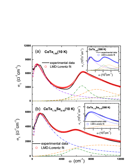
Our study indicates that the Te-vacancies or disorder effect play the key role in the low-energy charge excitations of rare-earth ditellurides RTe2-x. This is different from the extensively investigated rare-earth tri-telluride RTe3 where Te vacancies were usually not detected. We would also like to remark that the disorder effect could also dramatically affect the CDW phase transitions.
As already discussed above, the CDW energy gap could be identified from the peak position of the first Lorentz oscillation in the conductivity spectrum. At the lowest temperature, the Lorentz peak locates near 8500 cm-1 for LaTe1.95 and 6800 cm-1 for CeTe1.95, respectively. Those values are larger than the corresponding values of rare-earth tri-tellurides. Such large energy gap values would imply that the compounds are already deeply in the CDW state even at room temperature. With Se doping, CDW energy gap is reduced and the CDW order is suppressed. However, the reduction of the energy gap is small. In comparison with the undoped sample CeTe1.95, the Lorentz peak, which locates at 6000 cm-1 , is shifted by only 800 cm-1 for CeTe1.79Se0.16 sample. Even if we assume that the ratio of the 2, a number higher than BCS value but still often seen in strongly coupling materials HuSDW , we expect that the CDW transition temperature would be still higher than 1000 K. In reality, the CDW transition temperature appears at 345 K. To our knowledge, the CDW transition temperature close to room temperature in the RTe2 system has never been observed before. Our study suggests that, in the heavily disordered system, the ratio of the CDW energy gap over the transition temperature does not follow the value as normally expected from the BCS mean-field theory for density wave instability. Compared with the undoped samples, the peak structure becomes much weaker. Our observations seem to indicate that the disorder or localization effect arising from Te vacancies or Se substitutions affects the the CDW transition temperature more radically than the energy gap. We also emphasize that our results are strongly against the conclusions drawn by Garcia et al. based on ARPES study that CDW gap size decreases dramatically as the number of the Te layers reduces from two (RTe3) to one (RTe2) and the ReTe2 would be examples of semiconducting quasi-2D CDW material due to the gapping of the entire Fermi surfaces.
IV CONCLUSIONS
To conclude, we have performed an optical study on the single-crystals of LaTe1.95, CeTe1.95 and CeTe1.79Se0.16, belonging to the layered quasi-two-dimensional charge density wave systems. Our measurement revealed clearly the formation of partial energy gaps at rather high energy levels: 2 8500 cm-1 (1.06 eV) for LaTe1.95, and 6800 cm-1 (0.84 eV) for CeTe1.95. A small fraction of Se substitutions for Te dramatically weaken the CDW order and suppress the phase transition temperature. As a result, the CDW phase transition was observed, for the first time, close to room temperature in the rare-earth ditelluride system. Our study also revealed that the low energy excitations of the compounds are dominantly contributed by the disorder effects due to the presence of Te vacancies in conducting Te layers. The localization modified Drude model can account for the low-frequency charge response fairly well. The spectral features are distinctly different from a semiconducting CDW state with fully gapped Fermi surfaces.
ACKNOWLEDGMENTS
This work was supported by the National Science Foundation of China (10834013, 11074291), and the 973 project of the Ministry of Science and Technology of China (2011CB921701, 2012CB821403).
References
- (1) G. Grüner, Density Waves in Solids (Addison-Wesley, Reading, MA, 1994).
- (2) E. DiMasi, B. Foran, M. C. Aronson, and S. Lee, Chem. Mater. 6, 1867 (1994).
- (3) V. Brouet, W. L. Yang, X. J. Zhou, Z. Hussain, N. Ru, K.Y. Shin, I. R. Fisher, and Z. X. Shen, Phys. Rev. Lett. 93, 126405 (2004).
- (4) N. Ru and I. R. Fisher, Phys. Rev. B 73, 033101 (2006).
- (5) E. DiMasi, M. C. Aronson, J. F. Mansfield, B. Foran, and S. Lee, Phys. Rev. B 52, 14516 (1995).
- (6) Kikichi, J. Phys. Soc. Jpn. 67, 1308 (1998).
- (7) J. H. Shim, J.-S. Kang, and B. I. Min, Phys. Rev. Lett. 93, 156406 (2004).
- (8) J. Laverock, S. B. Dugdale, Zs. Major, M. A. Alam, N. Ru, I. R. Fisher, G. Santi, and E. Bruno, Phys. Rev. B 71, 085114 (2005).
- (9) K. Y. Shin, V. Brouet, N. Ru, Z. X. Shen and I. R. Fisher, Phys. Rev. B 72, 085132 (2005).
- (10) E. DiMasi, B. Foran,M. C. Aronson, S. Lee, Phys. Rev. B 54, 13587 (1996).
- (11) M. H. Jung, A. Alsmadi, H. C. Kim, Yunkyu Bang, K. H. Ahn, K. Umeo, A. H. Lacerda, H. Nakotte, H. C. Ri, and T. Takabatake, 67, 212504 (2003).
- (12) B. F. Hu, P. Zheng, R. H. Yuan, T. Dong, B. Cheng, Z. G. Chen, and N. L. Wang, Phys. Rev. B 83, 155113 (2011).
- (13) B. F. Hu, B. Cheng, R. H. Yuan, T. Dong, A. F. Fang, W. T. Guo, Z. G. Chen, P. Zheng, Y. G. Shi, and N. L. Wang, Phys. Rev. B 84, 155132 (2011).
- (14) D. R. Garcia, G.-H. Gweon, S. Y. Zhou, J. Graf, C. M. Jozwiak, M. H. Jung, Y. S. Kwon, and A. Lanzara, Phys. Rev. Lett. 98, 166403 (2007).
- (15) W. B. Pearson, Zeitschrift für Kristallographie171, 23 (1985).
- (16) Y. S. Kwon and B. H. Min, Physica B 281 C282, 120 (2000).
- (17) W. Z. Hu, J. Dong, G. Li, Z. Li, P. Zheng, G. F. Chen, J. L. Luo, and N. L. Wang, Phys. Rev. Lett. 101, 257005 (2008).
- (18) M. Dressel, and G. Grüner, Electrodynamics of Solids (Cambridge, Reading, 2002).
- (19) M. Lavagnini, A. Sacchetti, L. Degiorgi, K. Y. Shin, and I. R. Fisher, Phys. Rev. B 75, 205113 (2007).
- (20) K. E. Lee, C. I. Lee, H. J. Oh, M. A. Jung, B. H. Min, H. J. Im, T. Iizuka, Y. S. Lee, S. Kimura, and Y. S. Kwon, Phys. Rev. B 78, 134408 (2008).
- (21) G. Li, P. Zheng, N. L. Wang, Y. Z. Long, Z. J. Chen, J. C. Li and M. X. Wan, J. Phys.: Condens. Matter 16 6195 (2004).
- (22) N. F. Mott, Metal-Insulator Transitions (Taylor & Francis, London, 1990).
- (23) R. Menon, C. O. Yoon, D. Moses, and A. J. Heeger, 1998 Handbook of Conducting Polymers 2nd edi, vol 2 (New York: Dekker).
- (24) G. Tzamalis, N. A. Zaidi, C. C. Homes, and A. P. Monkman, Phys. Rev. B 66, 085202 (2002).